Embed Size (px)
Citation preview
Large Scale Growth and Characterization ofAtomic Hexagonal Boron Nitride LayersLi Song,† Lijie Ci,† Hao Lu,† Pavel B. Sorokin,† Chuanhong Jin,‡ Jie Ni,†Alexander G. Kvashnin,§ Dmitry G. Kvashnin,§ Jun Lou,† Boris, I. Yakobson,† andPulickel M. Ajayan*,†
†Department of Mechanical Engineering & Materials Science, Rice University, Houston, Texas 77005,‡Nanotube Research Center, National Institute of Advanced Industrial Science and Technology (AIST), Tsukuba305-8565, Japan, and §Siberian Federal University, 79 Svobodny av., Krasnoyarsk, 660041, Russia
ABSTRACT Hexagonal boron nitride (h-BN), a layered material similar to graphite, is a promising dielectric. Monolayer h-BN, so-called “white graphene”, has been isolated from bulk BN and could be useful as a complementary two-dimensional dielectric substratefor graphene electronics. Here we report the large area synthesis of h-BN films consisting of two to five atomic layers, using chemicalvapor deposition. These atomic films show a large optical energy band gap of 5.5 eV and are highly transparent over a broad wavelengthrange. The mechanical properties of the h-BN films, measured by nanoindentation, show 2D elastic modulus in the range of 200-500N/m, which is corroborated by corresponding theoretical calculations.
KEYWORDS Boron nitride, electrical microscopy, optical and mechanical properties, computation
Boron nitride (BN) is a wide band gap III-V compoundwith remarkable physical properties and chemicalstability. Hexagonal BN is comprised of alternating
boron and nitrogen atoms in a honeycomb arrangement,consisting of sp2-bonded two-dimensional (2D) layers.1-5
Within each layer of hexagonal BN, boron and nitrogenatoms are bound by strong covalent bonds, whereas thelayers are held together by weak van der Waals forces, asin graphite. Therefore, h-BN films could be peeled off frombulk BN crystal by micromechanical cleavage4-6 and usedas a dielectric layer.6,7 Few-layer hexagonal BN has also beenmade by ultrasonication8 and high-energy electron beamirradiation of BN particles.9 The chemical decompositionreactions of various precursors have been used to demon-strate the growth of single layer BN domains over smallareas.10-13 However, methods for preparing good qualityh-BN layers over large areas would bring new opportunitiesto exploit its properties and potential applications, especiallyas interesting two-dimensional dielectric material in graphene-based electronics. Here we show uniform and continuoush-BN films on a large area have been successfully synthe-sized using a thermal catalytic chemical vapor deposition(CVD) method. These as-grown films consisting of two to fivelayers are highly transparent with a large band gap and poseunique mechanical properties.
The synthesis of h-BN films was carried out in a split tubefurnace with a fused quartz processing tube (50 mm outsidediameter). A copper foil with 25 µm thickness was used as
substrate, similar to previous reports.14-16 For the growth,the Cu foil was quick washed by dilication nitric acid anddeionized water. Then it was placed in the center of afurnace, annealed at 600 °C for 20 min in Ar/H2 (15 vol %H2, 85 vol % argon) flow with 500 sccm. As followed, thefurnace was gradually heated up to 1000 °C in 40 min.Ammonia borane (NH3-BH3) was sublimated at 120-130°C by using a heating belt and then carried into the reactionregion by Ar/H2 gas glow. During the growth process, Ar/H2
flow was kept as 200 sccm. The typical growth time is30-60 min. After growth, the furnace was cooled down toroom temperature quickly. After growth, the films werecoated with poly(methyl methacrylate) and transferred toother substrates for further characterization as reportedpreviously in graphene transfers.16,17 For characterization,JEOL-2100 field emission HRTEM was performed for high-resolution transmission electron microscopy (HRTEM), se-lected area electron diffraction (SAED), electron energy lossspectroscopy (EELS) measurements, and elemental mapping(Gatan GIF). JEOL-2010F, equipped with a postspecimenaberration corrector (CEOS), was carried out to obtain theatomic image. X-ray photoelecton spectroscopy (XPS) (PHIQuantera XPS) was performed using monochromatic alu-minum KR X-rays, and the MultiPak software was used forXPS data analyses. Raman spectroscopy (Renishaw inVia)was performed at 514.5 nm laser excitation. Electricalmeasurement was performed in a probe station with a highvacuum chamber. Optical absorption measurement(SHIMADZU UV-3600) was performed on h-BN films thatwere transferred onto optical quartz plates. For the mechan-ical tests, the as-grown h-BN film was transferred on a siliconwafer with around 1 µm well patterns. Atomic force micros-
* To whom correspondence should be addressed: tel, 1-713-3485904; fax, 1-713-3485423; e-mail, [email protected] for review: 06/23/2010Published on Web: 00/00/0000
pubs.acs.org/NanoLett
© XXXX American Chemical Society A DOI: 10.1021/nl1022139 | Nano Lett. XXXX, xxx, 000–000
PAGE EST: 6.7
1
2
3
4
5
6
7
8
9
10
11
12
13
14
15
16
17
18
19
20
21
22
23
24
25
26
27
28
29
30
31
32
33
34
35
36
37
38
39
40
41
42
43
44
45
46
47
48
49
50
51
52
53
54
55
56
57
58
59
60
61
62
63
64
65
66
67
68
69
70
71
72
73
74
75
ohio2/ynl-ynl/ynl-ynl/ynl99910/ynl5066d10z xppws 23:ver.3 7/20/10 13:20 Msc: TEID: rlt00 BATID: 00000

copy (Agilent PicoScan 5500) was used to perform thefollowing indention measurements.
Figure 1a is a photograph of as-grown h-BN film trans-ferred onto a silicon substrate, showing that the grown filmshave continuous large areas up to several square centime-ters. Panels b and c of Figure 1 show typical scanningelectron microscopy (SEM) and atomic force microscopy(AFM) images of the film. Both optical imaging and electronmicroscopy images indicate that the film is quite uniformand continuous except for some wrinkles, which may beintroduced by the transfer process and the roughness or gainboundaries present on the Cu surface.14,17 Figure 1d showsthe line-scan profile of films, indicating the as-grown filmswith thickness of about 1.3 nm.
HRTEM was performed to characterize the microstructureof these thin films. Our HRTEM observations found that theh-BN films mainly consist of two layers, as shown in Figure2a. Some of the films were composed of three to five layers(Figure 2, panels b and c). To further evaluate the crystallinityof the films, SAED was carried out on the films. The SEADof the region in Figure 2a is shown as the insert image,clearly revealing the distinctive hexagonal structure of h-BNfilms.18 We mapped the elemental distribution of B and Nin a selected area of the films by using energy-filteredtechniques (see section 1 in Supporting Information). It isfound that B and N are uniformly distributed over the entirearea of the films. We performed atomic HRTEM character-
ization by using a low voltage aberration-corrected electronmicroscopy in order to investigate the atomic structure ofthe h-BN films. Figure 2d shows a typical atomic HRTEMimage, in which the resolved features correspond to thehexagonal lattice having consistent lattice spacing with bulkh-BN.19,20 The fast Fourier transform (FFT) analysis in Figure2e reveals five sets of hexagonal spots, which indicates thatthe covered region of the Figure 2d has multiple layers. UsingEELS, we qualitatively performed elemental analysis on thefilms to determine their chemical composition and structure.Figure 2f shows an EELS spectrum with two visible edgesstarting at around 180 and 390 eV, corresponding to thecharacteristic K-shell ionization edges of B and N, respecti-vely.19,21 The two bands corresponding to each element canbe well resolved and show a first peak corresponding to the1s-π* antibonding orbit. This type of EELS edge structureproves that B and N are sp2 hybridized21,22 and indicates thatthe atomic films grown on Cu possess a hexagonal structureconsisting of B and N, which is consistent with HRTEMobservation.
The XPS spectra of as-grown h-BN films for the B and Nedges are presented in panels a and b of Figure 3, respec-tively. It is previously reported that boron nitride bulk withhexagonal phase presents the B 1s core level at 190.1eV.23,24 We find that all our samples present a B 1s-core levelat 189.9 eV (marked in Figure 3a), which is very close to thatin h-BN bulk phase. The N 1s peak is located at 397.6 eV
FIGURE 1. Topography of ultrathin hexagonal BN films. (a) Photograph of a large h-BN film on a silicon substrate. Scale bar is 1 cm. (b), SEMimage shows a h-BN film (scale bar 10 µm). (c, d) AFM image and line-scan profile indicate that h-BN film has uniform thickness of a 1 nm.Scale bar is 2 µm.
ohio2/ynl-ynl/ynl-ynl/ynl99910/ynl5066d10z xppws 23:ver.3 7/20/10 13:20 Msc: TEID: rlt00 BATID: 00000
© XXXX American Chemical Society B DOI: 10.1021/nl1022139 | Nano Lett. XXXX, xxx, 000-–000
76
77
78
79
80
81
82
83
84
85
86
87
88
89
90
91
92
93
94
95
96
97
98
99
100
101
102
103
104
105
106
107
108
109
110
111
112
113
114
115
116
117
118
119
120
121
122
123
124
125
126
127
128
129
F1
F2
F3

(marked in Figure 3b), similarly to the reported position ofthe N1s spectrum (398.1 eV) of h-BN.23,24 Both the B 1s andthe N 1s spectra indicate that the configuration for B and Natoms is the B-N bond, implying that the hexagonal phaseexists in our BN films. Figure 3c shows typical Ramanspectra taken from the h-BN thin film (top curve) and a bulkh-BN (bottom curve). At the lower frequency region, thedominant peak near 1370 cm-1 that shows up intensely forboth the film and the bulk samples is attributed to the B-Nvibrational mode (E2g) within h-BN layers.25 This Ramanspectrum further confirms the successful growth of BN filmwith a hexagonal structure. Figure 3d shows that the E2g
mode of h-BN film shifts to higher frequency compared withthat for the bulk BN. The peak shift is about 2.5 cm-1, and
the fwhm decreases from 15.5 cm-1 in bulk BN to 11.7 cm-1
in the thin film. In general, a Raman peak frequency wouldshift to higher and lower frequency under compressive andtensile stress, respectively.26 We speculate that the Ramanpeak frequency of the E2g mode shifts to higher frequencydue to an increase of stress in the h-BN films, which may begenerated by the substrate interaction and the intrinsicsurface wrinkles. At higher frequency region, the intensityof second mode for bulk BN gets suppressed due to a strongphotoluminescence background, which is shown by a broadpeak at 2765 cm-1. The second-order Raman band of h-BNfilm is fitted by two peaks located at 2270 and 2631 cm-1,as shown in the insert of Figure 3c.27,28
FIGURE 2. Microstructure of atomic layers hexagonal BN. (a) HRTEM images of the film edges indicate that the h-BN are two atomic layersthick. Some of as-grown films are three to five layers (b, c). The scale bar is 5 nm. The insert of (a) is the corresponding SEAD of the regions,which shows the hexagonal structure of h-BN film. (d) A typical atomic image of a h-BN films. The scale bars is 2 nm. (e) The FFT pattern ofa region of panel d, which indicates a five-layer stacked region. (f) EELS spectrum of a h-BN film. The C signal corresponds to small amountsof amorphous carbon which could have come from contamination on TEM grids or contamination during transfer of the BN films.
ohio2/ynl-ynl/ynl-ynl/ynl99910/ynl5066d10z xppws 23:ver.3 7/20/10 13:20 Msc: TEID: rlt00 BATID: 00000
© XXXX American Chemical Society C DOI: 10.1021/nl1022139 | Nano Lett. XXXX, xxx, 000-–000
130
131
132
133
134
135
136
137
138
139
140
141
142
143
144
145
146
147
148
149
150
151
152
153
154
155
156

Previous investigations have shown that bulk hexago-nal BN is a wide gap material. Here, we performedelectrical measurements on h-BN films devices, fabricatedby standard lithography technique (see section 2 in Sup-porting Information). We found that the h-BN films arevery good insulators. The UV-visible absorption spectrum
was carried out for investigating the optical energy gapof the h-BN film based on its optically induced transition.For this study, we first transferred large h-BN film ontoan optical quartz plate, and the quartz background wassubtracted using a blank quartz plate as the referencesubstrate. The following Tauc’s equation was used todetermine the optical band gap Eg
29
where ε is the optical absorbance and ω ) 2π/λ is theangular frequency of the incident radiation (λ is thewavelength). As Figure 3e shows, the nanometer thickh-BN film is highly transparent and can transmit over 99%of the light with wavelengths in the range of 250-900 nm.The absorption spectrum displays one sharp absorptionpeak at 203 nm. On the basis of Tauc’s formulation, it isspeculated that the plot of ε1/2/λ versus 1/λ should be astraight line at the absorption range. Therefore, theintersection point with the x axis is 1/λg (λg is defined asthe gap wavelength). The optical band gap can be calcu-lated based on Eg ) hc/λg. The insert plot of Figure 3eshows ε1/2/λ versus 1/λ curve acquired from the thin h-BNfilm. The calculated gap wavelength λg is about 223 nm,which corresponds to an optical band gap of 5.56 eV.Previous theoretical calculations of band structures for asingle layer of h-BN anticipated that equivalent bands didnot cross each other and a 6 eV band gap was the result.30
Considering two to five layers in our h-BN films, themeasured gap is smaller than the theoretical gap value ofa single layer due to the layer-layer interaction increasesthe dispersion of the electronic bands and tends to reducethe gap,30 but it is larger than that of bulk h-BN(5.2-5.4 eV).30,31
Theoretical calculations have indicated that BN layerscan be extremely strong.32 To investigate mechanicalproperties of the h-BN films, circular wells with diameteraround 1 µm were patterned onto a silicon substrate bye-beam lithography and reactive ion etching (RIE) tech-niques. The h-BN films were then transferred onto theprepatterned substrates. Figure 4a shows an ultrathin filmdeposited over many circular wells to form a series offreestanding membranes. Noncontact mode AFM test wasfirst used to obtain the thickness and find the center ofthe suspended near circular membranes. It is found thatthe h-BN films were stretched tautly across the wellopenings with about 20-50 nm sag due to the van derWaals attraction from the substrate and surface tensionduring drying process (Figure S3b in Supporting Informa-tion). The mechanical properties of the h-BN films wereprobed by indenting the center of each freestandingmembrane with a diamond tip, as illustrated in Figure 4b.The detail indention test can be found in section 3 ofSupporting Information. The elastic response of a 2D film
FIGURE 3. Spectra of hexagonal BN films. (a, b) XPS spectrum of Band N 1s core level, respectively. The spectral data (µ) are fitting byGaussian curves (red solid). (c) Raman spectrum of a h-BN film andbulk h-BN recorded at room temperature, exited by 514.5 nm laser.The inset shows the peak at high frequency. (d) Their main Ramanpeak near 1370 cm-1. The Lorenz curves (red solid) were used hereto fit the peaks. (e) Ultraviolet-visible absorption spectra of h-BNfilms taken at room temperature. The inset shows the correspondingplot of ε1/2/λ versus 1/λ.
ω2ε ) (hω - Eg)2 (1)
ohio2/ynl-ynl/ynl-ynl/ynl99910/ynl5066d10z xppws 23:ver.3 7/20/10 13:20 Msc: TEID: rlt00 BATID: 00000
© XXXX American Chemical Society D DOI: 10.1021/nl1022139 | Nano Lett. XXXX, xxx, 000-–000
157
158
159
160
161
162
163
164
165
166
167
168
169
170
171
172
173
174
175
176
177
178
179
180
181
182
183
184
185
186
187
188
189
190
191
192
193
194
195
196
197
198
199
200
201
202
203
204
205
206
207
208
209
210
211
212
213
F4
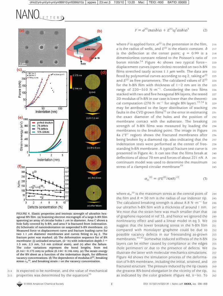
is expected to be nonlinear, and the value of mechanicalproperties was determined by the equations33
where F is applied force, σ2D is the pretension in the film,a is the radius of wells, and E2D is the elastic constant. δis the deflection at the center point; q ) 0.99 is adimensionless constant related to the Poisson’s ratio ofboron nitride.34 Figure 4c shows two typical force-displacement curves (open circles) recorded on two h-BNfilms stretched tautly across 1.1 µm wells. The data arefitted by polynomial curves according to eq 2, taking σ2D
and E2D as free parameters. The calculated values of E2D
for the h-BN film with thickness of 1-2 nm are in therange of 220-510 N·m-1. Considering the two filmsstacked with two and five hexagonal BN layers, the tested2D modulus of h-BN in our case is lower than the theoreti-cal computation (270 N·m-1 for single BN layer).33,34 Itmay be attributed to the layer distribution of stackingfaults in the CVD grown films35 or the error in estimatingthe exact diameter of the holes and the position ofmembrane contact with the substrate. The breakingstrength of h-BN films was measured by loading themembranes to the breaking point. The image in Figure4a (“F” region) shows the fractured membranes afterbeing broken by a diamond tip, also indicating that theindentation tests were performed at the center of free-standing h-BN membrane. A typical fracture test curve ispresented in Figure 4c. It can see that the films break atdeflections of about 70 nm and forces of about 221 nN. Acontinuum model was used to determine the maximumstress of a clamped circular membrane33
where σm2D is the maximum stress at the central point of
the film and R ) 50 nm is the radius of our indenter tip.The calculated breaking strength is about 8.8 N·m-1 forour ultrathin h-BN film with a thickness of around 1 nm.We note that the strain here was much smaller than thatof graphene reported in ref 33, and hence we ignored thenonlinearity effect and used a linear model in eq 3. Wesuggest that the lower breaking stress in the h-BN filmcompared with monolayer graphene could be due topossible vacancy defects in our freestanding as-grownmembranes.33,35 Somewhat reduced stiffness of the h-BNlayers can be either caused by compliance at the edges(hole perimeter) or due to the presence of defects. Weillustrate the latter with molecular mechanics simulations.Figure 4d shows the simulation process of the deforma-tion of h-BN membrane, including the initial, strained, andfractured structure. The pressure induced by the tip causesthe greatest BN-bond elongation in the vicinity of the tip,as indicated by the color gradient (Figure 4d, ii-iv). To
FIGURE 4. Elastic properties and intrinsic strength of ultrathin hex-agonal BN film. (a) Scanning electron micrograph of a large h-BN filmspanning an array of circular holes 1 µm in diameter. Area C shows ahole fully covered by h-BN, and area F is fractured from indentation.(b) Schematic of nanoindentation on suspended h-BN membrane. (c)Measured force vs displacement curve and fracture loading curve fortwo 1.1 µm diameter membranes and curves fitting to eq 2. Thefracture point was marked. (d) The deformation sequence for of BNmembrane: (i) unloaded structure, (ii-iv) with indentation depth δ )1.5 nm, 2.5 nm, 3.0 nm (critical stain), and (v) after the failure.The color variations represent the bond lengths, from red(0.161-0.175 nm) to yellow (0.144-0.146 nm). (e) The strain energyof the BN sheet as a function of the indentation depth, for differentvacancy concentrations. (f) The dependence of modulus E2D, breakingstress σm
2D, and breaking strain ε on the vacancy concentration.
F ) σ2D(πa)(δ/a) + E2D(q3a)(δ/a)3 (2)
σm2D ) (FE2D/4πR)1/2 (3)
ohio2/ynl-ynl/ynl-ynl/ynl99910/ynl5066d10z xppws 23:ver.3 7/20/10 13:20 Msc: TEID: rlt00 BATID: 00000
© XXXX American Chemical Society E DOI: 10.1021/nl1022139 | Nano Lett. XXXX, xxx, 000-–000
214
215
216
217
218
219
220
221
222
223
224
225
226
227
228
229
230
231
232
233
234
235
236
237
238
239
240
241
242
243
244
245
246
247
248
249
250
251
252
253
254
255
256
257
258
259
260
261
262

emulate the AFM tip, a hemisphere of mutually staticatoms strain the h-BN membrane with fixed edges up toits failure. At critical strain level, the film fails with a visiblepuncture in the center. The computed strain energy(Figure 4e) is then fitted to the integral of eq 2, to obtainthe coefficient E2D.
For the computation model, we chose a BN sheet ofdiameter 14.8 nm and a tip of diameter 1.63 nm. Then foran initially perfect BN sheet, we obtain E2D ) 292.1 N·m-1,in accordance with earlier ab initio results (271 N/m).34 Wesimulated the behavior of BN sheets with 1-10% vacancyconcentrations. Due to variability in defect distributions, weperformed 10 computational tests for each of the concentra-tion values and plotted the obtained data in Figure 4e. TheE2D values decrease almost linearly with defect concentra-tion, down to 115.4 ( 14.8 N/m (at 10% vacancies). Theσm
2D decreases linearly from 71.7 N/m (perfect BN) to 26.6( 1.7 N/m (10% vacancies). It is important to note that thebreaking strain e ) ⟨σm
2D⟩/⟨E2D⟩ ≈ 0.22 is nearly unaffectedby vacancies. This contrasts with the well-known stress-concentration by microcracks but is understandable foratomic-size voids. A comparison between tested mechanicalvalues and theoretical computations is listed in Table 1. Moreinformation of computeration is shown in section 4 of theSupporting Information. Here, we want to point out thatthe tested values may have been underestimated due to thenonsharp edges of the wells and the possible underestima-tion of the diameter of freestanding BN membranes. Pos-sible defect distribution in the films could also contribute tothe relatively lower values in our tip-indentation experiments.
As to the growth mechanism of hexagonal boron nitride,it has been observed that small area h-BN layers, such asBN nanomeshes and islands, could be synthesized by de-composed borazine (HBNH)3 or B-trichloroborazine (CIBNH)3ontransitionmetalsurfacesusingaCVDprocessat1000-1100K.12,36 In our synthesis, the copper substrate has a latticeconstant similar to that of the in-plane lattice constant ofh-BN (0.255 nm versus 0.25 nm). The copper substrateshows catalytic activity for the decomposition of ammoniaborane (NH3-BH3). During growth, the ammonia boranewas sublimed first and transferred to a high temperaturezone for decomposition. The decomposition of NH3-BH3
vapor at 1300 K on a copper surface supplies both boronand nitrogen onto the metallic substrate, leading to surfacediffusion of these species and a surface-mediated growth ofh-BN films, which is similar to the growth mechanism
proposedforgrapheneandBN-Chybridlayersoncopper.14,16,37
As the growth seems to occur by a surface-mediated process,the quality of copper foil plays a key role in controlling theformation of continuous layers on the substrate and thenumber of layers of h-BN formed. It is not clear however whythe growth produces mostly multiple layers of h-BN and nota single layer; with further optimization of growth param-eters, this could be achieved in the future but for applicationsinvolving the use of h-BN layers as dielectric, a few layerstructure may suffice.
In summary, we have synthesized two-dimensional atomiclayers of hexagonal BN films over large areas and transferredthem successfully to many substrates. These 2D dielectricfilms with a large optical band gap of 5.56 eV show highoptical transparency in the UV-visible range. The mechan-ical properties of the h-BN film were measured via nanoin-dentation and theoretical models and this showed thedependence of the in-plane stiffness of the films to intrinsicdefects present in the films. Our synthesis method couldpave a way for investigating the unique structure andproperties of h-BN thin films38 and exploiting its largenumber of potential applications39,40 including its use as adielectric to complement graphene devices.
Acknowledgment. P.M.A. acknowledge support fromRice University startup funds and funding support from theOffice of Naval Research (ONR) through the MURI programon graphene and the Basic Energy Sciences division of theDepartment of Energy (DOE). L.S. was supported by DOE-BES program DE-SC0001479 for the growth and character-ization. L.C. was supported by the ONR MURI program(Award No N00014-09-1-1066) for TEM characterization. C.J.acknowledges the International Balzan Foundation for fi-nancial support through Meijo University. J.N. acknowledgesthe scholarship from Chinese State Scholarship fund. H.L.and J.L. acknowledge support from NSF (ECCS-0702766) andthe Welch Foundation (C-1716). P.S. and B.Y. acknowledgesupport from a DOE grant (DE-FG02-09ER46598).
Supporting Information Available. Elemental mappingby transmission electron microscopy on the h-BN film,electrical measurement on the h-BN film, detail of theindentation measurements by atomic force microscopy, andmolecular mechanics computation of h-BN layer.This ma-terial is available free of charge via the Internet at http://pubs.acs.org.
REFERENCES AND NOTES(1) Watanabe, K.; Taniguchi, T.; Kanda, H. Direct-bandgap properties
and evidence for ultraviolet lasing of hexagonal boron nitridesingle crystal. Nat. Mater. 2004, 3, 404–409.
(2) Kubota, Y.; Watanabe, K.; Tsuda, O.; Taniguchi, T. Deep ultra-violet light-emitting hexagonal boron nitride synthesized atatmospheric pressure. Science 2007, 317, 932–934.
(3) Golberg, D.; Bando, Y.; Huang, Y.; Terao, T.; Mitome, M.; Tang,C.; Zhi, C. Boron nitride nanotubes and nanotsheets. ACS Nano2010, 4, 2979–2993.
(4) Pacile, D.; Meyer, J. C.; Girit, C. O.; Zettl, A. The two-dimensionalphase of boron nitride: few-atomic-layer sheets and suspendedmembranes. Appl. Phys. Lett. 2008, 92, 133107–1.
TABLE 1. The Comparison of Mechanical Properties of h-BNFilms with Different Thicknesses and Theoretical ComputationValues
samplethickness
(nm)possiblelayer no. E2D (N/m) σm
2D (N/m)
A 2.0 ( 0.1 ∼5 503 ( 30 15.7 ( 1.5B 1.65 ( 0.1 ∼4 431 ( 21 12.8 ( 1.3C 1.03 ( 0.1 ∼2 223 ( 16 8.8 ( 1.2theoreticalcomputation 0.33 1 292.1 71.7
ohio2/ynl-ynl/ynl-ynl/ynl99910/ynl5066d10z xppws 23:ver.3 7/20/10 13:20 Msc: TEID: rlt00 BATID: 00000
© XXXX American Chemical Society F DOI: 10.1021/nl1022139 | Nano Lett. XXXX, xxx, 000-–000
263
264
265
266
267
268
269
270
271
272
273
274
275
276
277
278
279
280
281
282
283
284
285
286
287
288
289
290
291
292
293
294
295
296
297
298
299
300
301
302
303
304
305
306
307
308
309
310
311
312
313
314
315
316
317
318
319
320
321
322
323
324
325
326
327
328
329
330
331
332
333
334
335
336
337
338
339
340
341
342
343
344
345
346
347
348
349
350
351
352
353
354355356357358359360361362363364365
T1

(5) Lee, C. G.; Li, Q.; Kalb, W.; Liu, X.; Berger, H.; Carpick, R. W.;Hone, J. Frictional characteristics of atomically thin sheets. Science2010, 328, 76–80.
(6) Dean, C. R.; Young, A. F.; Meric, I.; Lee, C.; Wang, L.; Sorgenfrei,S.; Watanabe, K.; Taniguchi, T., Kim, P.; Shepard, K. L.; Hone, J.Boron nitride substrates for high quality graphene electronics.arXiv: 1005.4917, 2010.
(7) Giovannetti, G.; Khomyakov, P.; Brocks, G.; Kelly, P.; Brink, J.V. D. Substrate-induced band gap in graphene on hexagonalboron nitride: Ab initio density functional calculations. Phys. Rev.B 2007, 76, No. 073103.
(8) Zhi, C.; Bando, Y.; Tang, C.; Kuwahara, H.; Golberg, D. Large-scale fabrication of boron nitride nanosheets and their utilizationin polymeric composites with improved thermal and mechanicalproperties. Adv. Mater. 2009, 21, 2889–2893.
(9) Mayer, J. C.; Chuvilin, A.; Algara-Siller, G.; Biskupek, J.; Kaiser,U. Selective sputtering and atomic resolution imaging of atomi-cally thin boron nitride membranes. Nano Lett. 2009, 9, 2683–2689.
(10) Nag, A.; Raidongia, K.; Hembram, K. P. S. S.; Datta, R.;Waghmare, U. V.; Rao, C. N. R. Graphene analogues of BN: novelsynthesis and properties. ACS Nano 2010, 4, 1539–1544.
(11) Nagashima, A.; Tejima, N.; Gamou, Y.; Kawai, T.; Oshima, C.Electronic structure of monolayer hexagonal boron nitride phy-sisorbed on metal surfaces. Phys. Rev. Lett. 1995, 75, 3918–3921.
(12) Corso, M.; Auwarter, W.; Muntwiler, M.; Tamai, A.; Greber, T.;Osterwalder, J. Boron nitride nanomesh. Science 2004, 303, 217–220.
(13) Auwarter, W.; Suter, H. U.; Sachdev, H.; Greber, T. Synthesis ofone monolayer of hexagonal boron nitride on Ni(111) fromB-Trichloroborazine (CIBNH)3. Chem. Mater. 2004, 16, 343–345.
(14) Li, X.; Cai, W.; An, J.; Kim, S.; Nah, J.; Yang, D.; Piner, R.;Velamakanni, A.; Jung, I.; Tutuc, E.; Banerjee, S. K.; Colombo,L.; Ruoff, R. S. Large-area synthesis of high-quality and uniformgraphene films on copper foils. Science 2009, 324, 1312–1314.
(15) Preobrajenski, A. B.; Vinogradov, A. S.; Martensson, N. Monolayerof h-BN chemisorbed on Cu(111) and Ni(111). Surf. Sci. 2005, 582,21–30.
(16) Ci, L.; Song, L.; Jin, C.; Jariwala, D.; Wu, D.; Li, Y.; Srivastava, A.;Wang, Z. F.; Storr, K.; Balicas, L.; Liu, F.; Ajayan, P. M. Atomiclayers of hybridized boron nitride and graphene domains. Nat.Mater. 2010, 9, 430–435.
(17) Li, X.; Zhu, Y.; Cai, W.; Borysiak, M.; Han, B.; Chen, D.; Piner,R. D.; Colombo, L.; Ruoff, R. S. Transfer of large-area graphenefilms for high-performance transparent conductive electrodes.Nano Lett. 2009, 9, 4359–4363.
(18) Regan, W.; Alem, N.; Aleman, B.; Geng, B.; Girit, C.; Maserati, L.;Wang, F.; Crommie, M.; Zettl, A. A direct transfer of layer-areagraphene. Appl. Phys. Lett. 2010, 96, 113102.
(19) Jin, C.; Lin, F.; Suenaga, K.; Iijima, S. Fabrication of a freestandingboron nitride single layer and its defect assignments. Phys. Rev.Lett. 2009, 102, 195505.
(20) Alem, N.; Emi, R.; Kisielowski, C.; Rossell, M. D.; Gannett, W.;Zettl, A. Atomically thin hexagonal boron nitride probe by ultra-high-resolution transmission electron microscopy. Phys. Rev. B2009, 80, 155425–1.
(21) Chopra, N. G.; Luyken, R. J.; Cherrey, K.; Crespi, V. H.; Cohen,M. L.; Louie, S. G.; Zettl, A. Boron nitride nanotubes. Science 1995,269, 966–967.
(22) Wibbelt, M.; Kohl, H.; Kohler-Redlich, Ph. Multiple-scatteringcalculations of electron-energy-loss near-edge structrues of exist-ing and predicted phases in the ternary system B-C-N. Phys. Rev.B 1999, 59, 11739–11745.
(23) Moulder, J. F.; Stickle, W. F.; Sobol, P. E.; Bombem, D. Handbookof X-ray Photoeletron spectroscopy; Chastain, J., Ed.; Perkin ElmerCo.: Eden Prairie, MN, 1992.
(24) Park, K. S.; Lee, D. Y.; Kim, K. J.; Moon, D. W. Observation of ahexagonal BN surface layer on the cubic BN film grown by dualion beam sputter deposition. Appl. Phys. Lett. 1997, 70, 315–317.
(25) Geick, R.; Perry, C. H.; Rupprecht, G. Normal modes in hexagonalboron nitride. Phys. Rev. 1966, 146, 543–547.
(26) Kuzuba, T.; Sato, Y.; Yamaoka, S.; Era, K. Raman-scattering studyof high-pressure effects on the anisotropy of force constants ofhexagonal boron nitride. Phys. Rev. B 1978, 18, 4440–4443.
(27) Wu, J.; Han, W.; Walukiewicz, W.; Ager, J. W., III; Shan, W.; Haller,E. E.; Zettl, A. Raman spectroscopy and time-resolved photolu-minescence of BN and BCN nanotubes. Nano Lett. 2004, 4, 647–650.
(28) Ferrari, A. C.; Meyer, J. C.; Scardaci, V.; Casiraghi, C.; Lazzeri, M.;Mauri, F.; Piscanec, S.; Jiang, D.; Novoselov, K. S.; Roth, S.; Geim,A. K. Raman spectrum of graphene and graphene layers. Phys.Rev. Lett. 2006, 97, 187401.
(29) Tauc, J.; Grigorovici, R.; Vancu, A. Optical properties and elec-tronic structure of amorphous germanium. Phys. Status Solidi1996, 15, 627–637.
(30) Blase, X.; Rubio, A.; Louie, S. G.; Cohen, M. L. Quasiparticle bandstructure of bulk hexagonal boron nitride and related systems.Phys. Rev. B 1995, 51, 6868–6875.
(31) Zunger, A.; Katzir, A.; Halperin, A. Optical properties of hexagonalboron nitride. Phys. Rev. B 1976, 13, 5560–5573.
(32) Hemandez, E.; Goze, C.; Bernier, P.; Rubio, A. Elastic propertiesof C and BCN composite nanotubes. Phys. Rev. Lett. 1998, 68,4502–4505.
(33) Lee, C.; Wei, X.; Kysar, W. J.; Hone, J. Measurement of the elasticproperties and intrisic strength of monolayer graphene. Science2008, 321, 385–388.
(34) Kudin, K. N.; Scuseria, G. E.; Yakobson, B. I. C2F, BN, and Cnanoshell elasticity from ab inition computations. Phys. Rev. B2001, 64, 235406.
(35) Li, C.; Bando, Y.; Zhi, C.; Huang, Y.; Golberg, D. Thickness-dependentbendingmodulusofhexagonalboronnitridenanosheets.Nanotechnology 2009, 20, 385707.
(36) Auwarter, W.; Suter, H. U.; Sachdev, H.; Greber, T. Synthesis ofone monolayer of hexagonal boron nitride on Ni(111) fromB-Trichloroborazine. Chem. Mater. 2004, 16, 343–345.
(37) Li, X.; Cai, W.; Colombo, L.; Ruoff, R. S. Evolution of graphenegrowth on Ni and Cu by carbon isotope labeling. Nano Lett. 2009,9, 4268–4272.
(38) Stephan, O.; Ajayan, P. M.; Colliex, C.; Redlich, Ph.; Lambert,J. M.; Bernier, P.; Lefin, P. Doping graphitic and carbon nanotubestructures with boron and nitrogen. Science 1994, 266, 1683–1685.
(39) Davis, R. F. III-V Nitrides for electronic and optoelectronicapplications. Proc. IEEE 1991, 79, 702–712.
(40) Engler, M.; Lesniak, C.; Ruisinger, B.; Eichler, J. Hexagonal boronnitride (hBN)-applications from metallurgy to cosmetics. Cfi/Ber.DKG 2007, 84, E49–E53.
ohio2/ynl-ynl/ynl-ynl/ynl99910/ynl5066d10z xppws 23:ver.3 7/20/10 13:20 Msc: TEID: rlt00 BATID: 00000
© XXXX American Chemical Society G DOI: 10.1021/nl1022139 | Nano Lett. XXXX, xxx, 000-–000
PAGE EST: 6.7
366367368369370371372373374375376377378379380381382383384385386387388389390391392393394395396397398399400401402403404405406407408409410411412413414415416417418419420421422423424
425426427428429430431432433434435436437438439440441442443444445446447448449450451452453454455456457458459460461462463464465466467468469470471472473474475476477478479480481482