Embed Size (px)
Citation preview
Large Area and High Efficiency Photon Counting Imaging Detectors with High Time and Spatial Resolution for Night Time Sensing and Astronomy
Oswald H. W. Siegmund, John V. Vallerga, Anton S. Tremsin, Jason B. McPhate
Space Sciences Laboratory, U.C. Berkeley Xavier Michalet, Shimon Weiss
University of California Los Angeles Henry Frisch
University of Chicago Robert Wagner, Anil Mane, Jeffrey Elam Argonne National Laboratory, Chicago Il
Gary Varner University of Hawaii
ABSTRACT
Imaging sensors using GaAs photocathodes of 18 mm active area format with microchannel plates and cross strip
readouts in sealed tubes have been developed. The GaAs photocathodes have peak quantum efficiency of ~30% from 550 nm to 850 nm and background rates of ~50 kHz at 8° C. The sensor system including our processing electronics achieves spatial resolution of ~40 µm FHWM (at gains of ~ 106), can process high event rates (5 MHz input rates), has event timing accuracy of ~360 ps and local area counting rates of up to 20 kHz (100 µm spot). We have also made significant progress on development of novel large area (20 cm) microchannel plates and their implementation into sealed tube devices. These microchannel plates have demonstrated better than 100µm spatial resolution, low background rates (0.1 events cm-2 sec-1), and very good lifetime stability to 7 C cm-2 of charge extraction. Considerable progress in development of a 20 cm format sealed tube device has also been made including the demonstration of 20 cm bialkali photocathodes with stable peak (360 nm) quantum efficiency of > 20%.
Keywords: Microchannel plate, photon counting, imaging, timing
1. INTRODUCTION
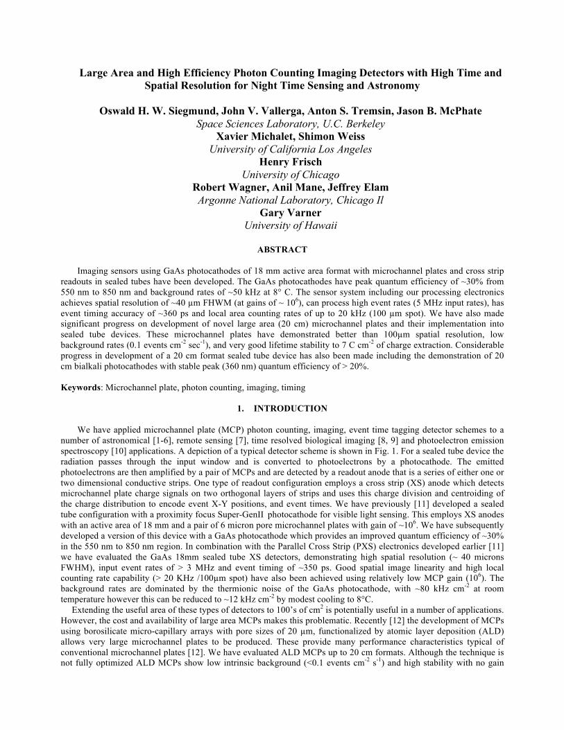
We have applied microchannel plate (MCP) photon counting, imaging, event time tagging detector schemes to a number of astronomical [1-6], remote sensing [7], time resolved biological imaging [8, 9] and photoelectron emission spectroscopy [10] applications. A depiction of a typical detector scheme is shown in Fig. 1. For a sealed tube device the radiation passes through the input window and is converted to photoelectrons by a photocathode. The emitted photoelectrons are then amplified by a pair of MCPs and are detected by a readout anode that is a series of either one or two dimensional conductive strips. One type of readout configuration employs a cross strip (XS) anode which detects microchannel plate charge signals on two orthogonal layers of strips and uses this charge division and centroiding of the charge distribution to encode event X-Y positions, and event times. We have previously [11] developed a sealed tube configuration with a proximity focus Super-GenII photocathode for visible light sensing. This employs XS anodes with an active area of 18 mm and a pair of 6 micron pore microchannel plates with gain of ~106. We have subsequently developed a version of this device with a GaAs photocathode which provides an improved quantum efficiency of ~30% in the 550 nm to 850 nm region. In combination with the Parallel Cross Strip (PXS) electronics developed earlier [11] we have evaluated the GaAs 18mm sealed tube XS detectors, demonstrating high spatial resolution (~ 40 microns FWHM), input event rates of > 3 MHz and event timing of ~350 ps. Good spatial image linearity and high local counting rate capability (> 20 KHz /100µm spot) have also been achieved using relatively low MCP gain (106). The background rates are dominated by the thermionic noise of the GaAs photocathode, with ~80 kHz cm-2 at room temperature however this can be reduced to ~12 kHz cm-2 by modest cooling to 8°C.
Extending the useful area of these types of detectors to 100’s of cm2 is potentially useful in a number of applications. However, the cost and availability of large area MCPs makes this problematic. Recently [12] the development of MCPs using borosilicate micro-capillary arrays with pore sizes of 20 µm, functionalized by atomic layer deposition (ALD) allows very large microchannel plates to be produced. These provide many performance characteristics typical of conventional microchannel plates [12]. We have evaluated ALD MCPs up to 20 cm formats. Although the technique is not fully optimized ALD MCPs show low intrinsic background (<0.1 events cm-2 s-1) and high stability with no gain
degradation over at least 7 C cm-2 of charge extraction. Initial tests in a large detectors with a cross strip or cross delay line readouts have achieved better than 100µm imaging with single photon sub-ns timing and MHz event rates. Significant progress has also been made in development of a 20 cm sealed tube detector and its associated readout electronics. In concert with this effort we have made stable, uniform 20 cm bialkali photocathodes with >20% quantum efficiency on borosilicate windows compatible with construction of the large sealed tube devices.
2. GALLIUM ARSENIDE PHOTOCATHODE CROSS STRIP SEALED TUBE DETECTOR
We have previously described our imaging MCP tube with a XS readout and Super-GenII photocathode in detail [11]. The results we present below use the same tube design, but employs a gallium arsenide (GaAs) semi-transparent photocathode fabricated by Photonis-NL, with a substantial quantum efficiency increase. We review the details of the design, and then present efficiency, dark rates, photon imaging and timing results. 2.1 Cross Strip – Microchannel Plate Detector Scheme
We have implemented the XS anode as a multi-layer metal and ceramic structure on an alumina substrate. The substrate has strip conductors on a ~0.6 mm period. The materials used to construct XS anodes in this way have low outgassing, and accommodate >800°C temperatures, making them compatible with sealed tube ultra high vacuum devices. The XS anodes are spaced ~2.5 mm behind the MCP stack and each strip signal is connected through a hermetic via to the back of the anode. A fan out (Fig. 3) outside the vacuum is implemented to accommodate a standard connector for the electronics. The MCP charge cloud is adjusted using a MCP-anode gap voltage so that charge is collected on several neighboring fingers (Fig. 1) to ensure an accurate event centroid can be determined [13]. Two MCPs provide sufficient electron gain (~ 106) for high resolution imaging with XS anodes. A GaAs photocathode was functionalized on a glass window by Photonis-NL and sealed to the tube after MCP conditioning.
Fig. 1. Schematic of a cross strip anode sensor. Photons are Fig. 2. 18mm GaAs photocathode, sealed tube detected by a photocathode deposited on a window facing sensor with a 22 mm cross strip readout anode a pair of MCPs. Emitted photo-electrons are multiplied by the and a pair of 6µm pore MCPs for single photon MCPs and collected by several strips in each axis of the anode. counting, event timing, imaging applications. 2.2 GaAs Sealed Tube Cross Strip Anode Microchannel Plate Sensors – QE and Dark Rate
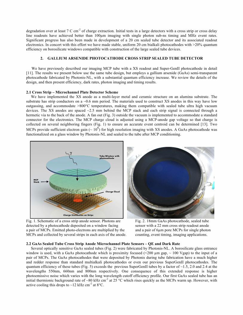
Several optically sensitive GaAs sealed tubes (Fig. 2) were fabricated by Photonis-NL. A borosilicate glass entrance window is used, with a GaAs photocathode which is proximity focused (<200 µm gap, ~ 100 Vgap) to the input of a pair of MCPs. The GaAs photocathodes that were deposited by Photonis during tube fabrication have a much higher and redder response than standard multialkali photocathodes or even our previous SuperGenII photocathodes. The quantum efficiency of these tubes (Fig. 5) exceeds the previous SuperGenII tubes by a factor of ~1.5, 2.0 and 2.4 at the wavelengths 550nm, 660nm and 800nm respectively. One consequence of this extended response is higher photoemissive noise which varies with the long wavelength cutoff efficiency profile. Our first GaAs sealed tube has an initial thermionic background rate of ~80 kHz cm-2 at 25 °C which rises quickly as the MCPs warm up. However, with active cooling this drops to ~12 kHz cm-2 at 8°C.
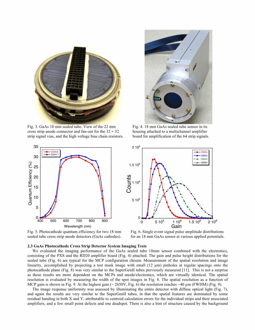
Fig. 3. GaAs 18 mm sealed tube. View of the 22 mm Fig. 4. 18 mm GaAs sealed tube sensor in its cross strip anode connector and fan-out for the 32 + 32 housing attached to a multichannel amplifier strip signal vias, and the high voltage bias chain resistors. board for amplification of the 64 strip signals.
Fig. 5. Photocathode quantum efficiency for two 18 mm Fig. 6. Single event signal pulse amplitude distributions sealed tube cross strip anode detectors (GaAs cathodes). for an 18 mm GaAs sensor at various applied potentials.
2.3 GaAs Photocathode Cross Strip Detector System Imaging Tests
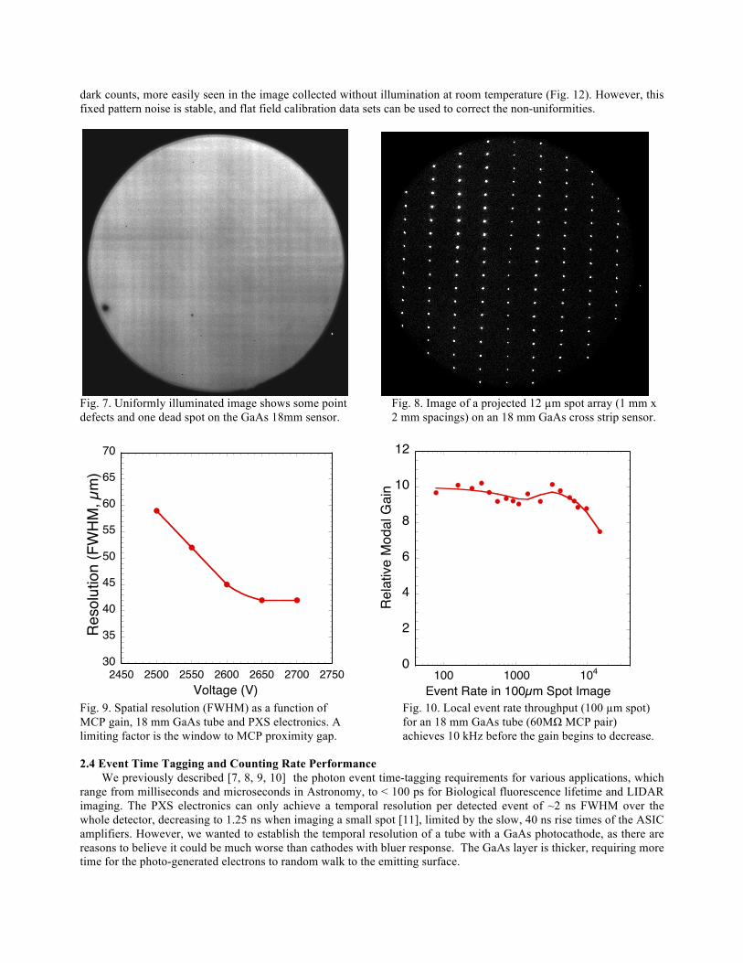
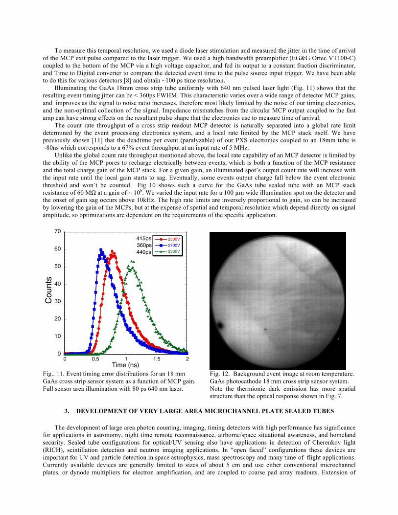
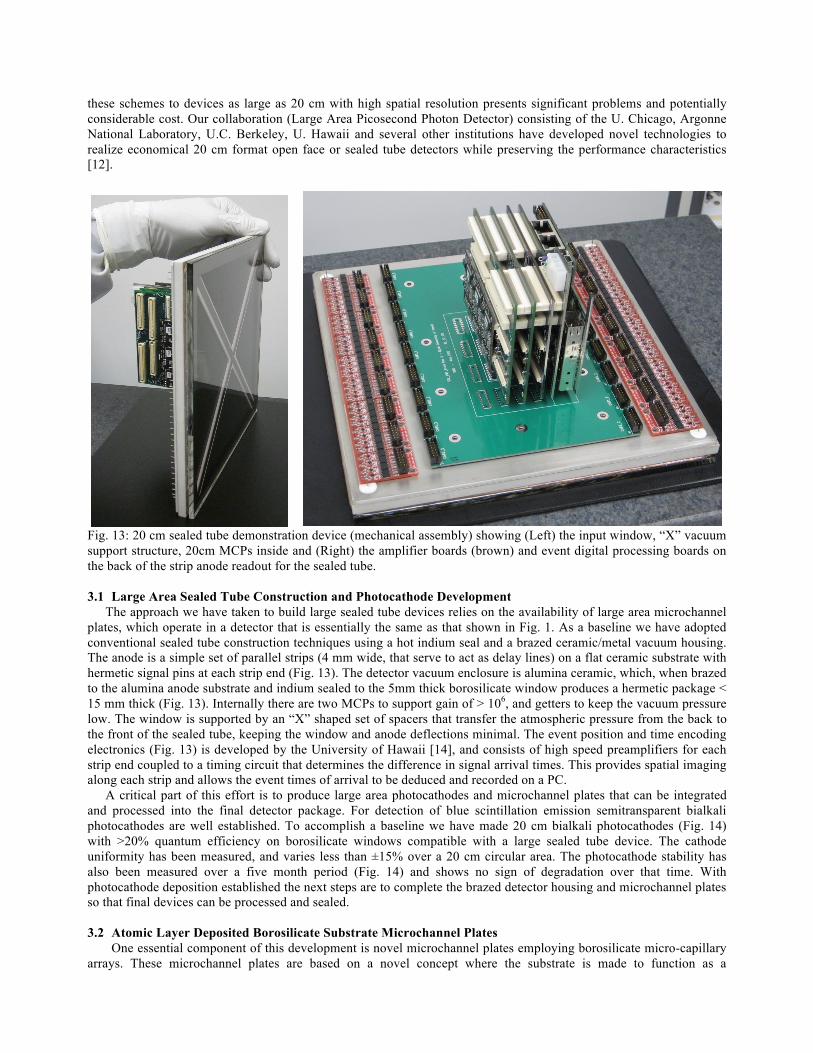
We evaluated the imaging performance of the GaAs sealed tube 18mm sensor combined with the electronics, consisting of the PXS and the RD20 amplifier board (Fig. 4) attached. The gain and pulse height distributions for the sealed tube (Fig. 6) are typical for the MCP configuration chosen. Measurement of the spatial resolution and image linearity, accomplished by projecting a test mask image with small (12 µm) pinholes at regular spacings onto the photocathode plane (Fig. 8) was very similar to the SuperGenII tubes previously measured [11]. This is not a surprise as these results are more dependent on the MCPs and anode/electronics, which are virtually identical. The spatial resolution is evaluated by measuring the width of the spot images in Fig. 8. The spatial resolution as a function of MCP gain is shown in Fig. 9. At the highest gain (~ 2650V, Fig. 6) the resolution reaches ~40 µm (FWHM) (Fig. 9).
The image response uniformity was assessed by illuminating the entire detector with diffuse optical light (Fig. 7), and again the results are very similar to the SuperGenII tubes, in that the spatial features are dominated by some residual banding in both X and Y, attributable to centroid calculation errors for the individual strips and their associated amplifiers, and a few small point defects and one deadspot. There is also a hint of structure caused by the background
0
5
10
15
20
25
30
35
400 500 600 700 800 900
GaAs3GaAs 1
Qua
ntum
Effi
cien
cy (%
)
Wavelength (nm)
0
5 105
1 106
1.5 106
2 106
0 5 105 1 106 1.5 106 2 106
2500v2550v2600v2650v
Cou
nts
Gain
dark counts, more easily seen in the image collected without illumination at room temperature (Fig. 12). However, this fixed pattern noise is stable, and flat field calibration data sets can be used to correct the non-uniformities.
Fig. 7. Uniformly illuminated image shows some point Fig. 8. Image of a projected 12 µm spot array (1 mm x defects and one dead spot on the GaAs 18mm sensor. 2 mm spacings) on an 18 mm GaAs cross strip sensor.
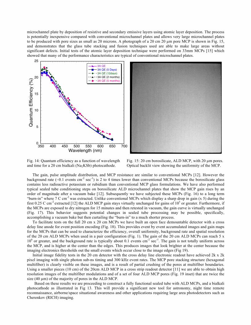
Fig. 9. Spatial resolution (FWHM) as a function of Fig. 10. Local event rate throughput (100 µm spot) MCP gain, 18 mm GaAs tube and PXS electronics. A for an 18 mm GaAs tube (60MΩ MCP pair) limiting factor is the window to MCP proximity gap. achieves 10 kHz before the gain begins to decrease. 2.4 Event Time Tagging and Counting Rate Performance
We previously described [7, 8, 9, 10] the photon event time-tagging requirements for various applications, which range from milliseconds and microseconds in Astronomy, to < 100 ps for Biological fluorescence lifetime and LIDAR imaging. The PXS electronics can only achieve a temporal resolution per detected event of ~2 ns FWHM over the whole detector, decreasing to 1.25 ns when imaging a small spot [11], limited by the slow, 40 ns rise times of the ASIC amplifiers. However, we wanted to establish the temporal resolution of a tube with a GaAs photocathode, as there are reasons to believe it could be much worse than cathodes with bluer response. The GaAs layer is thicker, requiring more time for the photo-generated electrons to random walk to the emitting surface.
30
35
40
45
50
55
60
65
70
2450 2500 2550 2600 2650 2700 2750
Res
olut
ion
(FW
HM
, µm
)
Voltage (V)
0
2
4
6
8
10
12
100 1000 104
Rel
ativ
e M
odal
Gai
n
Event Rate in 100µm Spot Image
To measure this temporal resolution, we used a diode laser stimulation and measured the jitter in the time of arrival of the MCP exit pulse compared to the laser trigger. We used a high bandwidth preamplifier (EG&G Ortec VT100-C) coupled to the bottom of the MCP via a high voltage capacitor, and fed its output to a constant fraction discriminator, and Time to Digital converter to compare the detected event time to the pulse source input trigger. We have been able to do this for various detectors [8] and obtain ~100 ps time resolution.
Illuminating the GaAs 18mm cross strip tube uniformly with 640 nm pulsed laser light (Fig. 11) shows that the resulting event timing jitter can be < 360ps FWHM. This characteristic varies over a wide range of detector MCP gains, and improves as the signal to noise ratio increases, therefore most likely limited by the noise of our timing electronics, and the non-optimal collection of the signal. Impedance mismatches from the circular MCP output coupled to the fast amp can have strong effects on the resultant pulse shape that the electronics use to measure time of arrival.
The count rate throughput of a cross strip readout MCP detector is naturally separated into a global rate limit determined by the event processing electronics system, and a local rate limited by the MCP stack itself. We have previously shown [11] that the deadtime per event (paralyzable) of our PXS electronics coupled to an 18mm tube is ~80ns which corresponds to a 67% event throughput at an input rate of 5 MHz.
Unlike the global count rate throughput mentioned above, the local rate capability of an MCP detector is limited by the ability of the MCP pores to recharge electrically between events, which is both a function of the MCP resistance and the total charge gain of the MCP stack. For a given gain, an illuminated spot’s output count rate will increase with the input rate until the local gain starts to sag. Eventually, some events output charge fall below the event electronic threshold and won’t be counted. Fig 10 shows such a curve for the GaAs tube sealed tube with an MCP stack resistance of 60 MΩ at a gain of ~ 106. We varied the input rate for a 100 µm wide illumination spot on the detector and the onset of gain sag occurs above 10kHz. The high rate limits are inversely proportional to gain, so can be increased by lowering the gain of the MCPs, but at the expense of spatial and temporal resolution which depend directly on signal amplitude, so optimizations are dependent on the requirements of the specific application.
Fig.. 11. Event timing error distributions for an 18 mm Fig. 12. Background event image at room temperature. GaAs cross strip sensor system as a function of MCP gain. GaAs photocathode 18 mm cross strip sensor system. Full sensor area illumination with 80 ps 640 nm laser. Note the thermionic dark emission has more spatial structure than the optical response shown in Fig. 7.
3. DEVELOPMENT OF VERY LARGE AREA MICROCHANNEL PLATE SEALED TUBES
The development of large area photon counting, imaging, timing detectors with high performance has significance for applications in astronomy, night time remote reconnaissance, airborne/space situational awareness, and homeland security. Sealed tube configurations for optical/UV sensing also have applications in detection of Cherenkov light (RICH), scintillation detection and neutron imaging applications. In “open faced” configurations these devices are important for UV and particle detection in space astrophysics, mass spectroscopy and many time-of–flight applications. Currently available devices are generally limited to sizes of about 5 cm and use either conventional microchannel plates, or dynode multipliers for electron amplification, and are coupled to coarse pad array readouts. Extension of
0
10
20
30
40
50
60
70
0 0.5 1 1.5 2
2500V2700V2300V
Cou
nts
Time (ns)
440ps360ps415ps
these schemes to devices as large as 20 cm with high spatial resolution presents significant problems and potentially considerable cost. Our collaboration (Large Area Picosecond Photon Detector) consisting of the U. Chicago, Argonne National Laboratory, U.C. Berkeley, U. Hawaii and several other institutions have developed novel technologies to realize economical 20 cm format open face or sealed tube detectors while preserving the performance characteristics [12].
Fig. 13: 20 cm sealed tube demonstration device (mechanical assembly) showing (Left) the input window, “X” vacuum support structure, 20cm MCPs inside and (Right) the amplifier boards (brown) and event digital processing boards on the back of the strip anode readout for the sealed tube. 3.1 Large Area Sealed Tube Construction and Photocathode Development
The approach we have taken to build large sealed tube devices relies on the availability of large area microchannel plates, which operate in a detector that is essentially the same as that shown in Fig. 1. As a baseline we have adopted conventional sealed tube construction techniques using a hot indium seal and a brazed ceramic/metal vacuum housing. The anode is a simple set of parallel strips (4 mm wide, that serve to act as delay lines) on a flat ceramic substrate with hermetic signal pins at each strip end (Fig. 13). The detector vacuum enclosure is alumina ceramic, which, when brazed to the alumina anode substrate and indium sealed to the 5mm thick borosilicate window produces a hermetic package < 15 mm thick (Fig. 13). Internally there are two MCPs to support gain of > 106, and getters to keep the vacuum pressure low. The window is supported by an “X” shaped set of spacers that transfer the atmospheric pressure from the back to the front of the sealed tube, keeping the window and anode deflections minimal. The event position and time encoding electronics (Fig. 13) is developed by the University of Hawaii [14], and consists of high speed preamplifiers for each strip end coupled to a timing circuit that determines the difference in signal arrival times. This provides spatial imaging along each strip and allows the event times of arrival to be deduced and recorded on a PC.
A critical part of this effort is to produce large area photocathodes and microchannel plates that can be integrated and processed into the final detector package. For detection of blue scintillation emission semitransparent bialkali photocathodes are well established. To accomplish a baseline we have made 20 cm bialkali photocathodes (Fig. 14) with >20% quantum efficiency on borosilicate windows compatible with a large sealed tube device. The cathode uniformity has been measured, and varies less than ±15% over a 20 cm circular area. The photocathode stability has also been measured over a five month period (Fig. 14) and shows no sign of degradation over that time. With photocathode deposition established the next steps are to complete the brazed detector housing and microchannel plates so that final devices can be processed and sealed. 3.2 Atomic Layer Deposited Borosilicate Substrate Microchannel Plates
One essential component of this development is novel microchannel plates employing borosilicate micro-capillary arrays. These microchannel plates are based on a novel concept where the substrate is made to function as a
microchannel plate by deposition of resistive and secondary emissive layers using atomic layer deposition. The process is potentially inexpensive compared with conventional microchannel plates and allows very large microchannel plates to be produced with pore sizes as small as 20 microns. A photograph of a 20 cm 20 µm pore MCP is shown in Fig. 15, and demonstrates that the glass tube stacking and fusion techniques used are able to make large areas without significant defects. Initial tests of the atomic layer deposition technique were performed on 33mm MCPs [15] which showed that many of the performance characteristics are typical of conventional microchannel plates.
Fig. 14: Quantum efficiency as a function of wavelength Fig. 15: 20 cm borosilicate, ALD MCP, with 20 µm pores. and time for a 20 cm bialkali (Na2KSb) photocathode. Optical backlit view showing the uniformity of the MCP.
The gain, pulse amplitude distribution, and MCP resistance are similar to conventional MCPs [12]. However the background rate (~0.1 events cm-2 sec-1) is 2 to 4 times lower than conventional MCPs because the borosilicate glass contains less radioactive potassium or rubidium than conventional MCP glass formulations. We have also performed typical sealed tube conditioning steps on borosilicate ALD microchannel plates that show the MCP gain rises by an order of magnitude after a vacuum bake [12]. Subsequently we have subjected these MCPs (Fig. 16) to a long term “burn-in” where 7 C cm-2 was extracted. Unlike conventional MCPs which display a sharp drop in gain (x 5) during the first 0.25 C cm-2 extracted [12] the ALD MCP gain stays virtually unchanged for gains of 105 or greater. Furthermore, if the MCPs are exposed to dry nitrogen for 15 minutes and then retested in vacuum, the gain curve is virtually unchanged (Fig. 17). This behavior suggests potential changes in sealed tube processing may be possible, specifically, accomplishing a vacuum bake but then curtailing the “burn-in” to a much shorter process.
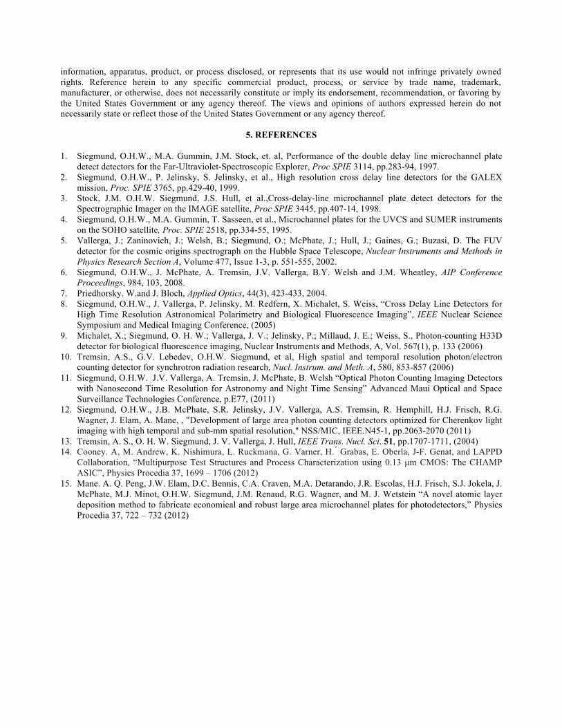
To facilitate tests on the full 20 cm x 20 cm MCPs we have built an open face demountable detector with a cross delay line anode for event position encoding (Fig. 18). This provides event by event accumulated images and gain maps for the MCPs that can be used to characterize the efficiency, overall uniformity, background rate and spatial resolution of the 20 cm ALD MCPs when used in a pair configuration (Fig. 1). The gain of the 20 cm ALD MCPs can reach 5 x 10⁶ or greater, and the background rate is typically about 0.1 events cm-2 sec-1. The gain is not totally uniform across the MCP, and is higher at the center than the edges. This produces images that look brighter at the center because the imaging electronics thresholds out the small events which occur close to the image edges (Fig 19).
Initial image fidelity tests in the 20 cm detector with the cross delay line electronic readout have achieved 2k x 2k pixel imaging with single photon sub-ns timing and 300 kHz event rates. The MCP pore stacking structure (hexagonal multifiber) is clearly visible on these images, and is a result of partial crushing of the pores at multifiber boundaries. Using a smaller pieces (10 cm) of the 20cm ALD MCP in a cross strip readout detector [11] we are able to obtain high resolution images of the multifiber modulations and of a set of four ALD MCP pores (Fig. 19 inset) that are twice the size (40 µm) of the majority of pores in the ALD MCP.
Based on these results we are proceeding to construct a fully functional sealed tube with ALD MCPs, and a bialkali photocathode as illustrated in Fig 13. This will provide a significant new tool for astronomy, night time remote reconnaissance, airborne/space situational awareness and other applications requiring large area photodetectors such as Cherenkov (RICH) imaging.
0
5
10
15
20
25
350 400 450 500 550 600 650 700
3A QE3A QE (5 Days)3A QE (12days)3A QE (2 months)3A QE (5 months)
Qua
ntum
Effi
cien
cy (%
)
Wavelength (nm)
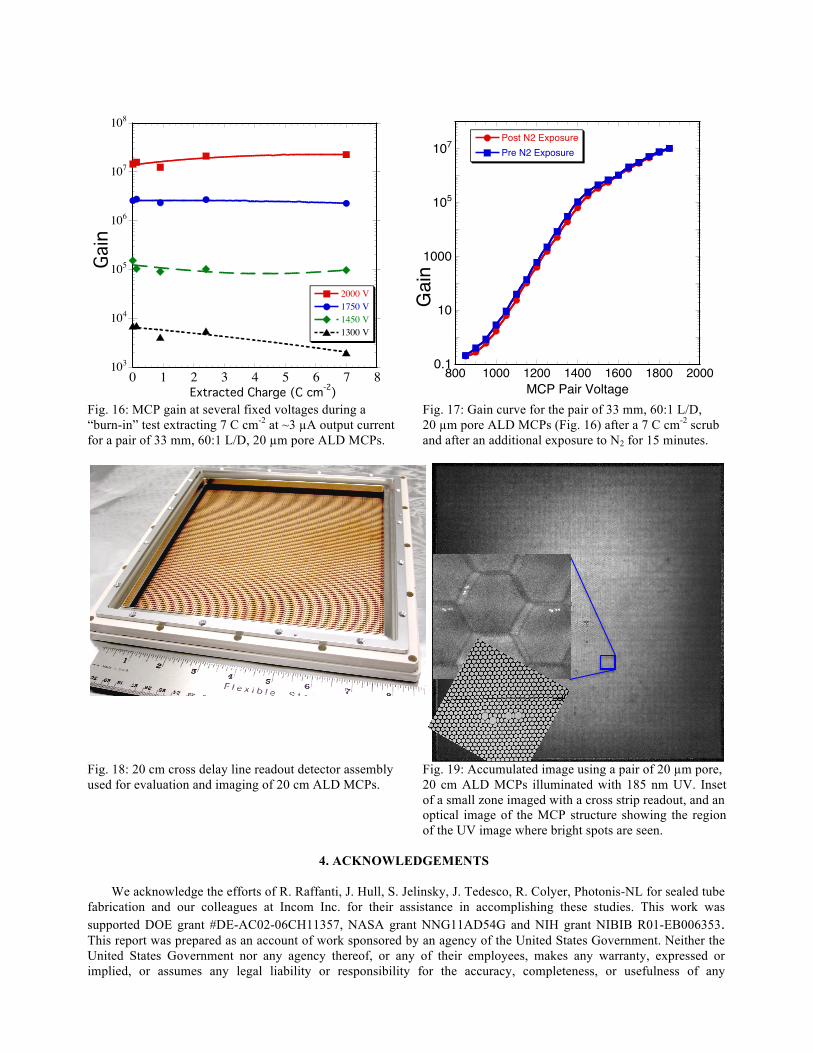
Fig. 16: MCP gain at several fixed voltages during a Fig. 17: Gain curve for the pair of 33 mm, 60:1 L/D, “burn-in” test extracting 7 C cm-2 at ~3 µA output current 20 µm pore ALD MCPs (Fig. 16) after a 7 C cm-2 scrub for a pair of 33 mm, 60:1 L/D, 20 µm pore ALD MCPs. and after an additional exposure to N2 for 15 minutes.
Fig. 18: 20 cm cross delay line readout detector assembly Fig. 19: Accumulated image using a pair of 20 µm pore, used for evaluation and imaging of 20 cm ALD MCPs. 20 cm ALD MCPs illuminated with 185 nm UV. Inset
of a small zone imaged with a cross strip readout, and an optical image of the MCP structure showing the region
of the UV image where bright spots are seen.
4. ACKNOWLEDGEMENTS
We acknowledge the efforts of R. Raffanti, J. Hull, S. Jelinsky, J. Tedesco, R. Colyer, Photonis-NL for sealed tube fabrication and our colleagues at Incom Inc. for their assistance in accomplishing these studies. This work was supported DOE grant #DE-AC02-06CH11357, NASA grant NNG11AD54G and NIH grant NIBIB R01-EB006353. This report was prepared as an account of work sponsored by an agency of the United States Government. Neither the United States Government nor any agency thereof, or any of their employees, makes any warranty, expressed or implied, or assumes any legal liability or responsibility for the accuracy, completeness, or usefulness of any
103
104
105
106
107
108
0 1 2 3 4 5 6 7 8
2000 V1750 V1450 V1300 V
Gain
Extracted Charge (C cm-2)
0.1
10
1000
105
107
800 1000 1200 1400 1600 1800 2000
Post N2 ExposurePre N2 Exposure
Gai
n
MCP Pair Voltage
information, apparatus, product, or process disclosed, or represents that its use would not infringe privately owned rights. Reference herein to any specific commercial product, process, or service by trade name, trademark, manufacturer, or otherwise, does not necessarily constitute or imply its endorsement, recommendation, or favoring by the United States Government or any agency thereof. The views and opinions of authors expressed herein do not necessarily state or reflect those of the United States Government or any agency thereof.
5. REFERENCES 1. Siegmund, O.H.W., M.A. Gummin, J.M. Stock, et. al, Performance of the double delay line microchannel plate
detect detectors for the Far-Ultraviolet-Spectroscopic Explorer, Proc SPIE 3114, pp.283-94, 1997. 2. Siegmund, O.H.W., P. Jelinsky, S. Jelinsky, et al., High resolution cross delay line detectors for the GALEX
mission, Proc. SPIE 3765, pp.429-40, 1999. 3. Stock, J.M. O.H.W. Siegmund, J.S. Hull, et al.,Cross-delay-line microchannel plate detect detectors for the
Spectrographic Imager on the IMAGE satellite, Proc SPIE 3445, pp.407-14, 1998. 4. Siegmund, O.H.W., M.A. Gummin, T. Sasseen, et al., Microchannel plates for the UVCS and SUMER instruments
on the SOHO satellite, Proc. SPIE 2518, pp.334-55, 1995. 5. Vallerga, J.; Zaninovich, J.; Welsh, B.; Siegmund, O.; McPhate, J.; Hull, J.; Gaines, G.; Buzasi, D. The FUV
detector for the cosmic origins spectrograph on the Hubble Space Telescope, Nuclear Instruments and Methods in Physics Research Section A, Volume 477, Issue 1-3, p. 551-555, 2002.
6. Siegmund, O.H.W., J. McPhate, A. Tremsin, J.V. Vallerga, B.Y. Welsh and J.M. Wheatley, AIP Conference Proceedings, 984, 103, 2008.
7. Priedhorsky. W.and J. Bloch, Applied Optics, 44(3), 423-433, 2004. 8. Siegmund, O.H.W., J. Vallerga, P. Jelinsky, M. Redfern, X. Michalet, S. Weiss, “Cross Delay Line Detectors for
High Time Resolution Astronomical Polarimetry and Biological Fluorescence Imaging”, IEEE Nuclear Science Symposium and Medical Imaging Conference, (2005)
9. Michalet, X.; Siegmund, O. H. W.; Vallerga, J. V.; Jelinsky, P.; Millaud, J. E.; Weiss, S., Photon-counting H33D detector for biological fluorescence imaging, Nuclear Instruments and Methods, A, Vol. 567(1), p. 133 (2006)
10. Tremsin, A.S., G.V. Lebedev, O.H.W. Siegmund, et al, High spatial and temporal resolution photon/electron counting detector for synchrotron radiation research, Nucl. Instrum. and Meth. A, 580, 853-857 (2006)
11. Siegmund, O.H.W. J.V. Vallerga, A. Tremsin, J. McPhate, B. Welsh “Optical Photon Counting Imaging Detectors with Nanosecond Time Resolution for Astronomy and Night Time Sensing” Advanced Maui Optical and Space Surveillance Technologies Conference, p.E77, (2011)
12. Siegmund, O.H.W., J.B. McPhate, S.R. Jelinsky, J.V. Vallerga, A.S. Tremsin, R. Hemphill, H.J. Frisch, R.G. Wagner, J. Elam, A. Mane, , "Development of large area photon counting detectors optimized for Cherenkov light imaging with high temporal and sub-mm spatial resolution," NSS/MIC, IEEE.N45-1, pp.2063-2070 (2011)
13. Tremsin, A. S., O. H. W. Siegmund, J. V. Vallerga, J. Hull, IEEE Trans. Nucl. Sci. 51, pp.1707-1711, (2004) 14. Cooney. A, M. Andrew, K. Nishimura, L. Ruckmana, G. Varner, H. ́ Grabas, E. Oberla, J-F. Genat, and LAPPD
Collaboration, “Multipurpose Test Structures and Process Characterization using 0.13 µm CMOS: The CHAMP ASIC”, Physics Procedia 37, 1699 – 1706 (2012)
15. Mane. A. Q. Peng, J.W. Elam, D.C. Bennis, C.A. Craven, M.A. Detarando, J.R. Escolas, H.J. Frisch, S.J. Jokela, J. McPhate, M.J. Minot, O.H.W. Siegmund, J.M. Renaud, R.G. Wagner, and M. J. Wetstein “A novel atomic layer deposition method to fabricate economical and robust large area microchannel plates for photodetectors,” Physics Procedia 37, 722 – 732 (2012)