Embed Size (px)
Citation preview

Labs
Some of these labs are adapted from Clint Cole's Real Digital, published by Digilent.
Your incentive to complete the labs (besides love of learning, and the fact that they're
kind of fun) is that the tests will include Verilog and may cover specific details taught only
through these labs.
We use the Xilinx ISE software to describe and simulate our circuits, and to generate the
programming file for the FPGA. If you'd like to work outside the lab, you may download
a free (WebPACK) version of this software from
http://www.xilinx.com/support/download/index.html/content/xilinx/en/downloadNav/desig
n-tools.html.
We use the Digilent Adept software to load the programming files onto our FPGAs. I'd
prefer to leave the FPGA boards in the lab, so you don't need to install Digilent Adept on
your own computer.

Lab 1 Names:
Introduction
In this lab project, you will download a .bit file to your board to configure the FPGA with eight
different logic circuits. The circuits use buttons and switches for inputs, and LEDs for outputs.
You must probe the logic circuits by applying all possible combinations of input signals, and
from the results write logic equations that describe the circuit’s behavior.
Set the blue "jumper" in the upper right corner of your board to PC mode.
Obtain the file “lab1_Basys2.bit” from
https://learn.digilentinc.com/Classroom/RealDigital/M2/Lab1BitFiles.zip, and download it to your
Basys 2 Digilent board using the Digilent Adept software. (Click Browse to find the file, then
Program. Click Yes in response to any warning messages.) Your board will be configured with
eight logic circuits that drive the eight on-board LEDs. You must find logic equations to describe
the circuits. After the FPGA is configured with the bit file, apply all combinations of relevant
inputs (hint: see the input variable names on the top row of each truth table), and use the output
LED status to complete the following truth tables. Write a logic assignment equation that shows
the behavior of each circuit (the equations do not need to be minimum).
swt7 btn3 LED7
0 0
0 1
1 0
1 1
LED7 =
swt6 btn3 LED6
0 0
0 1
1 0
1 1
LED6 =
swt7 swt6 swt5 LED5
0 0 0
0 0 1
0 1 0
0 1 1
1 0 0
1 0 1
1 1 0
1 1 1
LED5 =
btn3 btn2 LED4
0 0
0 1
1 0
1 1
LED4 =
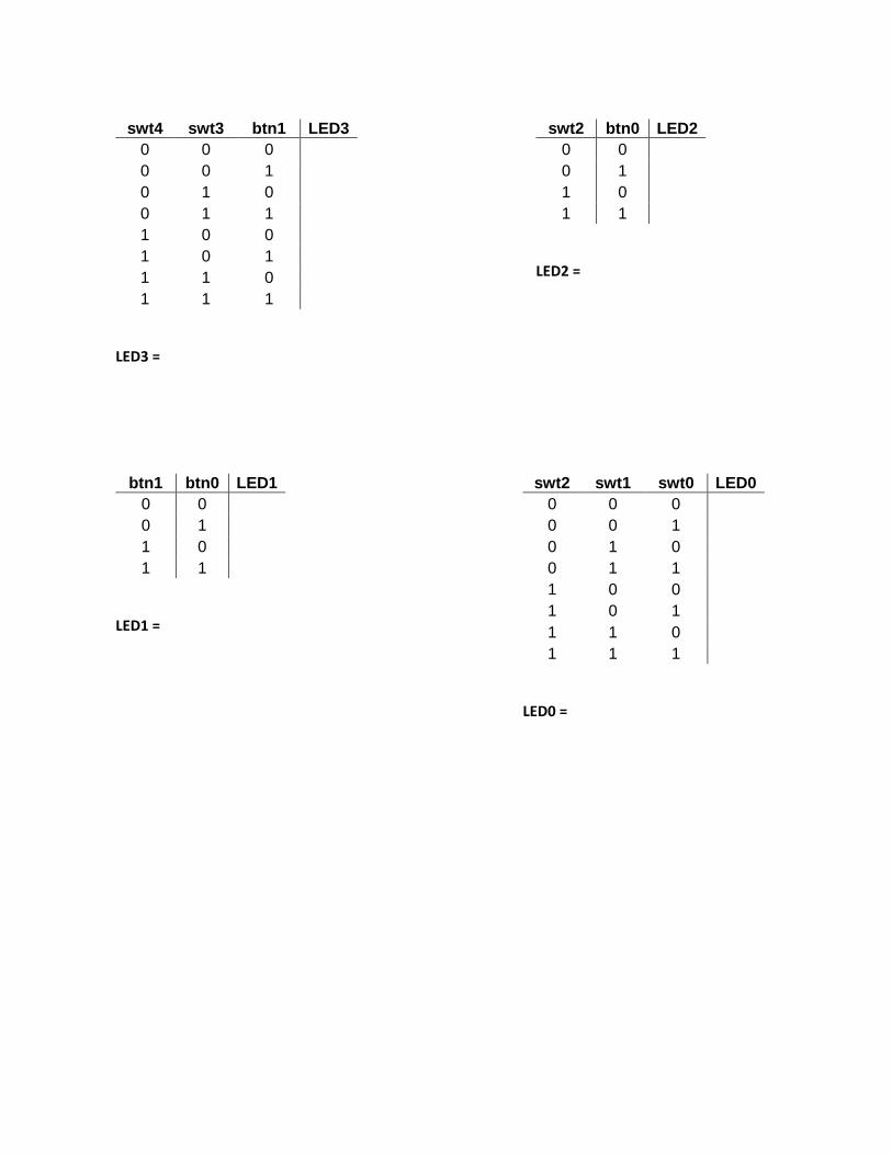
swt4 swt3 btn1 LED3
0 0 0
0 0 1
0 1 0
0 1 1
1 0 0
1 0 1
1 1 0
1 1 1
LED3 =
swt2 btn0 LED2
0 0
0 1
1 0
1 1
LED2 =
btn1 btn0 LED1
0 0
0 1
1 0
1 1
LED1 =
swt2 swt1 swt0 LED0
0 0 0
0 0 1
0 1 0
0 1 1
1 0 0
1 0 1
1 1 0
1 1 1
LED0 =
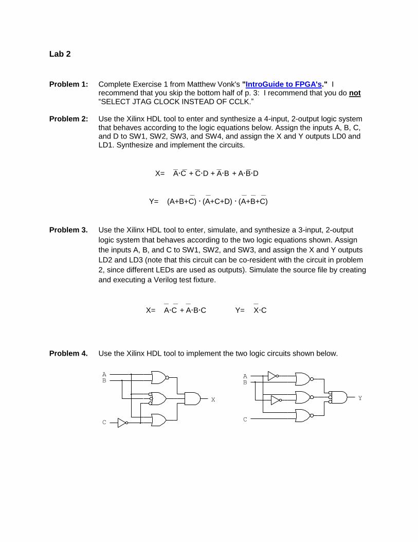
Lab 2
Problem 1: Complete Exercise 1 from Matthew Vonk's "IntroGuide to FPGA's." I
recommend that you skip the bottom half of p. 3: I recommend that you do not “SELECT JTAG CLOCK INSTEAD OF CCLK.”
Problem 2: Use the Xilinx HDL tool to enter and synthesize a 4-input, 2-output logic system
that behaves according to the logic equations below. Assign the inputs A, B, C, and D to SW1, SW2, SW3, and SW4, and assign the X and Y outputs LD0 and LD1. Synthesize and implement the circuits.
Problem 3. Use the Xilinx HDL tool to enter, simulate, and synthesize a 3-input, 2-output
logic system that behaves according to the two logic equations shown. Assign
the inputs A, B, and C to SW1, SW2, and SW3, and assign the X and Y outputs
LD2 and LD3 (note that this circuit can be co-resident with the circuit in problem
2, since different LEDs are used as outputs). Simulate the source file by creating
and executing a Verilog test fixture.
Problem 4. Use the Xilinx HDL tool to implement the two logic circuits shown below.
X= AC + CD + AB + ABD __ __ __ __ __
__ __ __ __ __
Y= (A+B+C) (A+C+D) (A+B+C)
__ __ __ __
X= AC + ABC Y= XC
BA
C
X
BA
C
Y
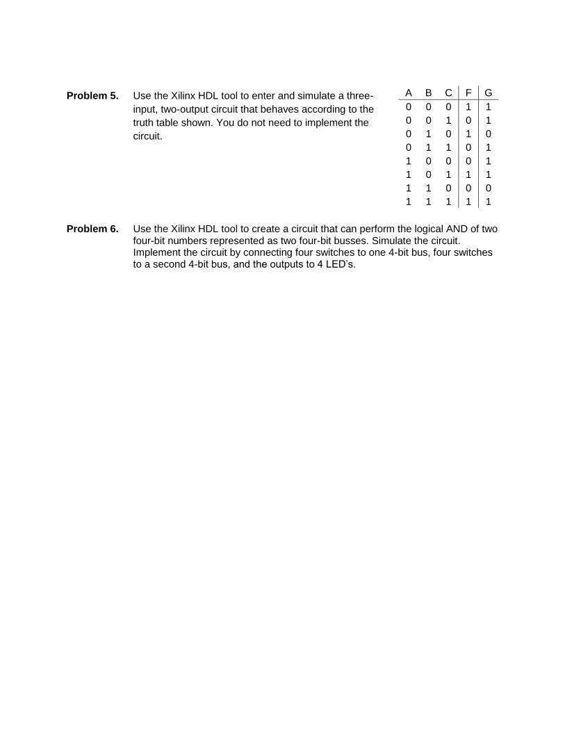
Problem 5. Use the Xilinx HDL tool to enter and simulate a three-
input, two-output circuit that behaves according to the
truth table shown. You do not need to implement the
circuit.
Problem 6. Use the Xilinx HDL tool to create a circuit that can perform the logical AND of two
four-bit numbers represented as two four-bit busses. Simulate the circuit. Implement the circuit by connecting four switches to one 4-bit bus, four switches to a second 4-bit bus, and the outputs to 4 LED’s.
A B C F G
0 0 0 1 1
0 0 1 0 1
0 1 0 1 0
0 1 1 0 1
1 0 0 0 1
1 0 1 1 1
1 1 0 0 0
1 1 1 1 1
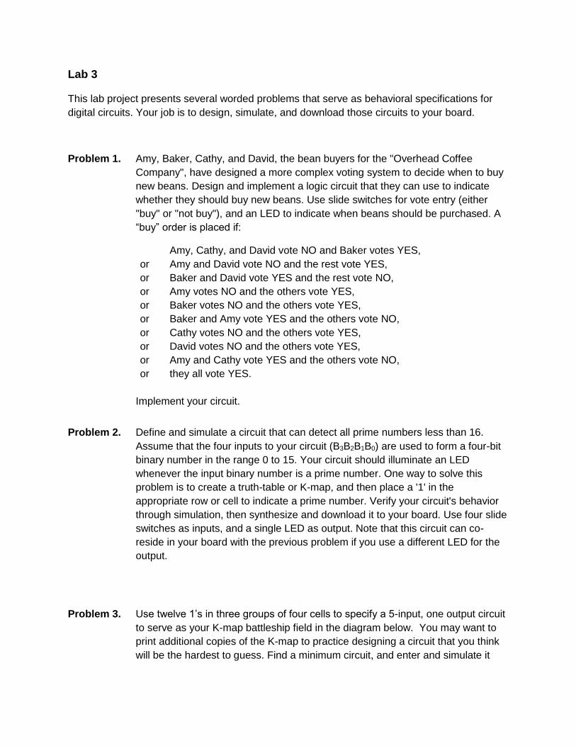
Lab 3 This lab project presents several worded problems that serve as behavioral specifications for
digital circuits. Your job is to design, simulate, and download those circuits to your board.
Problem 1. Amy, Baker, Cathy, and David, the bean buyers for the "Overhead Coffee
Company", have designed a more complex voting system to decide when to buy
new beans. Design and implement a logic circuit that they can use to indicate
whether they should buy new beans. Use slide switches for vote entry (either
"buy" or "not buy"), and an LED to indicate when beans should be purchased. A
“buy” order is placed if:
Amy, Cathy, and David vote NO and Baker votes YES,
or Amy and David vote NO and the rest vote YES,
or Baker and David vote YES and the rest vote NO,
or Amy votes NO and the others vote YES,
or Baker votes NO and the others vote YES,
or Baker and Amy vote YES and the others vote NO,
or Cathy votes NO and the others vote YES,
or David votes NO and the others vote YES,
or Amy and Cathy vote YES and the others vote NO,
or they all vote YES.
Implement your circuit.
Problem 2. Define and simulate a circuit that can detect all prime numbers less than 16.
Assume that the four inputs to your circuit (B3B2B1B0) are used to form a four-bit
binary number in the range 0 to 15. Your circuit should illuminate an LED
whenever the input binary number is a prime number. One way to solve this
problem is to create a truth-table or K-map, and then place a '1' in the
appropriate row or cell to indicate a prime number. Verify your circuit's behavior
through simulation, then synthesize and download it to your board. Use four slide
switches as inputs, and a single LED as output. Note that this circuit can co-
reside in your board with the previous problem if you use a different LED for the
output.
Problem 3. Use twelve 1’s in three groups of four cells to specify a 5-input, one output circuit
to serve as your K-map battleship field in the diagram below. You may want to
print additional copies of the K-map to practice designing a circuit that you think
will be the hardest to guess. Find a minimum circuit, and enter and simulate it
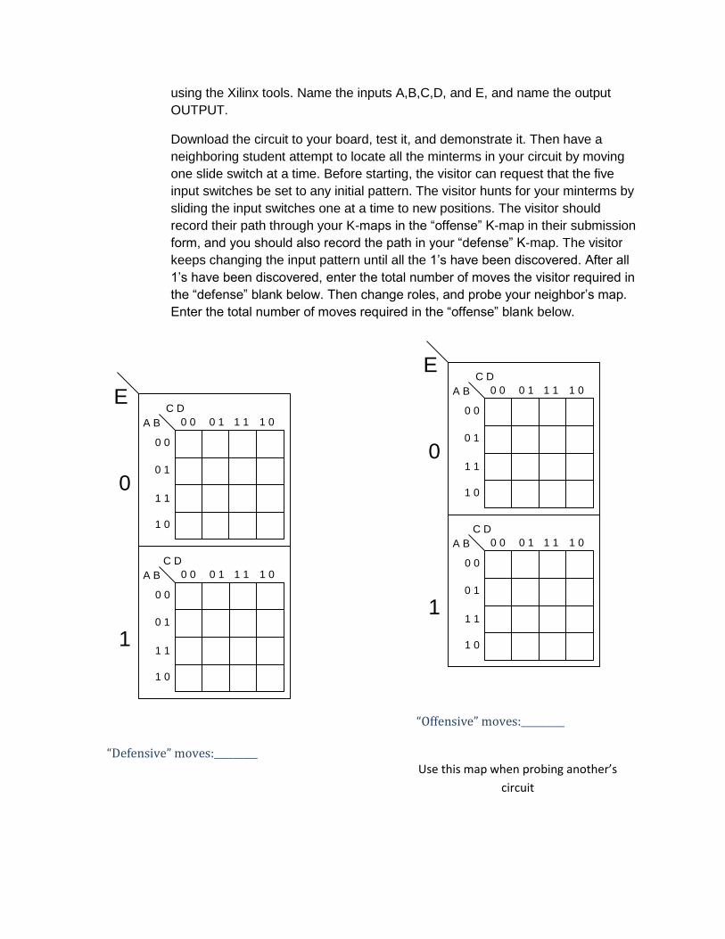
using the Xilinx tools. Name the inputs A,B,C,D, and E, and name the output
OUTPUT.
Download the circuit to your board, test it, and demonstrate it. Then have a
neighboring student attempt to locate all the minterms in your circuit by moving
one slide switch at a time. Before starting, the visitor can request that the five
input switches be set to any initial pattern. The visitor hunts for your minterms by
sliding the input switches one at a time to new positions. The visitor should
record their path through your K-maps in the “offense” K-map in their submission
form, and you should also record the path in your “defense” K-map. The visitor
keeps changing the input pattern until all the 1’s have been discovered. After all
1’s have been discovered, enter the total number of moves the visitor required in
the “defense” blank below. Then change roles, and probe your neighbor’s map.
Enter the total number of moves required in the “offense” blank below.
A B
C D
0 0 0 1 1 1 1 0
0 0
0 1
1 1
1 0
A B
C D
0 0 0 1 1 1 1 0
0 0
0 1
1 1
1 0
E
0
1
“Defensive” moves:_________
Use this map when someone else is
probing your circuit
A B
C D
0 0 0 1 1 1 1 0
0 0
0 1
1 1
1 0
A B
C D
0 0 0 1 1 1 1 0
0 0
0 1
1 1
1 0
E
0
1
“Offensive” moves:_________
Use this map when probing another’s
circuit

Lab 4 This lab project presents several more complex combinational logic systems that would be quite
challenging to implement using structural methods, but are rather simple using Verilog.
Problem 1: Six judges need a device to help indicate particular judgments. Each judge can
enter “good” or “bad” with a single switch - you job is to build a circuit that can indicate three separate conditions: A strong majority (i.e., 5 or 6 “good” votes); a simple majority (4 or more “good” votes), and a tie (exactly 3 “good” votes). Use LEDs to indicate the outputs.
Problem 2. A digital thermometer produces a continuously varying voltage signal between
0V and 5V, where 0V represents 0 degrees, and 5V represents 100 degrees.
The thermometer outputs an 8-bit binary number proportional to the temperature
– “00000000” represents 0 degrees, each increasing binary number from
“00000000” represents a temperature increase of 100/256 degrees, and
“11111111” represents 100 degrees. Design a circuit that outputs a logic high
signal whenever the temperature is between 50 and 60 degrees. Use switches to
emulate the thermometer's output, and an LED to indicate when the temperature
is in the desired range.
Problem 3. Design a circuit that can show an 8-bit 2's complement number multiplied by -1.
Use the eight slide switches to enter any number (positive or negative), and show
the answer on the 8 LED's.

Lab 5
Problem 1. Use the Xilinx tools to define and simulate an 8-bit shifter that can shift or rotate
left or right by 0, 1, 2, or 3 bit positions. Implement the circuit using the 8 slide switches as inputs to the shifter, and 8 LEDs as outputs from the shifter. Use the pushbuttons to control the functions of the shifter.
Problem 2. Design and simulate an 8-bit magnitude comparator.
Problem 3. Design and simulate a behavioral 8-bit adder that can produce a 9-bit result.
Show a case where the ninth bit is a '1'.
Problem 4: Design and implement a 4-bit ALU that can perform the
operations shown. Assign inputs to slide switches and pushbuttons as you see fit, and assign outputs to LEDs or the 7sd.
Op Code Function
000 A PLUS B
001 A PLUS 1
010 A MINUS B
011 A MINUS 1
100 A XOR B
101 Not A
110 A OR B
111 A AND B

Lab 6
Problem 1. Build a 4-bit binary counter with Enable and Terminal Count functions (Terminal
Count, or TC, is asserted in the last count state before the counter resets back to
all zeros). Simulate the counter, showing the TC and Enable functions.
Problem 2. Design a circuit that increments a digit (0 – F) shown on the seven-segment
display device once each second. The circuit has four pushbutton inputs: one
button starts the counter, a second button stops the counter, a third button
increments the counter, and the fourth button asynchronously resets all memory
devices in the design. The system has the block diagram shown below. Use the
4-bit counter from problem #1 as a component, and create components for a
clock divider, seven-segment display decoder, and a controller circuit.
Start
Controller
Stop
Inc
RSTClk
Run
4-bit counter
B0
B1
B2
B3
Cen
7-seg decoder
BTN1
BTN2
BTN3
BTN4
CA
CB
CC
CD
CE
CG
CF
RST
ClkClk pin
Clk divider
Problem 3. Build a 4-digit decimal stopwatch, with the least-significant digit counting a rate of
1KHz (1ms update rate), and the most-significant digit incrementing once per
second (each digit on the seven-segment display will be driven from a separate
decimal counter). Use the same controller as was used for Problem 2.
This circuit requires a scanning display controller which is discussed in your
board’s Reference Manual.

Lab 7 Problem 1: Design and implement a Mealy machine to detect the sequence 1101. Observe
the difference between a combinational output and a latched output. Problem 2: Design and implement a Moore machine to detect the sequence 110. Make sure
it works!
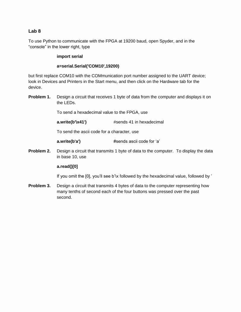
Lab 8
To use Python to communicate with the FPGA at 19200 baud, open Spyder, and in the
“console” in the lower right, type
import serial
a=serial.Serial('COM10',19200)
but first replace COM10 with the COMmunication port number assigned to the UART device;
look in Devices and Printers in the Start menu, and then click on the Hardware tab for the
device.
Problem 1. Design a circuit that receives 1 byte of data from the computer and displays it on
the LEDs.
To send a hexadecimal value to the FPGA, use
a.write(b'\x41') #sends 41 in hexadecimal
To send the ascii code for a character, use
a.write(b'a') #sends ascii code for ‘a’
Problem 2. Design a circuit that transmits 1 byte of data to the computer. To display the data
in base 10, use
a.read()[0]
If you omit the [0], you’ll see b’\x followed by the hexadecimal value, followed by ’
Problem 3. Design a circuit that transmits 4 bytes of data to the computer representing how
many tenths of second each of the four buttons was pressed over the past
second.
Lab 9
Problem 1. Create a circuit that displays the greatest common divisor of two four-bit numbers
read from a Verilog ROM (Example 68 from the book).
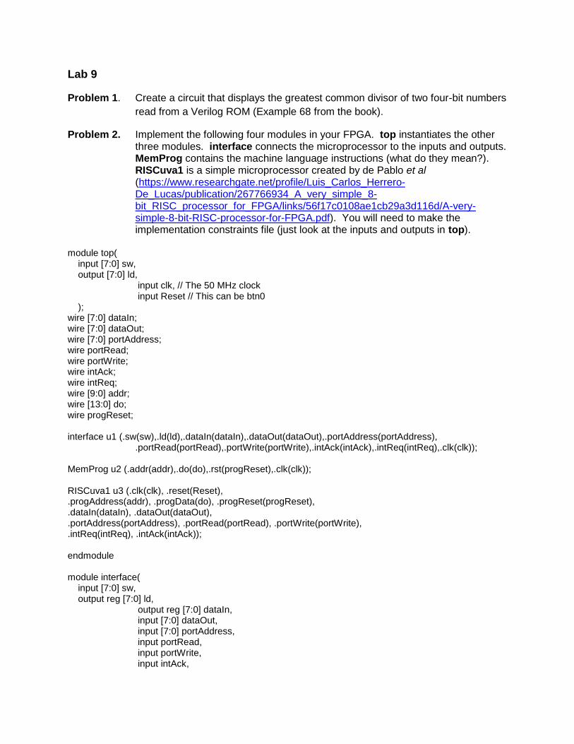
Problem 2. Implement the following four modules in your FPGA. top instantiates the other three modules. interface connects the microprocessor to the inputs and outputs. MemProg contains the machine language instructions (what do they mean?). RISCuva1 is a simple microprocessor created by de Pablo et al (https://www.researchgate.net/profile/Luis_Carlos_Herrero-De_Lucas/publication/267766934_A_very_simple_8-bit_RISC_processor_for_FPGA/links/56f17c0108ae1cb29a3d116d/A-very-simple-8-bit-RISC-processor-for-FPGA.pdf). You will need to make the implementation constraints file (just look at the inputs and outputs in top).
module top( input [7:0] sw, output [7:0] ld, input clk, // The 50 MHz clock input Reset // This can be btn0 ); wire [7:0] dataIn; wire [7:0] dataOut; wire [7:0] portAddress; wire portRead; wire portWrite; wire intAck; wire intReq; wire [9:0] addr; wire [13:0] do; wire progReset; interface u1 (.sw(sw),.ld(ld),.dataIn(dataIn),.dataOut(dataOut),.portAddress(portAddress), .portRead(portRead),.portWrite(portWrite),.intAck(intAck),.intReq(intReq),.clk(clk)); MemProg u2 (.addr(addr),.do(do),.rst(progReset),.clk(clk)); RISCuva1 u3 (.clk(clk), .reset(Reset), .progAddress(addr), .progData(do), .progReset(progReset), .dataIn(dataIn), .dataOut(dataOut), .portAddress(portAddress), .portRead(portRead), .portWrite(portWrite), .intReq(intReq), .intAck(intAck)); endmodule module interface( input [7:0] sw, output reg [7:0] ld, output reg [7:0] dataIn, input [7:0] dataOut, input [7:0] portAddress, input portRead, input portWrite, input intAck,
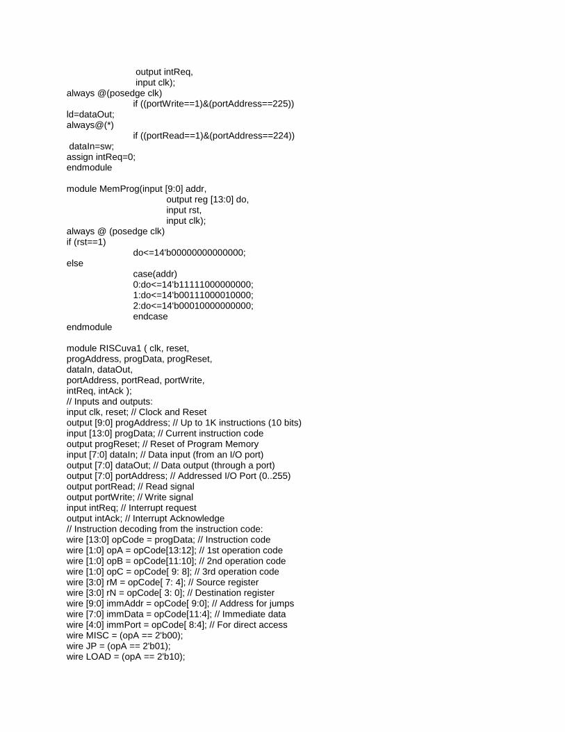
output intReq, input clk); always @(posedge clk) if ((portWrite==1)&(portAddress==225)) ld=dataOut; always@(*) if ((portRead==1)&(portAddress==224)) dataIn=sw; assign intReq=0; endmodule module MemProg(input [9:0] addr, output reg [13:0] do, input rst, input clk); always @ (posedge clk) if (rst==1) do<=14'b00000000000000; else case(addr) 0:do<=14'b11111000000000; 1:do<=14'b00111000010000; 2:do<=14'b00010000000000; endcase endmodule module RISCuva1 ( clk, reset, progAddress, progData, progReset, dataIn, dataOut, portAddress, portRead, portWrite, intReq, intAck ); // Inputs and outputs: input clk, reset; // Clock and Reset output [9:0] progAddress; // Up to 1K instructions (10 bits) input [13:0] progData; // Current instruction code output progReset; // Reset of Program Memory input [7:0] dataIn; // Data input (from an I/O port) output [7:0] dataOut; // Data output (through a port) output [7:0] portAddress; // Addressed I/O Port (0..255) output portRead; // Read signal output portWrite; // Write signal input intReq; // Interrupt request output intAck; // Interrupt Acknowledge // Instruction decoding from the instruction code: wire [13:0] opCode = progData; // Instruction code wire [1:0] opA = opCode[13:12]; // 1st operation code wire [1:0] opB = opCode[11:10]; // 2nd operation code wire [1:0] opC = opCode[ 9: 8]; // 3rd operation code wire [3:0] rM = opCode[ 7: 4]; // Source register wire [3:0] rN = opCode[ 3: 0]; // Destination register wire [9:0] immAddr = opCode[ 9:0]; // Address for jumps wire [7:0] immData = opCode[11:4]; // Immediate data wire [4:0] immPort = opCode[ 8:4]; // For direct access wire MISC = (opA == 2'b00); wire JP = (opA == 2'b01); wire LOAD = (opA == 2'b10);

wire ALU = (opA == 2'b11); wire CALL = (opB == 2'b00); wire GOTO = (opB == 2'b01); wire RETS = (opB == 2'b10); wire MOVOUT = (opB == 2'b11); wire RET = (opC == 2'b00); wire RETI = (opC == 2'b01); wire DI = (opC == 2'b10); wire EI = (opC == 2'b11); wire FLAG_Z = (opB == 2'b00); wire FLAG_NZ = (opB == 2'b01); wire FLAG_C = (opB == 2'b10); wire FLAG_NC = (opB == 2'b11); wire LOGIC = (opB == 2'b00); wire ARITH = (opB == 2'b01); wire SHIFT = (opB == 2'b10); wire MOVIN = (opB == 2'b11); wire MOV = (opC == 2'b00); wire XNOR = (opC == 2'b01); wire OR = (opC == 2'b10); wire AND = (opC == 2'b11); wire ADD = (opC == 2'b00); wire ADC = (opC == 2'b01); wire SUB = (opC == 2'b10); wire SBC = (opC == 2'b11); wire ASR = (opC == 2'b00); wire RRC = (opC == 2'b01); wire ROR = (opC == 2'b10); wire ROL = (opC == 2'b11); wire IND = (opC == 2'b00); wire SEQ = (opC == 2'b01); wire DIR = (opC >= 2'b10); // General Resources: reg zeroFlag, carryFlag; // DFFs used by flags wire [7:0] dataBus; // Data bus for all operations wire [2+9:0] stackValue; // Internal stack output // Register file (r0-r15) and operand buses: reg [7:0] registerFile[0:15]; // 16x8 dual-port memory always@(posedge clk) begin if (LOAD | ALU) registerFile[rN] <= dataBus; // Synchronous write end wire [7:0] busN = registerFile[rN]; // Async. read of rN wire [7:0] busM = registerFile[rM]; // Async. read of rM // Port signals for direct, indirect and sequential accesses: reg [7:0] nextPort; always@(posedge clk) begin if (portRead | portWrite) nextPort <= portAddress + 1; // For sequential use end assign dataOut = busN; // Output from rN assign portRead = ALU & MOVIN; // Read signal assign portWrite = MISC & MOVOUT; // Write signal assign portAddress = IND ? busM : // Indirect

SEQ ? nextPort : // Sequent. {3'b111,immPort}; // Direct // Logic ALU: AND, OR, XNOR and MOV. wire logicCarry = AND ? 1'b1 : OR ? 1'b0 : carryFlag; wire [7:0] logicALU = AND ? busN & busM : OR ? busN | busM : XNOR ? busN ~^ busM : busM ; // Arithmetic ALU: ADD, ADC, SUB and SBC. wire [7:0] arithALU, altM; wire arithCarry, x, y, z; assign x = ADD ? 1'b0 : ADC ? carryFlag : SUB ? 1'b1 : ~carryFlag; assign altM = (SUB | SBC) ? ~busM : busM; assign {z, arithALU, y} = {busN, 1'b1} + {altM, x}; assign arithCarry = (SUB | SBC) ? ~z : z; // Shifter: ASR, RRC, ROR and ROL. wire [7:0] shiftALU; wire shiftCarry; assign {shiftALU, shiftCarry} = ASR ? {busN[7], busN} : RRC ? {carryFlag, busN} : ROR ? {busN[0], busN} : {busN[6:0], busN[7], busN[7]}; // This data bus collects results from all sources: assign dataBus = (LOAD | MISC) ? immData : 8'bz; assign dataBus = (ALU | JP) & LOGIC ? logicALU : 8'bz; assign dataBus = (ALU | JP) & ARITH ? arithALU : 8'bz; assign dataBus = (ALU | JP) & SHIFT ? shiftALU : 8'bz; assign dataBus = (ALU | JP) & MOVIN ? dataIn : 8'bz; // Interrupt Controller: reg userEI, callingIRQ, intAck; wire mayIRQ = ! (MISC & RETS | MISC & MOVOUT | ALU & MOVIN); wire validIRQ = intReq & ~intAck & userEI & mayIRQ; wire [9:0] destIRQ = callingIRQ ? 10'h001 : 10'h000; always@(posedge clk or posedge reset) begin if (reset) userEI <= 0; else if (MISC & RETS & DI) userEI <= 0; else if (MISC & RETS & EI) userEI <= 1; if (reset) intAck <= 0; else if (validIRQ) intAck <= 1; else if (MISC & RETS & RETI) intAck <= 0; if (reset) callingIRQ <= 0; else callingIRQ <= validIRQ; end // Flag DFFs: always@(posedge clk) begin if (MISC & RETS & RETI) // Flags recovery when ‘reti’ {carryFlag,zeroFlag} <= stackValue[11:10]; else begin if (LOAD | ALU) // 'Z' changes with registers zeroFlag <= (dataBus == 8'h00);

if (ALU & ~MOVIN) // but 'C' only with ALU ops carryFlag <= LOGIC ? logicCarry : SHIFT ? shiftCarry : arithCarry ; end end // 'validFlag' evaluates one of four conditions for jumps. wire validFlag = FLAG_Z ? zeroFlag : FLAG_NZ ? ~zeroFlag : FLAG_C ? carryFlag : ~carryFlag ; // Program Counter (PC): the address of current instruction. reg [9:0] PC; wire [9:0] nextPC, incrPC; wire onRet = MISC & RETS & (RETI|RET); wire onJump = MISC & (GOTO | CALL) | JP & validFlag; assign incrPC = PC + (callingIRQ ? 0 : 1); assign nextPC = onRet ? stackValue[9:0] : 10'bz; assign nextPC = onJump ? immAddr | destIRQ : 10'bz; assign nextPC = !(onRet | onJump) ? incrPC : 10'bz; always@(posedge clk) begin PC <= nextPC; end // When using Xilinx BlockRAM as program memory: assign progAddress = nextPC; assign progReset = reset | validIRQ; // Internal stack for returning addresses (16 levels): reg [3:0] SP; // Stack Pointer register always@(posedge clk or posedge reset) begin if (reset) SP <= 0; else if (MISC & CALL) SP <= SP + 1; else if (MISC & RETS & (RETI|RET)) SP <= SP - 1; end wire [3:0] mySP = (CALL | GOTO) ? SP : SP - 1; reg [2+9:0] stackMem[0:15]; // Stack 16x12 memory always@(posedge clk) begin if (MISC & CALL) // Keep returning address and flags stackMem [mySP] <= {carryFlag, zeroFlag, incrPC}; end assign stackValue = stackMem[mySP]; endmodule /// RISCuva1 (all in one file!)
Problem 3. Modify the instructions in MemProg so that the output will equal the input plus 1.
You will need to store the number 1 in a register and then add.
Problem 4. Now modify the instructions so that the output equals the slide-switch input
unless BTN1 is pushed, in which case the output becomes 0. You will need to
modify top (adding an input) and interface. You must assign BTN1 (preceded
by 7 zeros) a different port number than the slide switches.