Embed Size (px)
Citation preview

Volume 12 | N
umber 13 | 2012
Lab on a Chip
Pages 2279–2426 1473-0197(2012)12:13;1-#
ISSN 1473-0197
Lab on a ChipMiniaturisation for chemistry, physics, biology, materials science and bioengineering
www.rsc.org/loc
OFC COVER SCAN
TO FIT INTO THIS BOX
www.rsc.org/locRegistered Charity Number 207890
Featuring work from the Nano-Bio Lab of Professor
Samir M. Iqbal in the Departments of Electrical
Engineering and Bioengineering, and Nanotechnology
Research & Education Center at the University of Texas
at Arlington, Arlington, Texas, USA.
Title: Electrical fi ngerprinting, 3D profi ling and detection of
tumor cells with solid-state micropores
A simple approach using solid-state micropores to diff erentiate cancer cells from blood samples. The high detection effi ciency stems from the direct measurement of mechanical and visco-elastic properties of cells that diff er between cell populations. The system has potential applications for early detection of many other diseases.
PAPER Weiming Li et al.Superelastic metal microsprings as fl uidic sensors and actuators
As featured in:
See Waseem Asghar et al., Lab Chip, 2012, 12, 2349.
RSC cover012013_DIGITAL.indd 1RSC cover012013_DIGITAL.indd 1 6/4/2012 9:21:06 AM6/4/2012 9:21:06 AM
Volume 12 | Number 13 | 7 July 2012 | Pages 2279–2422
Publ
ishe
d on
20
Mar
ch 2
012.
Dow
nloa
ded
by F
udan
Uni
vers
ity o
n 27
/02/
2018
08:
39:4
8.
View Article Online / Journal Homepage / Table of Contents for this issue

Superelastic metal microsprings as fluidic sensors and actuators{
Weiming Li,{a Gaoshan Huang,{*a Jiao Wang,a Ying Yu,a Xiaojing Wu,*a Xugao Cuib and Yongfeng Mei*ac
Received 12th February 2012, Accepted 13th March 2012
DOI: 10.1039/c2lc40151g
Superelastic metal microsprings fabricated by deterministic rolling of nanomembranes have been
anisotropic-strain-engineered via glancing angle deposition. The advantageous applications of metal
microsprings in liquid flow rate sensors and chemical-stimulated actuators due to their reliable
superelasticity are demonstrated. Theoretical calculation of microspring elongation as a function of
flow rate agrees with our experimental observation and reveals that the sensitivity can be well tuned
by the geometrical design of the microsprings. Such outstanding mechanical properties of rolled-up
metal microsprings should find important applications in future fluidic micro-/nano-devices.
Introduction
Motivated by enormous progress in the miniaturization of
mechanical, electronic, and opto-electronic devices, researchers
in micro-/nano-sciences have put great effort into the fabrication
and characterization of novel micro-/nano-structures.1–3 Typical
structures in the forms of dots,4 wires,5 tubes,6,7 etc. have been
intensively investigated in recent years and their potential
applications in drug-delivery,8 sensing,9,10 optics,11 micro swim-
mers,12 and data storage13 are being widely explored and
developed. Among various micro-/nano-structures, springs or
helices have drawn extensive research interest due to their unique
three-dimensional geometry. Compared with simpler shapes,
their structural complexities are more attractive because such
geometry may have a remarkable effect upon their physical and
chemical properties.14–16 The excellent performance of devices
consisting of micro-/nano-springs has already led to advanta-
geous uses in micro-/nano-electromechanical systems,17 targeted
delivery,18 sensing19,20 and microelectronics.21
During the past few years, micro-/nano-springs have been
fabricated from various materials, such as ZnO,22 Si3N4,23 C,24
and SiO225 via bottom-up methods e.g. solid–vapor process and
chemical vapor deposition.22,23,26 These structures are formed
entirely through a self-assembly process and thus exhibit slightly
less controllability. Recently, rolled-up nanotechnology, which
exploits both bottom-up and top-down methods,27 has been
employed to fabricate three-dimensional structures by the
rolling-up of pre-strained nanomembranes upon release from a
sacrificial layer. In the beginning, this strain was introduced to
bi-layered nanomembranes with a crystal lattice mismatch.28,29
These materials systems such as InGaAs/GaAs bilayers and
SiGe/Si bilayers were grown by chemical vapor deposition or by
molecular beam epitaxy onto sacrificial layers.6,19,30 For single-
crystal semiconductor nanomembranes, Young’s modulus is
strongly anisotropic and nanomembranes with well-defined
geometries will roll along the direction where Young’s modulus
is the smallest.30 If the orientation of a nanomembrane strip
deviates from this rolling direction, a helical structure is thus
formed, which is in fact a special case of the rolled-up tube.19
Researchers have demonstrated perfect helical structures using
this method, and physical properties of obtained coils were
carefully investigated.6,17–19,21,30 It is noted, though, that the
helicity angle cannot be smaller than 45u due to the constructive
limitation of the Si crystal.21 This restriction can only be
overridden in very narrow strips due to the edge effect or with an
additional isotropic Cr layer.30 On the other hand, rolled-up
nanotechnology can also be created by strain-engineering of
nanomembranes on a polymer sacrificial layer, and a broad
range of materials have been rolled.31 However, metal nano-
membranes fabricated by vapor deposition (e.g. evaporation and
sputtering) are generally believed to be isotropic,30,32,33 and
thus it is difficult to obtain helical structures from pure metal
nanomembranes since no preferential rolling direction can be
precisely defined. In this work we report, for the first time, a
convenient and robust methodology for fabricating pure metal
microsprings via deterministic rolling of anisotropic strain-
engineered nanomembranes deposited by evaporation on a
polymer sacrificial layer. The mechanical behaviors of the
obtained metal microsprings and their applications in fluid rate
sensing and chemical-stimulated actuators have been studied in
detail. We also reveal a superelasticity behavior (shape mem-
ory)22 of our metal microsprings which is not observed in
aDepartment of Materials Science, Fudan University, Shanghai, 200433,China. E-mail: [email protected]; [email protected];[email protected] of Light Sources & Illuminating Engineering, School ofInformation Science & Engineering, Fudan University, Shanghai, 200433,ChinacKey Disciplines Lab of Novel Micro-nano Device and systems Technology& Microsystem Research Center, Chongqing University, Chongqing,400044, China{ Electronic supplementary information (ESI) available: geometries ofmicrosprings and their controllability, detailed calculation method,influence of geometry on v–x relationship, and videos. See DOI:10.1039/c2lc40151g/{ These authors contributed equally to this work.
Lab on a Chip Dynamic Article Links
Cite this: Lab Chip, 2012, 12, 2322–2328
www.rsc.org/loc PAPER
2322 | Lab Chip, 2012, 12, 2322–2328 This journal is � The Royal Society of Chemistry 2012
Publ
ishe
d on
20
Mar
ch 2
012.
Dow
nloa
ded
by F
udan
Uni
vers
ity o
n 27
/02/
2018
08:
39:4
8.
View Article Online
previous helical semiconductor structures. The outstanding
mechanical and electrical properties of microsprings made of
metal undoubtedly appear to be more suitable for potential
applications in future micro-/nano-devices.
Experimental
Fabrication of metal microsprings
A poly(methyl methacrylate) (PMMA) sacrificial layer was
deposited on the top of a Si substrate by spin-coating of 5%
PMMA solution in toluene at a speed of 1800 rotations per
minute, which was then patterned by photolithography or using
adhesive tape as a shadow mask, and thus a step of sacrificial
layer was formed on the substrate. Ti nanomembranes were
subsequently deposited by e-beam evaporation under high
vacuum (,1024 Pa) with glancing angles. The Ti nanomem-
branes were patterned into rectangles or strips by photolitho-
graphy, using a shadow mask during the deposition, or even
scratching with a sharp blade. Acetone was used for the etching
process to release the Ti nanomembranes. The intrinsic stress in
the anisotropic-strain-engineered Ti nanomembranes made them
roll up and self-assemble into microtubular or microspring
structures.
Fabrication of hybrid microsprings
A polyvinyl alcohol (PVA)–poly(acrylic acid) (PAA) nanomem-
brane with thickness of approximately 150 nm was spin-coated
on the top of SiO2, followed by a heating process for
crosslinking reaction. Subsequently, a 50 nm thick Cr nano-
membrane was deposited on the top of the polymer layer by
e-beam evaporation under high vacuum (,1024 Pa) with
glancing angles. Then, the hybrid bilayer nanomembrane was
patterned by a sharp blade. A 5% HF solution was used to
selectively remove the sacrificial SiO2 layer releasing the hybrid
nanomembrane. The microspring was then thoroughly rinsed
by DI water. The PVA–PAA nanomembrane can swell in water
which introduces additional isotropic strain/stress at the Cr/
PVA–PAA interface.
Microscopy
The morphologies of rolled-up microtubes and microsprings
were checked using optical microscopy (Olympus BX51)
connected to a camera for high resolution color images.
Flow rate sensing
To investigate the mechanical behavior of microsprings in flow
water, the Ti microsprings fixed on the top of Si substrates were
placed into a glass conduit with a rectangular cross-sectional
area of 2 6 4 mm2. The morphologies of microsprings under
flow rates ranging from 0 to 0.5 m s21 were recorded by the real-
time optical microscopy.
Characterization of chemical-stimulated actuator
The as-prepared hybrid microspring in water was fixed on the
bottom of a petri dish. The solution in the petri dish was changed
to check its influence on the geometry of the microspring, and
the morphological evolution of the microspring was recorded by
real-time optical microscopy.
Results and discussion
Fabrication of metal microsprings
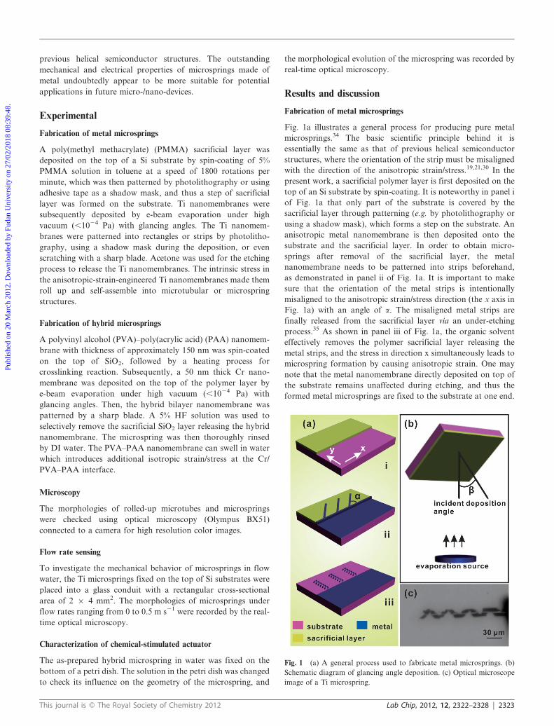
Fig. 1a illustrates a general process for producing pure metal
microsprings.34 The basic scientific principle behind it is
essentially the same as that of previous helical semiconductor
structures, where the orientation of the strip must be misaligned
with the direction of the anisotropic strain/stress.19,21,30 In the
present work, a sacrificial polymer layer is first deposited on the
top of an Si substrate by spin-coating. It is noteworthy in panel i
of Fig. 1a that only part of the substrate is covered by the
sacrificial layer through patterning (e.g. by photolithography or
using a shadow mask), which forms a step on the substrate. An
anisotropic metal nanomembrane is then deposited onto the
substrate and the sacrificial layer. In order to obtain micro-
springs after removal of the sacrificial layer, the metal
nanomembrane needs to be patterned into strips beforehand,
as demonstrated in panel ii of Fig. 1a. It is important to make
sure that the orientation of the metal strips is intentionally
misaligned to the anisotropic strain/stress direction (the x axis in
Fig. 1a) with an angle of a. The misaligned metal strips are
finally released from the sacrificial layer via an under-etching
process.35 As shown in panel iii of Fig. 1a, the organic solvent
effectively removes the polymer sacrificial layer releasing the
metal strips, and the stress in direction x simultaneously leads to
microspring formation by causing anisotropic strain. One may
note that the metal nanomembrane directly deposited on top of
the substrate remains unaffected during etching, and thus the
formed metal microsprings are fixed to the substrate at one end.
Fig. 1 (a) A general process used to fabricate metal microsprings. (b)
Schematic diagram of glancing angle deposition. (c) Optical microscope
image of a Ti microspring.
This journal is � The Royal Society of Chemistry 2012 Lab Chip, 2012, 12, 2322–2328 | 2323
Publ
ishe
d on
20
Mar
ch 2
012.
Dow
nloa
ded
by F
udan
Uni
vers
ity o
n 27
/02/
2018
08:
39:4
8.
View Article Online
We should stress that the fixing of microsprings onto a substrate
is quite useful in the accurate positioning and integration of
microsprings on a single chip, and this is also of benefit to the
applications discussed later.
Obviously, the most important part of the process is to
introduce strain anisotropy in the metal nanomembrane
deposited by evaporation, which was previously considered to
be a serious stumbling block.30 We successfully solve this
problem by engaging glancing angle deposition (GLAD) which
has been used to obtain films consisting of nanopillars/nanorods
with dimensions measuring tens of nanometers due to an atomic
shadowing effect under limited adatom mobility conditions.36,37
Fig. 1b schematically shows the configuration corresponding to
GLAD employed in our work. The sample is fixed on the sample
holder and the normal direction of the sample surface is set to an
angle b with respect to the direction of material flux during
deposition (see Fig. 1b). We have found this approach can
effectively introduce anisotropy into the nanomembrane, and the
strips cut from the nanomembrane deterministically roll up into
microspring structures.34 An optical image of a typical Ti
microspring fabricated using the above approach is shown in
Fig. 1c, which validates the feasibility of our method.
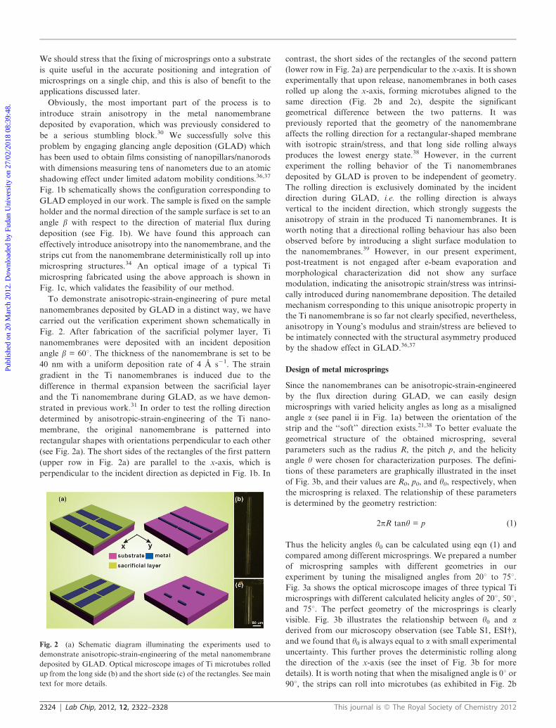
To demonstrate anisotropic-strain-engineering of pure metal
nanomembranes deposited by GLAD in a distinct way, we have
carried out the verification experiment shown schematically in
Fig. 2. After fabrication of the sacrificial polymer layer, Ti
nanomembranes were deposited with an incident deposition
angle b = 60u. The thickness of the nanomembrane is set to be
40 nm with a uniform deposition rate of 4 A s21. The strain
gradient in the Ti nanomembranes is induced due to the
difference in thermal expansion between the sacrificial layer
and the Ti nanomembrane during GLAD, as we have demon-
strated in previous work.31 In order to test the rolling direction
determined by anisotropic-strain-engineering of the Ti nano-
membrane, the original nanomembrane is patterned into
rectangular shapes with orientations perpendicular to each other
(see Fig. 2a). The short sides of the rectangles of the first pattern
(upper row in Fig. 2a) are parallel to the x-axis, which is
perpendicular to the incident direction as depicted in Fig. 1b. In
contrast, the short sides of the rectangles of the second pattern
(lower row in Fig. 2a) are perpendicular to the x-axis. It is shown
experimentally that upon release, nanomembranes in both cases
rolled up along the x-axis, forming microtubes aligned to the
same direction (Fig. 2b and 2c), despite the significant
geometrical difference between the two patterns. It was
previously reported that the geometry of the nanomembrane
affects the rolling direction for a rectangular-shaped membrane
with isotropic strain/stress, and that long side rolling always
produces the lowest energy state.38 However, in the current
experiment the rolling behavior of the Ti nanomembranes
deposited by GLAD is proven to be independent of geometry.
The rolling direction is exclusively dominated by the incident
direction during GLAD, i.e. the rolling direction is always
vertical to the incident direction, which strongly suggests the
anisotropy of strain in the produced Ti nanomembranes. It is
worth noting that a directional rolling behaviour has also been
observed before by introducing a slight surface modulation to
the nanomembranes.39 However, in our present experiment,
post-treatment is not engaged after e-beam evaporation and
morphological characterization did not show any surface
modulation, indicating the anisotropic strain/stress was intrinsi-
cally introduced during nanomembrane deposition. The detailed
mechanism corresponding to this unique anisotropic property in
the Ti nanomembrane is so far not clearly specified, nevertheless,
anisotropy in Young’s modulus and strain/stress are believed to
be intimately connected with the structural asymmetry produced
by the shadow effect in GLAD.36,37
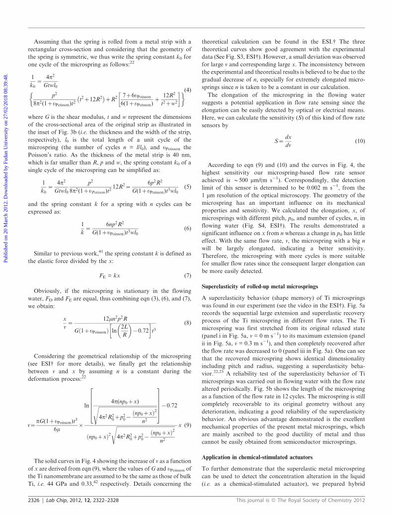
Design of metal microsprings
Since the nanomembranes can be anisotropic-strain-engineered
by the flux direction during GLAD, we can easily design
microsprings with varied helicity angles as long as a misaligned
angle a (see panel ii in Fig. 1a) between the orientation of the
strip and the ‘‘soft’’ direction exists.21,38 To better evaluate the
geometrical structure of the obtained microspring, several
parameters such as the radius R, the pitch p, and the helicity
angle h were chosen for characterization purposes. The defini-
tions of these parameters are graphically illustrated in the inset
of Fig. 3b, and their values are R0, p0, and h0, respectively, when
the microspring is relaxed. The relationship of these parameters
is determined by the geometry restriction:
2pR tanh = p (1)
Thus the helicity angles h0 can be calculated using eqn (1) and
compared among different microsprings. We prepared a number
of microspring samples with different geometries in our
experiment by tuning the misaligned angles from 20u to 75u.Fig. 3a shows the optical microscope images of three typical Ti
microsprings with different calculated helicity angles of 20u, 50u,and 75u. The perfect geometry of the microsprings is clearly
visible. Fig. 3b illustrates the relationship between h0 and a
derived from our microscopy observation (see Table S1, ESI{),
and we found that h0 is always equal to a with small experimental
uncertainty. This further proves the deterministic rolling along
the direction of the x-axis (see the inset of Fig. 3b for more
details). It is worth noting that when the misaligned angle is 0u or
90u, the strips can roll into microtubes (as exhibited in Fig. 2b
Fig. 2 (a) Schematic diagram illuminating the experiments used to
demonstrate anisotropic-strain-engineering of the metal nanomembrane
deposited by GLAD. Optical microscope images of Ti microtubes rolled
up from the long side (b) and the short side (c) of the rectangles. See main
text for more details.
2324 | Lab Chip, 2012, 12, 2322–2328 This journal is � The Royal Society of Chemistry 2012
Publ
ishe
d on
20
Mar
ch 2
012.
Dow
nloa
ded
by F
udan
Uni
vers
ity o
n 27
/02/
2018
08:
39:4
8.
View Article Online

and 2c, or into microrings if the strips are narrow enough) rather
than microsprings. In previous helical semiconductor structures,
the helicity angle is inherently larger than 45u due to equivalent
,100. directions of silicon crystal, and smaller angles could
only be achieved by using a narrow strip or adding an additional
Cr layer.21,30 Such limitations do not exist in the present case
because there is only one preferred rolling direction, i.e. along
the x-axis, which makes it possible to fabricate microsprings of
single materials with h0 in a large range, independent of the strip
width. In addition, our approach of microspring fabrication also
demonstrates good controllability in geometry tuning compared
to previous work.20 For instance, the diameter and the chirality
of the microsprings can be controlled by altering the thickness
and the orientation of the original metal strips (see Fig. S1 and
Fig. S2 for more details, ESI{).
Application in liquid flow rate sensing
The mechanical properties of Ti microsprings in flowing water
were studied using a device illustrated in the inset of Fig. 4, where
the microspring fixed on the substrate is placed in the center of a
glass conduit filled with flowing water. The real-time geometrical
change of the microspring can therefore be observed and recorded
by optical microscopy. The experimental relationships between
the elongation (x) and the flow rate (v) for three different Ti
microsprings with R0 of y10 mm are shown in Fig. 4 using
triangles, squares, and circles, respectively. One can see that the
elongation increases with the flow rate when the elongation is
relatively small, but gradually becomes saturated at large
elongations, where the microsprings have been stretched to shapes
close to their original morphologies i.e. strips. This will be
discussed later to show the superelasticity of the Ti microsprings.
In the following part, we will try to understand the mechanical
properties of the microspring by theoretical calculations based on
its unique geometry. In flowing water, the microspring is subjected
to the drag force (FD), which is balanced by the elastic force (FE).
The drag force applied onto the microspring is rather complicated
and for simplification purposes, we assume that the spring is a part
of circular cylinder. Thus FD is considered to be parallel to the
surface and proportional to the surface area. In the case of a
cylindrical structure, the drag force FD,cylinder is in the form of
FD,cylinder~2pmLv
ln2L
R
� �{0:72
(2)
where m is the viscosity of the fluid, y0.001 Pa s for water in the
present case, and L and R are the length and radius of the
corresponding cylinder, respectively.40 Correspondingly, FD on a
microspring can be expressed as:
FD~FD,cylinder
Sspring
Scylinder
~
2pmLv
ln2L
R
� �{0:72
2664
3775 2lw
2pRL~
2mlw
ln2L
R
� �{0:72
� �R
v
(3)
where Sspring is the surface area of the microspring (two sides),
Scylinder is the side area of the cylinder (one side), and l and w the
length and the width of the original metal strip, respectively.
Fig. 3 (a) Optical microscope images of Ti microsprings with helicity
angles of (i) 20u, (ii) 50u, and (iii) 75u. (b) Helicity angle of the
microspring (h0) as the function of the misaligned angle (a) between
the orientation of the strip and the x-axis. The results corresponding to
the structures shown in (a) are labelled. The inset illustrates the definition
of the parameters of the microspring structure.
Fig. 4 Relationship between the flow rate (v) and the elongation of the
Ti microsprings (x). The triangles, squares, and circles are experimental
results from three different Ti microsprings (SP1: n = 2.0; SP2: n = 3.5;
SP3: n = 4.8) and the solid lines in different colors are from theoretical
calculations fitted to corresponding experimental results. The inset shows
the schematic illustration of the device used to investigate the mechanical
properties of Ti microsprings in flowing water.
This journal is � The Royal Society of Chemistry 2012 Lab Chip, 2012, 12, 2322–2328 | 2325
Publ
ishe
d on
20
Mar
ch 2
012.
Dow
nloa
ded
by F
udan
Uni
vers
ity o
n 27
/02/
2018
08:
39:4
8.
View Article Online
Assuming that the spring is rolled from a metal strip with a
rectangular cross-section and considering that the geometry of
the spring is symmetric, we thus write the spring constant k0 for
one cycle of the microspring as follows:22
1
k0~
4p2
Gtwl0
p2
8p2(1zuPoisson)t2t2z12R2� �
zR2 7z6uPoisson
6(1zuPoisson)z
12R2
t2zw2
� �� (4)
where G is the shear modulus, t and w represent the dimensions
of the cross-sectional area of the original strip as illustrated in
the inset of Fig. 3b (i.e. the thickness and the width of the strip,
respectively), l0 is the total length of a unit cycle of the
microspring (the number of cycles n = l/l0), and uPoisson the
Poisson’s ratio. As the thickness of the metal strip is 40 nm,
which is far smaller than R, p and w, the spring constant k0 of a
single cycle of the microspring can be simplified as:
1
k0~
4p2
Gtwl0
p2
8p2(1zuPoisson)t212R2~
6p2R2
G(1zuPoisson)t3wl0(5)
and the spring constant k for a spring with n cycles can be
expressed as:
1
k~
6np2R2
G(1zuPoisson)t3wl0(6)
Similar to previous work,41 the spring constant k is defined as
the elastic force divided by the x:
FE = kx (7)
Obviously, if the microspring is stationary in the flowing
water, FD and FE are equal, thus combining eqn (3), (6), and (7),
we obtain:
x
v~
12mn2p2R
G 1zuPoissonð Þ ln2L
R
� �{0:72
� �t3
(8)
Considering the geometrical relationship of the microspring
(see ESI{ for more details), we finally get the relationship
between v and x by assuming n is a constant during the
deformation process:22
v~pG(1zuPoisson)t3
6m|
ln4p(np0zx)ffiffiffiffiffiffiffiffiffiffiffiffiffiffiffiffiffiffiffiffiffiffiffiffiffiffiffiffiffiffiffiffiffiffiffiffiffiffiffiffiffiffiffiffiffiffiffi
4p2R20zp2
0{np0zxð Þ2
n2
s
266664
377775{0:72
np0zxð Þ2ffiffiffiffiffiffiffiffiffiffiffiffiffiffiffiffiffiffiffiffiffiffiffiffiffiffiffiffiffiffiffiffiffiffiffiffiffiffiffiffiffiffiffiffiffiffiffi4p2R2
0zp20{
np0zxð Þ2
n2
s x (9)
The solid curves in Fig. 4 showing the increase of v as a function
of x are derived from eqn (9), where the values of G and uPoisson of
the Ti nanomembrane are assumed to be the same as those of bulk
Ti, i.e. 44 GPa and 0.33,42 respectively. Details concerning the
theoretical calculation can be found in the ESI.{ The three
theoretical curves show good agreement with the experimental
data (See Fig. S3, ESI{). However, a small deviation was observed
for large v and corresponding large x. The inconsistency between
the experimental and theoretical results is believed to be due to the
gradual decrease of n, especially for extremely elongated micro-
springs since n is taken to be a constant in our calculation.
The elongation of the microspring in the flowing water
suggests a potential application in flow rate sensing since the
elongation can be easily detected by optical or electrical means.
Here, we can calculate the sensitivity (S) of this kind of flow rate
sensors by
S~dx
dv(10)
According to eqn (9) and (10) and the curves in Fig. 4, the
highest sensitivity our microspring-based flow rate sensor
achieved is y500 mm/(m s21). Correspondingly, the detection
limit of this sensor is determined to be 0.002 m s21, from the
1 mm resolution of the optical microscopy. The geometry of the
microspring has an important influence on its mechanical
properties and sensitivity. We calculated the elongation, x, of
microsprings with different pitch, p0, and number of cycles, n, in
flowing water (Fig. S4, ESI{). The results demonstrated a
significant influence on x from n whereas a change in p0 has little
effect. With the same flow rate, v, the microspring with a big n
will be largely elongated, indicating a better sensitivity.
Therefore, the microspring with more cycles is more suitable
for smaller flow rates since the consequent larger elongation can
be more easily detected.
Superelasticity of rolled-up metal microsprings
A superelasticity behavior (shape memory) of Ti microsprings
was found in our experiment (see the video in the ESI{). Fig. 5a
records the sequential large extension and superelastic recovery
process of the Ti microspring in different flow rates. The Ti
microspring was first stretched from its original relaxed state
(panel i in Fig. 5a, v = 0 m s21) to its maximum extension (panel
ii in Fig. 5a, v = 0.3 m s21), and then completely recovered after
the flow rate was decreased to 0 (panel iii in Fig. 5a). One can see
that the recovered microspring shows identical dimensionality
including pitch and radius, suggesting a superelasticity beha-
vior.22,23 A reliability test of the superelasticity behavior of Ti
microsprings was carried out in flowing water with the flow rate
altered periodically. Fig. 5b shows the length of the microspring
as a function of the flow rate in 12 cycles. The microspring is still
completely recoverable to its original geometry without any
deterioration, indicating a good reliability of the superelasticity
behavior. An obvious advantage demonstrated is the excellent
mechanical properties of the present metal microsprings, which
are mainly ascribed to the good ductility of metal and thus
cannot be easily obtained from semiconductor microsprings.
Application in chemical-stimulated actuators
To further demonstrate that the superelastic metal microspring
can be used to detect the concentration alteration in the liquid
(i.e. as a chemical-stimulated actuator), we prepared hybrid
2326 | Lab Chip, 2012, 12, 2322–2328 This journal is � The Royal Society of Chemistry 2012
Publ
ishe
d on
20
Mar
ch 2
012.
Dow
nloa
ded
by F
udan
Uni
vers
ity o
n 27
/02/
2018
08:
39:4
8.
View Article Online
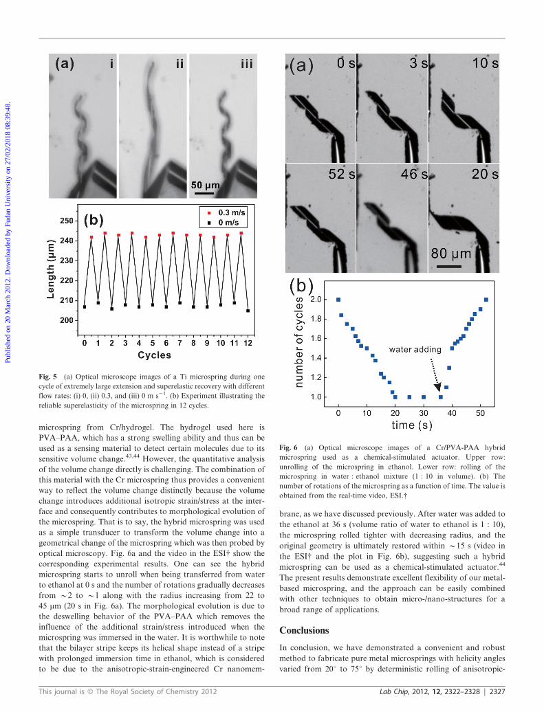
microspring from Cr/hydrogel. The hydrogel used here is
PVA–PAA, which has a strong swelling ability and thus can be
used as a sensing material to detect certain molecules due to its
sensitive volume change.43,44 However, the quantitative analysis
of the volume change directly is challenging. The combination of
this material with the Cr microspring thus provides a convenient
way to reflect the volume change distinctly because the volume
change introduces additional isotropic strain/stress at the inter-
face and consequently contributes to morphological evolution of
the microspring. That is to say, the hybrid microspring was used
as a simple transducer to transform the volume change into a
geometrical change of the microspring which was then probed by
optical microscopy. Fig. 6a and the video in the ESI{ show the
corresponding experimental results. One can see the hybrid
microspring starts to unroll when being transferred from water
to ethanol at 0 s and the number of rotations gradually decreases
from y2 to y1 along with the radius increasing from 22 to
45 mm (20 s in Fig. 6a). The morphological evolution is due to
the deswelling behavior of the PVA–PAA which removes the
influence of the additional strain/stress introduced when the
microspring was immersed in the water. It is worthwhile to note
that the bilayer stripe keeps its helical shape instead of a stripe
with prolonged immersion time in ethanol, which is considered
to be due to the anisotropic-strain-engineered Cr nanomem-
brane, as we have discussed previously. After water was added to
the ethanol at 36 s (volume ratio of water to ethanol is 1 : 10),
the microspring rolled tighter with decreasing radius, and the
original geometry is ultimately restored within y15 s (video in
the ESI{ and the plot in Fig. 6b), suggesting such a hybrid
microspring can be used as a chemical-stimulated actuator.44
The present results demonstrate excellent flexibility of our metal-
based microspring, and the approach can be easily combined
with other techniques to obtain micro-/nano-structures for a
broad range of applications.
Conclusions
In conclusion, we have demonstrated a convenient and robust
method to fabricate pure metal microsprings with helicity angles
varied from 20u to 75u by deterministic rolling of anisotropic-
Fig. 6 (a) Optical microscope images of a Cr/PVA-PAA hybrid
microspring used as a chemical-stimulated actuator. Upper row:
unrolling of the microspring in ethanol. Lower row: rolling of the
microspring in water : ethanol mixture (1 : 10 in volume). (b) The
number of rotations of the microspring as a function of time. The value is
obtained from the real-time video, ESI.{
Fig. 5 (a) Optical microscope images of a Ti microspring during one
cycle of extremely large extension and superelastic recovery with different
flow rates: (i) 0, (ii) 0.3, and (iii) 0 m s21. (b) Experiment illustrating the
reliable superelasticity of the microspring in 12 cycles.
This journal is � The Royal Society of Chemistry 2012 Lab Chip, 2012, 12, 2322–2328 | 2327
Publ
ishe
d on
20
Mar
ch 2
012.
Dow
nloa
ded
by F
udan
Uni
vers
ity o
n 27
/02/
2018
08:
39:4
8.
View Article Online
strain-engineered nanomembranes prepared by GLAD. The
microsprings are found to stretch in flowing water due to the
drag force, and the elongation as a function of flow rate is
observed experimentally and can be well predicted by theoretical
calculations, indicating potential applications of the metal
microsprings in flow rate sensing. The superelasticity behavior
of Ti microsprings and the corresponding reliability was
demonstrated after more than 10 cycles of extremely large
extension and superelastic recovery (shape memory). We further
disclosed the water–ethanol chemical-stimulated actuators appli-
cation of the Cr/PVA–PAA microspring. The excellent mechan-
ical and electric properties of metal itself, as well as the
superelastic property, suggest a great number of potential
applications for metal microsprings in micro-/nano-electrome-
chanical systems.45
Acknowledgements
This work is supported by the Natural Science Foundation of
China (Nos. 61008029, 51102049, 51103027, and 11104040),
Program for New Century Excellent Talents in University (No.
NCET-10-0345), and ‘‘Shu Guang’’ project by Shanghai
Municipal Education Commission and Shanghai Education
Development Foundation. YFM also thanks the support from
the Visiting Scholar Foundation of Key Laboratory of Opto-
electronic Technology and Systems in Chongqing University.
References
1 J. A. Rogers, M. G. Lagally and R. G. Nuzzo, Nature, 2011, 477, 45.2 Y. F. Mei, A. A. Solovev, S. Sanchez and O. G. Schmidt, Chem. Soc.
Rev., 2011, 40, 2109.3 A. Cho, Science, 2006, 313, 164.4 H. J. Jeon, Y. K. Baek, S. B. Yang, S. K. Lee, J. M. Jung and H. T.
Jung, J. Mater. Chem., 2011, 21, 14285.5 Y. F. Hu, Y. Zhang, C. Xu, G. Zhu and Z. L. Wang, Nano Lett.,
2010, 10, 5025.6 M. H. Huang, C. Boone, M. Roberts, D. E. Savage, M. G. Lagally, N.
Shaji, H. Qin, R. Blick, J. A. Nairn and F. Liu, Adv. Mater., 2005, 17, 2860.7 I. S. Chun, V. B. Verma, V. C. Elarde, S. W. Kim, J. M. Zuo, J. J.
Coleman and X. Li, J. Cryst. Growth, 2008, 310, 2353.8 A. A. Solovev, S. Sanchez, M. Pumera, Y. F. Mei and O. G. Schmidt,
Adv. Funct. Mater., 2010, 20, 2430.9 Q. Yang, X. Guo, W. Wang, Y. Zhang, S. Xu, S. H. Lien and Z. L.
Wang, ACS Nano, 2010, 4, 6285–6291.10 R. Attia, D. C. Pregibon, P. S. Doyle, J.-L. Viovy and D. Bartolo,
Lab Chip, 2009, 9, 1213.11 S. Mendach, R. Songmuang, S. Kiravittaya, A. Rastelli, M.
Benyoucef and O. G. Schmidt, Appl. Phys. Lett., 2006, 88, 111120.12 A. Ghosh and P. Fischer, Nano Lett., 2009, 9, 2243.13 A. J. Hong, C. C. Liu, Y. Wang, J. Kim, F. Xiu, S. Ji, J. Zou, P. F.
Nealey and K. L. Wang, Nano Lett., 2010, 10, 224.
14 L. Liu, S. H. Yoo, S. A. Lee and S. Park, Nano Lett., 2011, 11, 3979.15 J. K. Gansel, M. Thiel, M. S. Rill, M. Decker, K. Bade, V. Saile, G.
von Freymann, S. Linden and M. Wegener, Science, 2009, 325, 1513.16 E. J. Smith, D. Makarov, S. Sanchez, V. M. Fomin and O. G.
Schmidt, Phys. Rev. Lett., 2011, 107, 097204.17 D. J. Bell, Y. Sun, L. Zhang, L. X. Dong, B. J. Nelson and D.
Grutzmacher, Sens. Actuators, A, 2006, 130, 54.18 L. Zhang, K. E. Peyer and B. J. Nelson, Lab Chip, 2010, 10, 2203.19 D. J. Bell, L. Dong, B. J. Nelson, M. Golling, L. Zhang and D.
Grutzmacher, Nano Lett., 2006, 6, 725.20 E. J. Smith, D. Makarov and O. G. Schmidt, Soft Matter, 2011, 7,
11309.21 L. Zhang, E. Deckhardt, A. Weber, C. Schonenberger and D.
Grutzmacher, Nanotechnology, 2005, 16, 655.22 P. X. Gao, W. Mai and Z. L. Wang, Nano Lett., 2006, 6, 2536.23 C. Cao, H. Du, Y. Xu, H. Zhu, T. Zhang and R. Yang, Adv. Mater.,
2008, 20, 1738.24 K. W. Park, Y. E. Sung, S. Han, Y. Yun and T. Hyeon, J. Phys.
Chem. B, 2004, 108, 939.25 H. F. Zhang, C. M. Wang, E. C. Buck and L. S. Wang, Nano Lett.,
2003, 3, 577.26 X. Y. Kong, Y. Ding, R. Yang and Z. L. Wang, Science, 2004, 303,
1348.27 I. S. Chun, K. Bassett, A. Challa and X. Li, Appl. Phys. Lett., 2010,
96, 251106.28 V. Y. Prinz, V. A. Seleznev, A. K. Gutakovsky, A. V. Chehovskiy,
V. V. Preobrazhenskii, M. A. Putyato and T. A. Gavrilova, Phys. E.,2000, 6, 828.
29 O. G. Schmidt and K. Eberl, Nature, 2001, 410, 168.30 L. Zhang, E. Ruh, D. Grutzmacher, L. X. Dong, D. J. Bell, B. J.
Nelson and C. Schonenberger, Nano Lett., 2006, 6, 1311.31 Y. F. Mei, G. S. Huang, A. A. Solovev, E. Bermudez-Urena, I.
Monch, F. Ding, T. Reindl, R. K. Y. Fu, P. K. Chu and O. G.Schmidt, Adv. Mater., 2008, 20, 4085.
32 L. Zhang, R. Tu and H. Dai, Nano Lett., 2006, 6, 2785.33 S. Heiroth, R. Ghisleni, T. Lippert, J. Michler and A. Wokaun, Acta
Mater., 2011, 59, 2330.34 W. M. Li, G. S. Huang, X. J. Wu and Y. F. Mei, CN patent
application, 2011, 201110262186.4.35 G. S. Huang, Y. F. Mei, D. J. Thurmer, E. Coric and O. G. Schmidt,
Lab Chip, 2009, 9, 263.36 K. Robbie, M. J. Brett and A. Lakhtakia, Nature, 1996, 384, 616.37 S. V. Kesapragada, P. Victor, O. Nalamasu and D. Gall, Nano Lett.,
2006, 6, 854.38 I. S. Chun, A. Challa, B. Derickson, K. J. Hsia and X. Li, Nano Lett.,
2010, 10, 3927.39 P. Cendula, S. Kiravittaya, I. Monch, J. Schumann and O. G.
Schmidt, Nano Lett., 2011, 11, 236.40 J. Happle and H. Brenner, Low Reynolds Number Hydrodynamics,
Prentice Hall: Englewood Cliffs, NJ, USA, 1965.41 X. Chen, S. Zhang, D. A. Dikin, W. Ding, R. S. Ruoff, L. Pan and Y.
Nakayama, Nano Lett., 2003, 3, 1299.42 C. Leyens and M. Peters, Titanium and titanium alloys: fundamentals
and applications, Wiley-VCH, Weinheim, Germany, 2003.43 J. Sorber, G. Steiner, V. Schulz, M. Guenther, G. Gerlach, R. Salzer
and K. F. Arndt, Anal. Chem., 2008, 80, 2957.44 G. Gerlach, M. Guenther, J. Sorber, G. Suchaneck, K. F. Arndt and
A. Richter, Sens. Actuators, B, 2005, 111, 555.45 Feng Liu, M. G. Lagally and J. Zang, MRS Bull., 2009, 34, 190.
2328 | Lab Chip, 2012, 12, 2322–2328 This journal is � The Royal Society of Chemistry 2012
Publ
ishe
d on
20
Mar
ch 2
012.
Dow
nloa
ded
by F
udan
Uni
vers
ity o
n 27
/02/
2018
08:
39:4
8.
View Article Online