Embed Size (px)
Citation preview
Digital Circuit Lab
Lab 7: Matrix Multiplication Circuit for Real
Chun-Jen Tsai and Lan-Da Van
Department of Computer Science
National Chiao Tung University
Taiwan, R.O.C.
Fall, 2019

Lab 7
Digital Circuit Lab
Lab 7: Matrix Multiplication
In this lab, you will design a circuit to do 44 matrix
multiplications.
Your circuit has an Block RAM (BRAM) that stores two 44
matrices.
The user press BTN1 to start the circuit
The circuit reads the matrices, perform the multiplication,
and print the output matrix through the UART to a terminal
window
The lab file submission deadline is on 11/25 by
6:00pm.
2

Lab 7
Digital Circuit Lab
Design Constraint of Lab 7
You must use no more than 16 multipliers to
implement your circuit
Each Atrix-7 35T FPGA on the Arty board has 90 2018-bit
multipliers
Your grade will be based on correctness and logic
usage; the smaller the logic, the better
The “size” of the logic is calculated by the number of
physical multipliers, LUTs, Flip-flops (FFs)
BRAM blocks are considered as memory resource, not logic
resource
3
Lab 7
Digital Circuit Lab
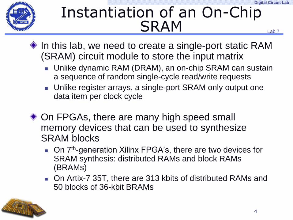
Instantiation of an On-Chip SRAM
In this lab, we need to create a single-port static RAM (SRAM) circuit module to store the input matrix Unlike dynamic RAM (DRAM), an on-chip SRAM can sustain
a sequence of random single-cycle read/write requests
Unlike register arrays, a single-port SRAM only output one data item per clock cycle
On FPGAs, there are many high speed small memory devices that can be used to synthesize SRAM blocks On 7th-generation Xilinx FPGA’s, there are two devices for
SRAM synthesis: distributed RAMs and block RAMs (BRAMs)
On Artix-7 35T, there are 313 kbits of distributed RAMs and 50 blocks of 36-kbit BRAMs
4

Lab 7
Digital Circuit Lab
SRAM on FPGAs
In Verilog, we can instantiate an SRAM module using
explicit declaration† or implicit inferencing
For example, a single-port SRAM can be instantiated using
the module BRAM_SINGLE_MACRO in Vivado
5† Xilinx UG953, Vivado Design Suite 7 Series FPGA and Zynq-7000 All Programmable SoC Libraries Guide, page 120.

Lab 7
Digital Circuit Lab
General SRAM Signals (1/2)
CLK – Clock
Independent clock pins for synchronous operations
EN – Enable
The read, write and reset functionality of the port is only
active when this signal is enabled
WE – Write enable
When active, the contents of the data input bus are written to
the RAM, and the new data also reflects on the data out bus
When inactive, a read operation occurs and the contents of
the memory cells reflect on the data out bus
ADDR – Address
The address bus selects the memory cells for read or write
6
Lab 7
Digital Circuit Lab
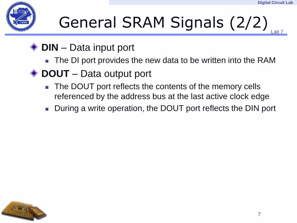
General SRAM Signals (2/2)
DIN – Data input port
The DI port provides the new data to be written into the RAM
DOUT – Data output port
The DOUT port reflects the contents of the memory cells
referenced by the address bus at the last active clock edge
During a write operation, the DOUT port reflects the DIN port
7
Lab 7
Digital Circuit Lab
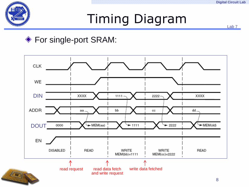
Timing Diagram
For single-port SRAM:
8
DIN
DOUT
read request read data fetchand write request
write data fetched

Lab 7
Digital Circuit Lab
Instantiate an SRAM by Inference
The following Verilog code infers an SRAM block:
The allocation unit size of SRAM on Artix-7s is 18-kbit
(If you allocate an 8-kbit memory, it will still use an 18-kbit
memory block to synthesize it.)
9
reg [7:0] sram[511:0];wire sram_we, sram_en;reg [7:0] data_out;wire [7:0] data_in;wire [8:0] sram_addr;
always @(posedge clk) begin // Write data into the SRAM blockif (sram_en && sram_we) beginsram[sram_addr] <= data_in;
endend
always @(posedge clk) begin // Read data from the SRAM blockif (sram_en && sram_we) // If data is being written into SRAM,data_out <= data_in; // forward the data to the read port
elsedata_out <= sram[sram_addr]; // Send data to the read port
end

Lab 7
Digital Circuit Lab
The Sample Code of Lab 7 (1/2)
The sample code of lab 7 shows you how to create a
SRAM block in FPGA with some data pre-stored in it
The data for the two matrices are pre-stored in SRAM
Initialization of an SRAM block can be done as follows:
10
// This is a code segment from the sram module.
// Declareation of the memory cells
reg [DATA_WIDTH-1 : 0] RAM [RAM_SIZE - 1:0];
// ------------------------------------
// SRAM cell initialization
// ------------------------------------
initial begin
$readmemh(“matrices.mem", RAM);
end
E1
6B
D7
1D
B6
0C
55
2D
$readmemh() is only synthesizable for FPGAs.
You cannot use this for ASIC design!
The content of “matrices.mem”
8 bits

Lab 7
Digital Circuit Lab
The Sample Code of Lab 7 (2/2)
The memory is added to the project as a design source:
11

Lab 7
Digital Circuit Lab
Input Matrix Format (MEM File)
Each input matrix has 16 unsigned 8-bit elements of
values between 0 ~ 255 in the column-major format
The staring address of the first matrix in the on-chip
SRAM memory is at 0x0000, and the second matrix
is at 0x0010
The output matrix has 16 unsigned 18-bit elements
12

Lab 7
Digital Circuit Lab
Demo of the Lab 7 Sample System
Once you configured the FPGA, you will see the
content of the SRAM on the LCD screen
Use BTN0/BTN1 to browse through the SRAM cells
13

Lab 7
Digital Circuit Lab
Things to do in Lab 7
For Lab 7, after the multiplication, your circuit must
print the resulting matrix to the UART as follows:
14
The matrix multiplication result
is:
[ 11CE9, 18749, 0EE26, 16F64 ]
[ 0ED5B, 1091D, 04768, 06376 ]
[ 167B9, 1BF8A, 0E496, 1504F ]
[ 09901, 0F404, 08F23, 0C4A5 ]

Lab 7
Digital Circuit Lab
Connecting SRAM to Datapath
Since a single-port 8-bit SRAM only output one data
per clock cycle, you cannot connect an SRAM
directly to a parallel-input matrix multiplication
datapath
Two possible solutions:
Use multiple SRAM blocks, each block has one or two
address/data ports
In the FSM, design a state to sequentially read the data from
the SRAM, and store them in register arrays for parallel
computation later
15

Lab 7
Digital Circuit Lab
Timing Issues on Long Combinational Path
A long arithmetic equation will be synthesized into a
multi-level combinational circuit path:
16
reg [15:0] a[0:15];
reg [15:0] b[0:15];
reg [31:0] c[0:15];
always @(posedge clk)
case (j)
0: c[i*4] <=
a[i*4+0]*b[0*4] +
a[i*4+1]*b[1*4] +
a[i*4+2]*b[2*4] +
a[i*4+3]*b[3*4];
1: . . .
2: . . .
3: . . .
endcase
b0j
b1j
b3j
+
+
012
3
01
23
012
3
012
3
b2j
+
cij
ja00
a10
a20
a30
a01
a11
a21
a31
a03
a13
a23
a33
a02
a12
a22
a32
Delay must be less than one cycle!

Lab 7
Digital Circuit Lab
Setup Time and Hold Time
To store values into flip-flops (registers) properly, the
minimum allowable clock period Tmin is computed by
Tmin = Tpath_delay + Tsetup
Tpath_delay is the propagation delay through logics and wires
Tsetup is the minimum time data must arrive at D before
the next rising edge of clock (setup time)
17
Lab 7
Digital Circuit Lab
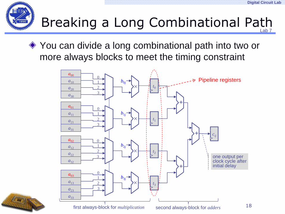
Breaking a Long Combinational Path
You can divide a long combinational path into two or
more always blocks to meet the timing constraint
18
a00
a10
a20
a30
a01
a11
a21
a31
a03
a13
a23
a33
b0j
b1j
b3j
+
+
0
1
2
3
0
1
2
3
0
1
2
3
a02
a12
a22
a32
0
1
2
3
b2j
+
one output per clock cycle afterinitial delay
t0
t1
t2
t3
Pipeline registers
cij
first always-block for multiplication second always-block for adders

Lab 7
Digital Circuit Lab
Check FPGA Resource Utilization
19
Used 0.5 block of a 36-kbit BRAM.