Embed Size (px)
Citation preview

1
Lab 3 Layout Using Virtuoso Layout
XL (VXL)
This Lab will go over:
1. Creating layout with Virtuoso layout XL (VXL).
2. Transistor Chaining.
3. Creating Standard cell.
4. Manual Routing
5. Providing Substrate or Bulk Connection.
1. Creating layout with Virtuoso layout XL (VXL)
We will be using PCELLs developed by NCSU to layout a 2 inputs nand gate, denoted as nand2.
If you are not running CDS tools, do so according to Lab 1.
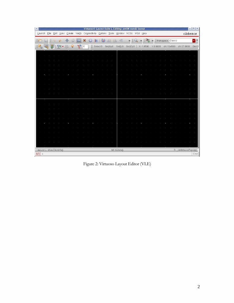
First we need to create a layout view of our nand2. Go to the library manager and execute (LM)File>New>Cell View…. A pop-up like Figure 1 should appear. Fill out the pop-up exactly as in Figure 1, then click OK. The Virtuoso layout editor (VLE) will open as shown in Figure 2.
Figure 1: Creating layout view of nand2
2
Figure 2: Virtuoso Layout Editor (VLE)
3
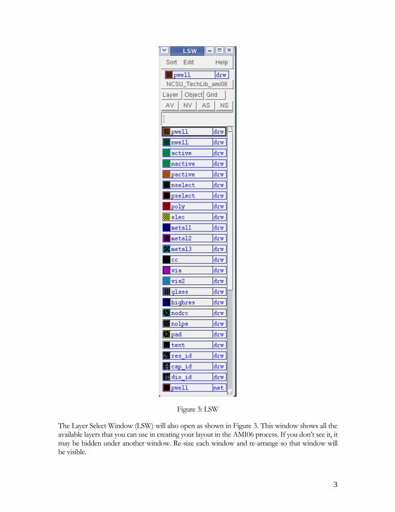
Figure 3: LSW
The Layer Select Window (LSW) will also open as shown in Figure 3. This window shows all the available layers that you can use in creating your layout in the AMI06 process. If you don’t see it, it may be hidden under another window. Re-size each window and re-arrange so that window will be visible.

4
To make sure that all layers will appear in LSW, execute (VLE) Options>Display…. A pop-up will display as in Figure 4, make sure in the Array Display area that the Full radio button is selected. Note that X snap spacing and Y snap spacing should indicate ½ lambda (½* 0.3)=.15 for AMI06 process. Set the pop-up according to Figure 4 and click OK.
Figure 4: Setting Display Options
We will be using the Virtuoso Layout XL (VXL), to help us in creating the layout. This is a schematic driven layout. To invoke VXL, in the layout editor execute (VLE) Launch>LayoutXL. A schematic window showing nand2 schematic will display as shown in Figure 5.

5
Figure 5: Nand2 schematic
To put the components shown in the schematic window into the layout editor, execute (VXL) connectivity>Generate> All from Schematic…. A pop-up will display as in Figure 6. Note all signal I/O pins must be on metal2 layer, power rails (mygnd and myvdd) must be on metal1 layer, and default layer on metal2. In addition, the Create button for mygnd and myvdd must be de-selected. This means that we will do our own placement of mygnd and myvdd. Metal2 is needed for signal I/O pins, to enable the downstream automatic layout generator to successfully layout of a 2-input exclusive or gate (xor2), which consists of inverters and nand2 gates to be discussed in lab 5. Complete the pop-up exactly as shown in Figure 6, then click OK.

6
Figure 6: Display Pin Name Option pop-up

7
The initial component and pin placement is displayed in Figure 7. The components and pins are shown outside a bounding box. This bounding box is an estimate of the optimum size of the final layout. Automatic router to be discussed in Lab 5 will use the bounding box to constraint all routing to occur within the box. The bounding box may need to be re-sized to satisfy our goal of creating standard cells. Standard cells are cells that are created to have the same height, so that when abutting two standard cells both power rails will connect.
Figure 7: Initial component and pin placement

8
Place the component and pin within the bounding box in their relative position as in the schematic, execute. For that execute the (VXL) connectivity->Generate->Place as in Schematic. Figure 8 shows the resulting placement within the bounding box. The bounding box size was estimated based on 4 individual transistors. In this lab, we will introduce transistor chaining, a process of combining two transistors of the same type to share a common substrate. Figure 8 shows the components in level 0 (outline only). To display all levels, press (Shift) f key. To go back to level 0, press (Ctrl) f key.

9
Figure 8: Component and pin placement within the bounding box
2. Transistor Chaining
Figure 9 shows the two pmos transistors with all layers prior to chaining. To determine how chaining should be done, we must first determine how the transistors are interconnected. This is achieved by selecting a transistor (by clicking on it), then put and click the cursor on the selected transistor until the cursor change to four arrow icon, move the transistor. As you move the transistor, “flight line” in bright yellow will appear indicating its interconnection. For chaining the two parallel pmos transistors, we want to combine the drain of transistor M0 and M1 as shown in the schematic. The drain of M0 and M1 are both connected to output pin Y. Most likely the initial transistor configuration will be as follows: M1=|S1|G1|D1| and M0=|S0|G0|D0|. In chaining we like to combine D1 and D0. To achieve this, we need to flip transistor M0, so that its new configuration becomes M0=|D0|G0|S0|. So that after transistor chaining, the combine transistor configuration of M1M0 is |S1|G1|D1/ D0 |G0|S0. To flip transistor M0, first select M0 then execute (VXL)Edit>Move…. A move pop-up will open with three buttons: Rotate (Rotate 90 CCW), Sideways (Flip horizontally), and Upside Down (Flip Vertivally). Select Sideways to flip horizontally. Figure 10 shows the result of flipping M0 and chaining M0 and M1. The chaining is achieved by aligning the contacts. To make sure that the chaining process is properly done perform a DRC check by executing (VXL)Verify>DRC…. A pop-up will display, accept the default setting by clicking OK. Check the CIW window for no error message. If there are errors, they will be highlighted in the VXL window. Correct them before proceeding.

10
Figure 9: The two parallel pmos cells prior to chaining

11
Figure 10: Two pmos cells after chaining

12
Similarly chain the two series connected nmos transistors, M3 and M2. In the schematic, it shows that we need to combine or chain the source of M3 (S3) and the drain of M2(D2). The initial transistor configuration is most likely will be M2=|S2|G2|D2|and M3=|S3|G3|D3|. The desired final configuration of the combined transistor M2M3 is |S2|G2|D2/ S3|G3|D3|. That is, no transistor flipping is required, but must make sure that M3 is to the right of M2. Figure 11 shows the results of chaining the transistors and approximate placement of pins.
2. Creating Standard Cell
Figure 11 also shows the placement of power rails mygnd, myvdd, and nwell. To aid in the creation of standard cells, the placement of power rails should always be in the same height. This is achieved by a macro name “pr”. This macro is executed in the CIW window by typing pr in the CIW command line. The created power rail pins can be verified. Click on the upper metal1, to verify that it corresponds to myvdd pin, as display on the CIW window. Similarly, the lower metal1 corresponds to mygnd pin. The bounding box is re-sized to match the height of the power rails, by executing (VXL)Edit>Stretch, click once on the top edge of the bounding box, the edge will be highlighted, move the edge to match the top of the power rail myvdd, then click once to end the stretch operation. Similarly, move the right edge of the bonding box to match the right edge of the power rails. The macro “pr” was created with nand2 cell layout in mind. In other standard cell layout (say inverter), the right edge of the power rails may need to be moved also. Figure 11 shows a ruler drawn to the left off the bounding box. The ruler is created by executing (VXL) Tools>Create Ruler. Click once on the horizontal axis, and then move vertically toward the top edge of the bounding box. The unit of ruler is in micron (u). Place the pins (B, A, Y) at about 15u. The ruler marker is not part of the layout and is not saved when saving the layout. The marker can be cleared by executing (VXL) Tools>Clear Ruler.

13
Figure 11: Power rails placement and re-sizing of bounding box
14
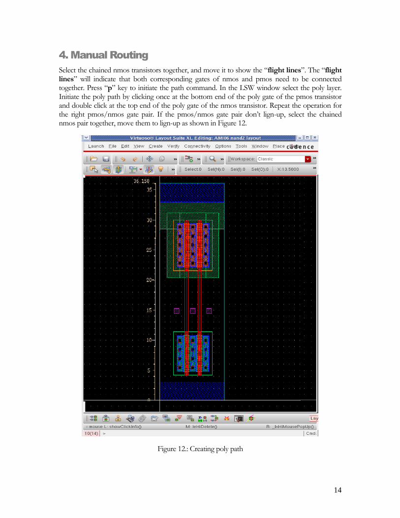
4. Manual Routing
Select the chained nmos transistors together, and move it to show the “flight lines”. The “flight lines” will indicate that both corresponding gates of nmos and pmos need to be connected together. Press “p” key to initiate the path command. In the LSW window select the poly layer. Initiate the poly path by clicking once at the bottom end of the poly gate of the pmos transistor and double click at the top end of the poly gate of the nmos transistor. Repeat the operation for the right pmos/nmos gate pair. If the pmos/nmos gate pair don’t lign-up, select the chained nmos pair together, move them to lign-up as shown in Figure 12.
Figure 12.: Creating poly path

15
To connect the input pin (on metal2 layer) to the gate (on poly layer), we need to establish a common layer to provide the connection. The poly layer can connect to metal1 layer by creating a m1_poly contact, and metal2 layer can connect to metal1 layer by creating a m2_m1 contact (via). Then the two contacts can be connected using metal1 path. Create the m1_poly contact by executing (VXL)Create>via. A pop-up will display, in contact type select M1_POLY as shown in Figure 13.
Figure 13: Creating metal1 to poly contact.
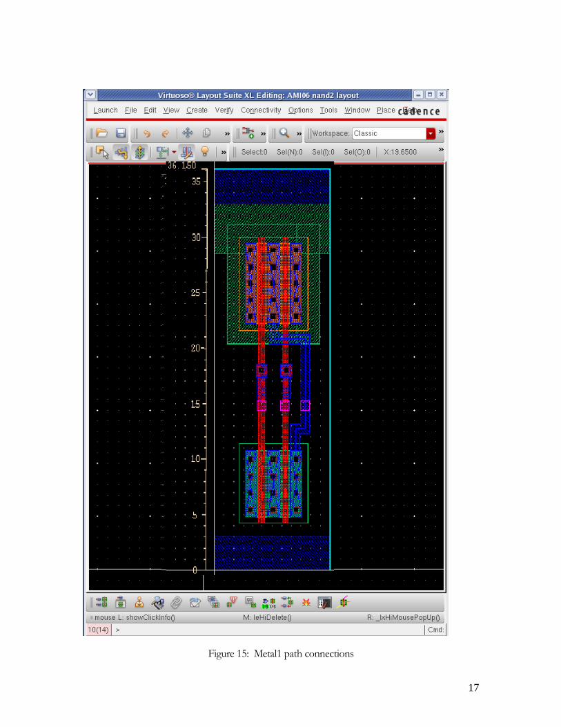
Place the two contacts at around 18u as shown in Figure 14. This figure also shows that each pin has been moved right on top of each corresponding poly gate layer. Create metal1 path by pressing “p” key and selecting metal1 in LSW. To start the metal1 path, click once on the m1_poly contact and double click on the M2 pin. Note each pin will be covered by M2_M1 contact (via) to complete the connection. Repeat for the other m1_poly contact and M2 pin. For the output pin Y connection, it has to be connected to the drain of the chained pmos transistor pair (at the middle) and the drain of the chained nmos transistor pair ( at the right). Create the metal1 path, and connect the path for pin Y as shown in Figure 15.

16
Figure 14: Creating m1_poly contacts
17
Figure 15: Metal1 path connections
18
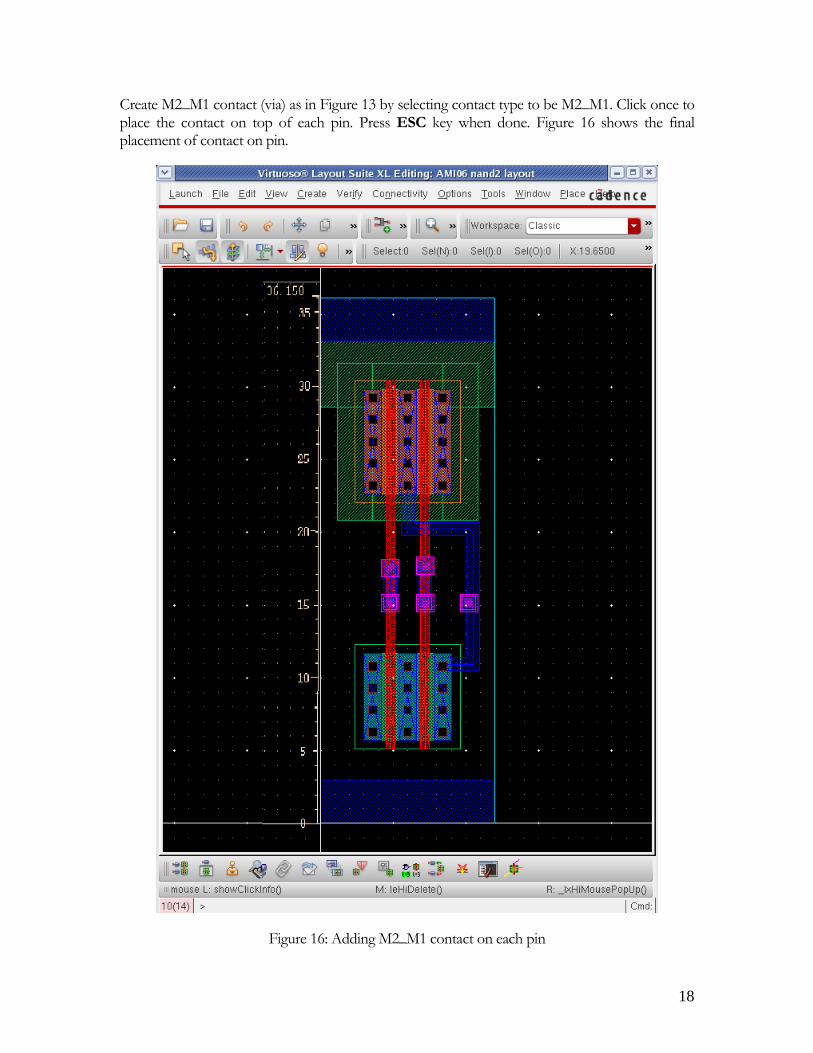
Create M2_M1 contact (via) as in Figure 13 by selecting contact type to be M2_M1. Click once to place the contact on top of each pin. Press ESC key when done. Figure 16 shows the final placement of contact on pin.
Figure 16: Adding M2_M1 contact on each pin

19
5. Providing Substrate or Bulk Connection
To provide a low ohmic contact to the nwell substrate, where pmos transistor resides, NCSU has provided ntap to achieve this. Press “i” to enter the add instance mode. A pop-up appears as in Figure 17. Click Browse and select the NCSU_TechLib_ami06 library, then select ntap in the cell column. Stamp the ntap between the myvdd and nwell, place two-ntap as shown in Figure 18.
Figure 17. Retrieving ntap

20
Figure 18. Stamping ntap
Similarly, retrieve ptap from the NCSU_TechLib_ami06 to provide low ohmic contact to the pwell substrate. In the ami06 technology, the pwell is not drawn because the entire area is assumed to be the pwell substrate. Stamp the ptap between mygnd and pwell substrate (not drawn), place two-ptap as shown in Figure 19.

21
Figure 19. Stamping ptap
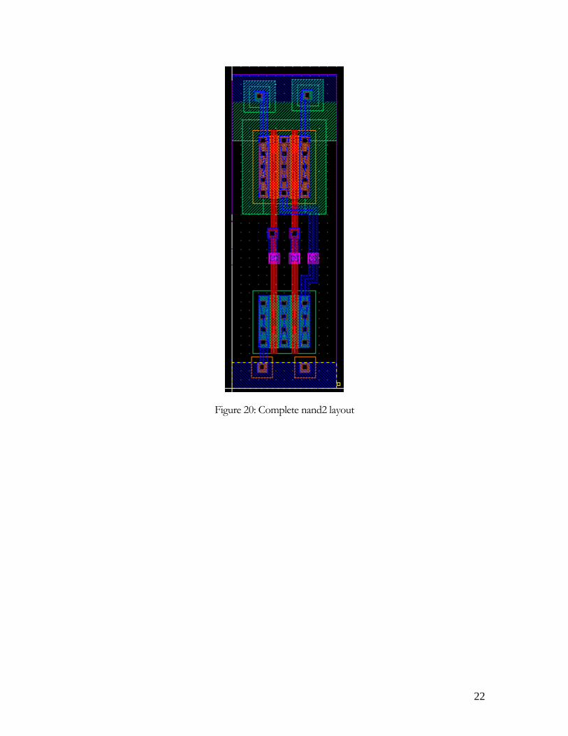
There are three remaining connections. The two sources of the pmos chained pair (M0,M1) need to be connected to myvdd. The source of transistor M2 needs to be connected to mygnd. Figure 20 shows the completed nand2 layout.
22
Figure 20: Complete nand2 layout

23
Assignment:
Create the layout of the inverter (inv) as in Figure 21.
Figure 21: Completed Inv Layout

24