Embed Size (px)
Citation preview

For Academic Use Only
This material exempt per Department of Commerce license exception TSU
Lab 3: Adding Custom IP to an
Embedded System Lab
Targeting MicroBlaze™ on Spartan™-3E Starter Kit

Adding Custom IP Lab: www.xilinx.com/university 3-1 MicroBlaze Processor [email protected]
Lab 3: Adding Custom IP to an Embedded System
Introduction
This lab guides you through the process of adding a custom peripheral to a processor system by
using the Create and Import Peripheral Wizard.
Objectives
After completing this lab, you will be able to:
• Create a custom peripheral
• Add the custom peripheral to your design
• Add pin location constraints
• Generate the bitstream and verify operation in hardware
Procedure
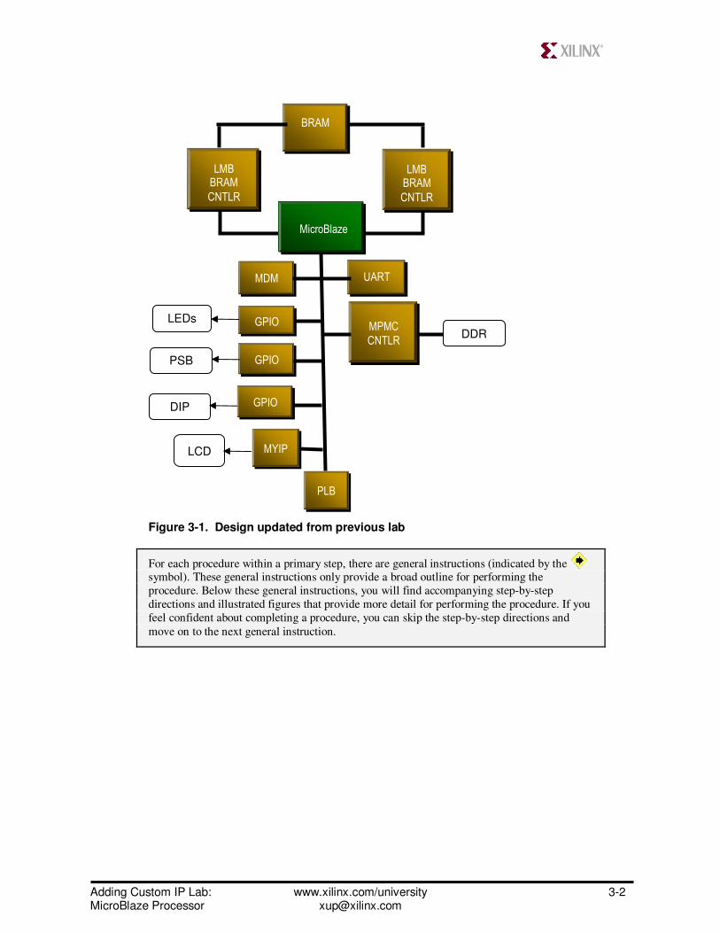
You will extend the Lab 2 hardware design by creating and adding a PLB peripheral (refer to
MYIP in Figure 3-1) to the system, and connecting it to the LCD on the Spartan-3E kit. You
will use the Create and Import Peripheral Wizard of Xilinx Platform Studio (XPS) to generate
the peripheral templates. You will complete the peripheral by adding LCD interface logic in the templates. Next, you will connect the peripheral to the system and add pin location constraints
to connect the LCD controller peripheral to the on-board LCD. Finally, you will verify
operation in hardware using the provided software application.
This lab comprises the following steps:
1. Open the project
2. Generate a peripheral template
3. Create a peripheral
4. Add and connect the peripheral
5. Verify the design in hardware
Adding Custom IP Lab: www.xilinx.com/university 3-2 MicroBlaze Processor [email protected]
Figure 3-1. Design updated from previous lab
For each procedure within a primary step, there are general instructions (indicated by the symbol). These general instructions only provide a broad outline for performing the
procedure. Below these general instructions, you will find accompanying step-by-step
directions and illustrated figures that provide more detail for performing the procedure. If you
feel confident about completing a procedure, you can skip the step-by-step directions and
move on to the next general instruction.
LMB
BRAM
CNTLR
LMB
BRAM
CNTLR
BRAM
PLB
MDM UART
MicroBlaze
GPIO
GPIO
PSB
LEDs
LCD MYIP
GPIO DIP
MPMC
CNTLR DDR

Adding Custom IP Lab: www.xilinx.com/university 3-3 MicroBlaze Processor [email protected]
Opening the Project Step 1
Create a lab3 folder and copy the contents of the lab2 folder into the lab3 folder
if you wish to continue with the design you created in the previous lab,
otherwise copy the lab2 folder content from the labsolution folder into the lab3
folder. Open the project in XPS.
� If you wish to continue using the design that you created in Lab 2, create a lab3 folder in the c:\xup\embedded\labs directory and copy the contents from lab2 to lab3, otherwise
copy the content of lab2 folder from the labsolution folder
� Open XPS by clicking Start →→→→ All Programs →→→→ Xilinx ISE Design Suite 12 →→→→ EDK →→→→
Xilinx Platform Studio
� Select Open a recent project, Click OK and browse to C:\xup\embedded\labs\lab3
� Click system.xmp to open the project
Generate a Peripheral Template Step 2
You will use the Create/Import Peripheral Wizard to create a PLB bus
peripheral template.
� In XPS, select Hardware → Create or Import Peripheral to start the wizard
� Click Next to continue to the Create and Import Peripheral Wizard flow selection (Figure
3-2).

Adding Custom IP Lab: www.xilinx.com/university 3-4 MicroBlaze Processor [email protected]
Figure 3-2. Create and Import User Peripheral Dialog Box
� In the Select Flow panel, select Create templates for a new peripheral and click Next
� Click next with the default option To an XPS project selected (see Figure 3-3).
Figure 3-3. Repository or Project Dialog Box

Adding Custom IP Lab: www.xilinx.com/university 3-5 MicroBlaze Processor [email protected]
� Click Next and enter lcd_ip in the Name field, leave the default version number of 1.00.a,
click Next (see Figure 3-4)
Figure 3-4. Provide Core Name and Version Number
� Select Processor Local Bus (PLB v4.6), and click Next
Figure 3-5. Select the PLB bus

Adding Custom IP Lab: www.xilinx.com/university 3-6 MicroBlaze Processor [email protected]
Continuing with the wizard, select User Logic S/W Register support. Select
only one software accessible register of 32-bit width. Generate template driver
files. Browse to the C:\xup\embedded\labs\lab3 directory and ensure the
structure.
� In the IPIF Services panel, deselect Include data phase timer and click Next
Figure 3-6. IPIF Services Dialogue Box
� Click Next, accepting the default data width, and no burst and cache line support. Click Next to accept default number of registers (one) (see Figure 3-7)
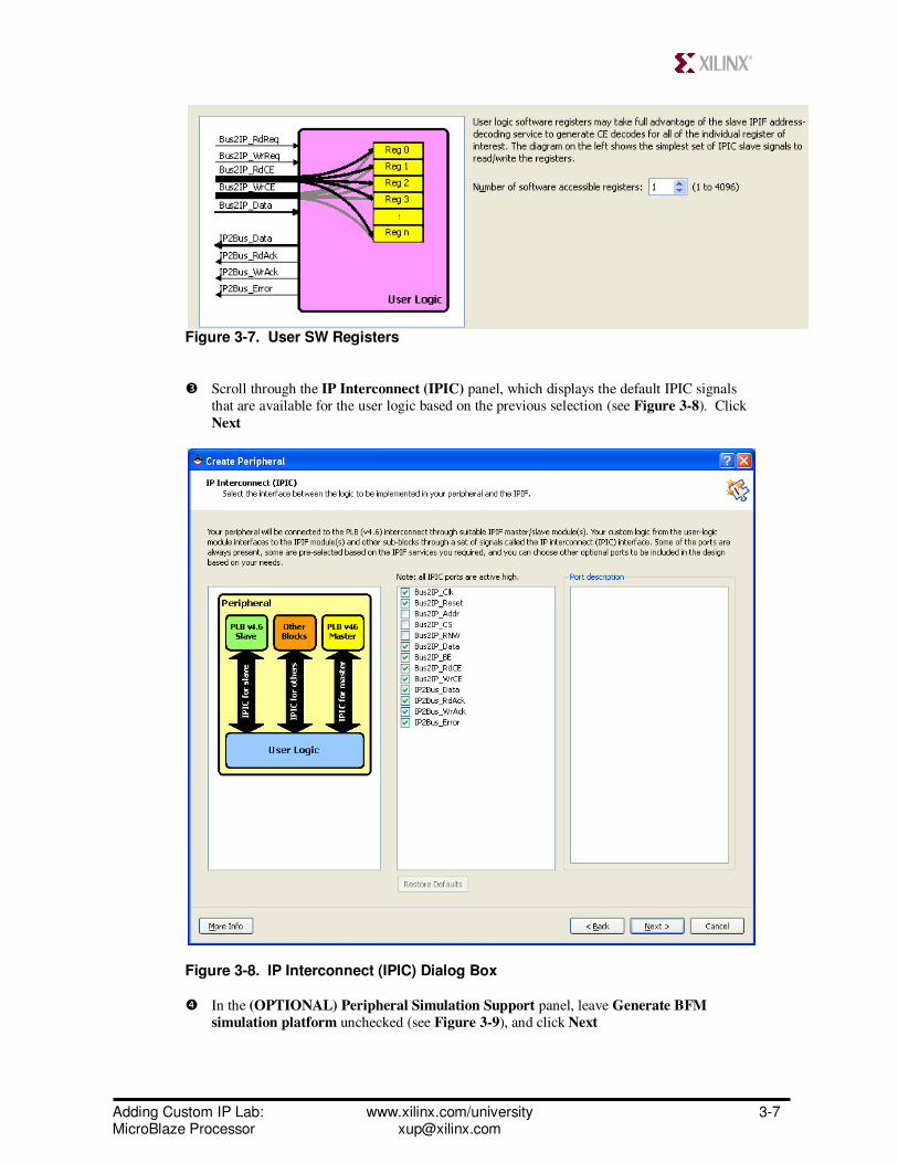
Adding Custom IP Lab: www.xilinx.com/university 3-7 MicroBlaze Processor [email protected]
Figure 3-7. User SW Registers
� Scroll through the IP Interconnect (IPIC) panel, which displays the default IPIC signals
that are available for the user logic based on the previous selection (see Figure 3-8). Click
Next
Figure 3-8. IP Interconnect (IPIC) Dialog Box
� In the (OPTIONAL) Peripheral Simulation Support panel, leave Generate BFM
simulation platform unchecked (see Figure 3-9), and click Next
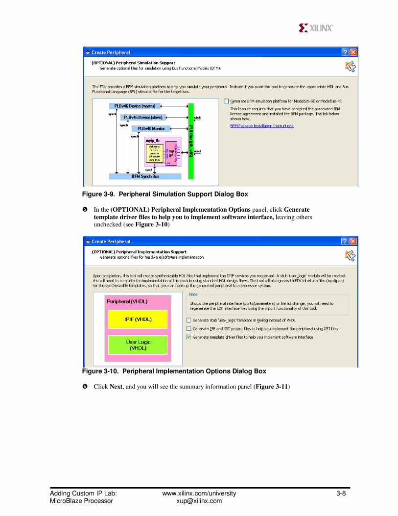
Adding Custom IP Lab: www.xilinx.com/university 3-8 MicroBlaze Processor [email protected]
Figure 3-9. Peripheral Simulation Support Dialog Box
� In the (OPTIONAL) Peripheral Implementation Options panel, click Generate
template driver files to help you to implement software interface, leaving others unchecked (see Figure 3-10)
Figure 3-10. Peripheral Implementation Options Dialog Box
� Click Next, and you will see the summary information panel (Figure 3-11)
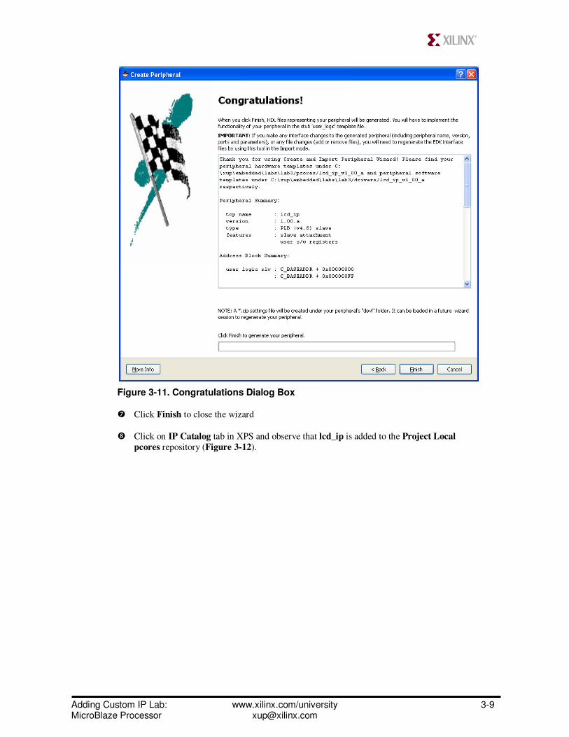
Adding Custom IP Lab: www.xilinx.com/university 3-9 MicroBlaze Processor [email protected]
Figure 3-11. Congratulations Dialog Box
� Click Finish to close the wizard
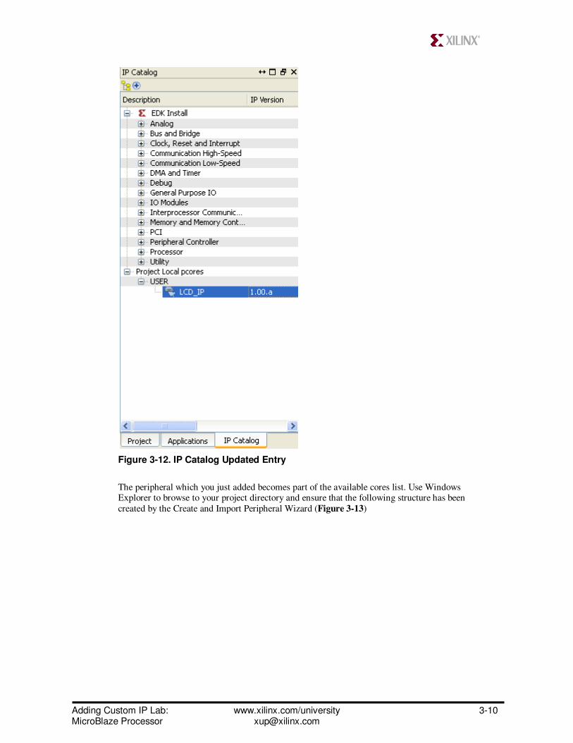
� Click on IP Catalog tab in XPS and observe that lcd_ip is added to the Project Local
pcores repository (Figure 3-12).
Adding Custom IP Lab: www.xilinx.com/university 3-10 MicroBlaze Processor [email protected]
Figure 3-12. IP Catalog Updated Entry
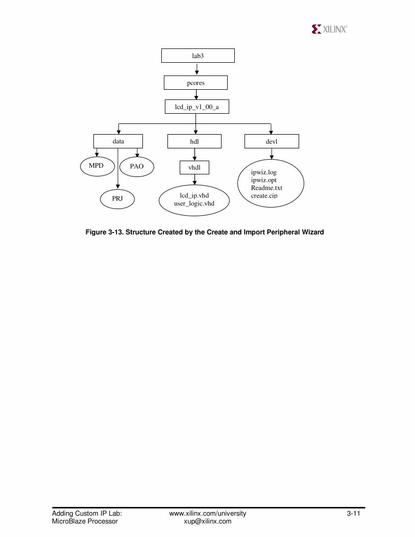
The peripheral which you just added becomes part of the available cores list. Use Windows Explorer to browse to your project directory and ensure that the following structure has been
created by the Create and Import Peripheral Wizard (Figure 3-13)
Adding Custom IP Lab: www.xilinx.com/university 3-11 MicroBlaze Processor [email protected]
Figure 3-13. Structure Created by the Create and Import Peripheral Wizard
lab3
lcd_ip_v1_00_a
data hdl
vhdl MPD PAO
pcores
devl
ipwiz.log
ipwiz.opt
Readme.txt
create.cip PRJ lcd_ip.vhd
user_logic.vhd

Adding Custom IP Lab: www.xilinx.com/university 3-12 MicroBlaze Processor [email protected]
Create the Peripheral Step 3
Update the MPD file to include the lcd data output of the LCD controller
peripheral so the port can be connected in XPS.
Add a port called “lcd” to the MPD file.
� Open lcd_ip_v2_1_0.mpd in the pcores\lcd_ip_v1_00_a\data under lab3 directory.
� Add following line before the SPLB_Clk port under the Ports section
PORT lcd="",DIR=O,VEC=[0:6]
Figure 3-14. Update the MPD file for the LCD Controller Peripheral
� Save the file and close
Create the LCD controller using the appropriate HDL template files generated
from the Create/Import peripheral wizard: lcd_ip.vhd and user_logic.vhd. You
can edit these files using a standard text editor.
� Open lcd_ip.vhd in the pcores\ lcd_ip_v1_00_a\hdl\vhdl directory.
� Add user port lcd of width 7 under USER ports added here token (see Figure 3-15)

Adding Custom IP Lab: www.xilinx.com/university 3-13 MicroBlaze Processor [email protected]
Figure 3-15. Add the User Port LCD
� Search for next --USER and add port mapping statement, save the file and then close it
Figure 3-16. Add Port Mapping Statement
� Open user_logic.vhd file from the vhdl directory and add lcd port definition in the USER
Ports area

Adding Custom IP Lab: www.xilinx.com/university 3-14 MicroBlaze Processor [email protected]
Figure 3-17. Add the lcd Port Definition
� Search for next --USER and the enter the internal signal declaration according to the figure below
Figure 3-18. Internal Signal Declaration for the User Logic
� Search for –USER logic implementation and add the following code or copy it from
lab3_user_logic.vhd file located at c:\xup\embedded\source directory

Adding Custom IP Lab: www.xilinx.com/university 3-15 MicroBlaze Processor [email protected]
Figure 3-19. Add Code
� Save changes and close the user_logic.vhd
Select Project → Rescan User Repositories to have the changes in effect

Adding Custom IP Lab: www.xilinx.com/university 3-16 MicroBlaze Processor [email protected]
Add and Connect the Peripheral Step 4
Add and connect the LCD peripheral to the PLB bus in the System Assembly
View. Make internal and external port connections. Assign an address range to
it. Establish the LCD data port as external FPGA pins and assign the pin
location constraints so the peripheral interfaces to the LCD display on the
Spartan-3E starter kit.
� In IP Catalog, select lcd_ip core, drag and drop it in the System Assembly View panel.
Click OK to accept the default settings
� Make sure that the Bus Interfaces filter is selected in the System Assembly View and click
on the circle in the bus connection diagram to make bus connection (Figure 3-20)
Figure 3-20. Making Bus Connection
� Select the Ports filter, and connect the lcd port of the lcd_ip_0 instance as an external pin
by selecting Make External (Figure 3-21)
Figure 3-21. Assign the lcd_0 Instance
� Select Addresses filter and click the Generate Addresses button.
Your results should look similar to that below (as shown in Figure 3-22)

Adding Custom IP Lab: www.xilinx.com/university 3-17 MicroBlaze Processor [email protected]
Figure 3-22. Generate Addresses
Modify the system.ucf file to assign external LCD controller connections to the
proper FPGA pin locations.
� Open the system.ucf file by double-clicking the UCF File: data\system.ucf entry under
Project Files in the System tab
� Open the C:\xup\embedded\sources\lab3.ucf file and copy the pin assignments into the ucf
Figure 3-23. Adding UCF Constraints
� Save and close the file
Adding Custom IP Lab: www.xilinx.com/university 3-18 MicroBlaze Processor [email protected]
Verify the Design in Hardware Step 5
Add a software new software program. Use EDK to generate the configuration
file and program the Spartan-3E xc3s500e-4fg320 device.
� Click on the Applications tab and remove lab2.c file from the sources
� Add lab3.c file in sources from C:\xup\embedded\sources folder
� Open lab3.c and add space anywhere in white space and then save the file so new
timestamp occurs
� Connect the USB and RS-232 cables to the Spartan-3E Starter kit and power it up.
� Start a HyperTerminal with the following settings
• Baud rate: 115200
• Data bits: 8
• Parity: none
• Stop bits: 1
• Flow control: none
� From EDK, click on Device Configuration Download Bitstream to download the system to the FPGA
Note: this will perform the following steps
� Run platgen to generate the netlists
� Generate the bitstream
� Run libgen to generate the libraries and drivers
� Compile the program to generate the executable
� Update the BRAMs in the bitstream with the executable
� Download the bitstream to the FPGA
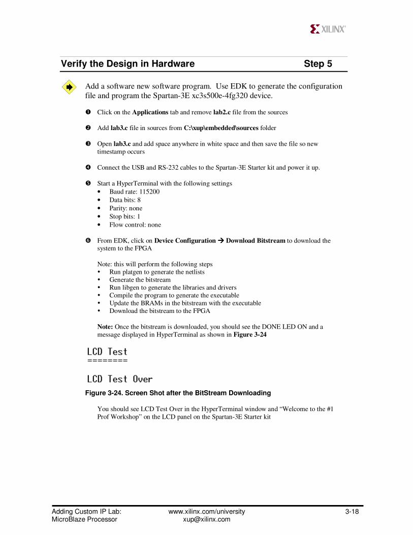
Note: Once the bitstream is downloaded, you should see the DONE LED ON and a
message displayed in HyperTerminal as shown in Figure 3-24
Figure 3-24. Screen Shot after the BitStream Downloading
You should see LCD Test Over in the HyperTerminal window and “Welcome to the #1
Prof Workshop” on the LCD panel on the Spartan-3E Starter kit

Adding Custom IP Lab: www.xilinx.com/university 3-19 MicroBlaze Processor [email protected]
Conclusion
The Create and Import Peripheral Wizard was used to create peripheral templates for the PLB bus. Logic was added to the templates to create an LCD interface peripheral. The peripheral
was then integrated into an existing processor system and tested in hardware using a provided
software application to display a message on the on-board LCD.

Adding Custom IP Lab: www.xilinx.com/university 3-20 MicroBlaze Processor [email protected]
Completed MHS File
# ##############################################################################
# Created by Base System Builder Wizard for Xilinx EDK 12.2 Build EDK_MS2.63c
# Tue Jul 20 10:08:16 2010 # Target Board: Xilinx Spartan-3E Starter Board Rev D
# Family: spartan3e
# Device: XC3S500e
# Package: FG320
# Speed Grade: -4
# Processor number: 1
# Processor 1: microblaze_0
# System clock frequency: 50.0
# Debug Interface: On-Chip HW Debug Module
# ##############################################################################
PARAMETER VERSION = 2.1.0
PORT fpga_0_RS232_DCE_RX_pin = fpga_0_RS232_DCE_RX_pin, DIR = I
PORT fpga_0_RS232_DCE_TX_pin = fpga_0_RS232_DCE_TX_pin, DIR = O
PORT fpga_0_LEDs_8Bit_GPIO_IO_O_pin = fpga_0_LEDs_8Bit_GPIO_IO_O_pin, DIR = O, VEC =
[0:7]
PORT fpga_0_DDR_SDRAM_DDR_Clk_pin = fpga_0_DDR_SDRAM_DDR_Clk_pin, DIR = O
PORT fpga_0_DDR_SDRAM_DDR_Clk_n_pin = fpga_0_DDR_SDRAM_DDR_Clk_n_pin, DIR = O
PORT fpga_0_DDR_SDRAM_DDR_CE_pin = fpga_0_DDR_SDRAM_DDR_CE_pin, DIR = O
PORT fpga_0_DDR_SDRAM_DDR_CS_n_pin = fpga_0_DDR_SDRAM_DDR_CS_n_pin, DIR = O
PORT fpga_0_DDR_SDRAM_DDR_RAS_n_pin = fpga_0_DDR_SDRAM_DDR_RAS_n_pin, DIR =
O PORT fpga_0_DDR_SDRAM_DDR_CAS_n_pin = fpga_0_DDR_SDRAM_DDR_CAS_n_pin, DIR =
O
PORT fpga_0_DDR_SDRAM_DDR_WE_n_pin = fpga_0_DDR_SDRAM_DDR_WE_n_pin, DIR = O
PORT fpga_0_DDR_SDRAM_DDR_BankAddr_pin = fpga_0_DDR_SDRAM_DDR_BankAddr_pin,
DIR = O, VEC = [1:0]
PORT fpga_0_DDR_SDRAM_DDR_Addr_pin = fpga_0_DDR_SDRAM_DDR_Addr_pin, DIR = O,
VEC = [12:0]
PORT fpga_0_DDR_SDRAM_DDR_DQ_pin = fpga_0_DDR_SDRAM_DDR_DQ_pin, DIR = IO,
VEC = [15:0]
PORT fpga_0_DDR_SDRAM_DDR_DM_pin = fpga_0_DDR_SDRAM_DDR_DM_pin, DIR = O,
VEC = [1:0] PORT fpga_0_DDR_SDRAM_DDR_DQS_pin = fpga_0_DDR_SDRAM_DDR_DQS_pin, DIR = IO,
VEC = [1:0]
PORT fpga_0_DDR_SDRAM_ddr_dqs_div_io_pin = fpga_0_DDR_SDRAM_ddr_dqs_div_io_pin,
DIR = IO
PORT fpga_0_clk_1_sys_clk_pin = dcm_clk_s, DIR = I, SIGIS = CLK, CLK_FREQ = 50000000
PORT fpga_0_rst_1_sys_rst_pin = sys_rst_s, DIR = I, SIGIS = RST, RST_POLARITY = 1
PORT push_GPIO_IO_I_pin = push_GPIO_IO_I, DIR = I, VEC = [0:3]
PORT dip_GPIO_IO_I_pin = dip_GPIO_IO_I, DIR = I, VEC = [0:3]
PORT lcd_ip_0_lcd_pin = lcd_ip_0_lcd, DIR = O, VEC = [0:6]
BEGIN microblaze
PARAMETER INSTANCE = microblaze_0
PARAMETER C_AREA_OPTIMIZED = 1

Adding Custom IP Lab: www.xilinx.com/university 3-21 MicroBlaze Processor [email protected]
PARAMETER C_DEBUG_ENABLED = 1
PARAMETER HW_VER = 7.30.b
BUS_INTERFACE DLMB = dlmb
BUS_INTERFACE ILMB = ilmb
BUS_INTERFACE DPLB = mb_plb
BUS_INTERFACE IPLB = mb_plb BUS_INTERFACE DEBUG = microblaze_0_mdm_bus
PORT MB_RESET = mb_reset
END
BEGIN plb_v46
PARAMETER INSTANCE = mb_plb
PARAMETER HW_VER = 1.04.a
PORT PLB_Clk = clk_50_0000MHz
PORT SYS_Rst = sys_bus_reset
END
BEGIN lmb_v10 PARAMETER INSTANCE = ilmb
PARAMETER HW_VER = 1.00.a
PORT LMB_Clk = clk_50_0000MHz
PORT SYS_Rst = sys_bus_reset
END
BEGIN lmb_v10
PARAMETER INSTANCE = dlmb
PARAMETER HW_VER = 1.00.a
PORT LMB_Clk = clk_50_0000MHz
PORT SYS_Rst = sys_bus_reset END
BEGIN lmb_bram_if_cntlr
PARAMETER INSTANCE = dlmb_cntlr
PARAMETER HW_VER = 2.10.b
PARAMETER C_BASEADDR = 0x00000000
PARAMETER C_HIGHADDR = 0x00001fff
BUS_INTERFACE SLMB = dlmb
BUS_INTERFACE BRAM_PORT = dlmb_port
END
BEGIN lmb_bram_if_cntlr PARAMETER INSTANCE = ilmb_cntlr
PARAMETER HW_VER = 2.10.b
PARAMETER C_BASEADDR = 0x00000000
PARAMETER C_HIGHADDR = 0x00001fff
BUS_INTERFACE SLMB = ilmb
BUS_INTERFACE BRAM_PORT = ilmb_port
END
BEGIN bram_block
PARAMETER INSTANCE = lmb_bram
PARAMETER HW_VER = 1.00.a BUS_INTERFACE PORTA = ilmb_port
BUS_INTERFACE PORTB = dlmb_port
END

Adding Custom IP Lab: www.xilinx.com/university 3-22 MicroBlaze Processor [email protected]
BEGIN xps_uartlite
PARAMETER INSTANCE = RS232_DCE
PARAMETER C_BAUDRATE = 115200
PARAMETER C_DATA_BITS = 8
PARAMETER C_USE_PARITY = 0
PARAMETER C_ODD_PARITY = 0 PARAMETER HW_VER = 1.01.a
PARAMETER C_BASEADDR = 0x84000000
PARAMETER C_HIGHADDR = 0x8400ffff
BUS_INTERFACE SPLB = mb_plb
PORT RX = fpga_0_RS232_DCE_RX_pin
PORT TX = fpga_0_RS232_DCE_TX_pin
END
BEGIN xps_gpio
PARAMETER INSTANCE = LEDs_8Bit
PARAMETER C_ALL_INPUTS = 0
PARAMETER C_GPIO_WIDTH = 8 PARAMETER C_INTERRUPT_PRESENT = 0
PARAMETER C_IS_DUAL = 0
PARAMETER HW_VER = 2.00.a
PARAMETER C_BASEADDR = 0x81440000
PARAMETER C_HIGHADDR = 0x8144ffff
BUS_INTERFACE SPLB = mb_plb
PORT GPIO_IO_O = fpga_0_LEDs_8Bit_GPIO_IO_O_pin
END
BEGIN mpmc
PARAMETER INSTANCE = DDR_SDRAM PARAMETER C_NUM_PORTS = 1
PARAMETER C_SPECIAL_BOARD = S3E_STKIT
PARAMETER C_MEM_TYPE = DDR
PARAMETER C_MEM_PARTNO = MT46V32M16-6
PARAMETER C_MEM_DATA_WIDTH = 16
PARAMETER C_PIM0_BASETYPE = 2
PARAMETER HW_VER = 6.01.a
PARAMETER C_MPMC_BASEADDR = 0x8c000000
PARAMETER C_MPMC_HIGHADDR = 0x8fffffff
BUS_INTERFACE SPLB0 = mb_plb
PORT MPMC_Clk0 = clk_100_0000MHzDCM0
PORT MPMC_Clk90 = clk_100_0000MHz90DCM0 PORT MPMC_Rst = sys_periph_reset
PORT DDR_Clk = fpga_0_DDR_SDRAM_DDR_Clk_pin
PORT DDR_Clk_n = fpga_0_DDR_SDRAM_DDR_Clk_n_pin
PORT DDR_CE = fpga_0_DDR_SDRAM_DDR_CE_pin
PORT DDR_CS_n = fpga_0_DDR_SDRAM_DDR_CS_n_pin
PORT DDR_RAS_n = fpga_0_DDR_SDRAM_DDR_RAS_n_pin
PORT DDR_CAS_n = fpga_0_DDR_SDRAM_DDR_CAS_n_pin
PORT DDR_WE_n = fpga_0_DDR_SDRAM_DDR_WE_n_pin
PORT DDR_BankAddr = fpga_0_DDR_SDRAM_DDR_BankAddr_pin
PORT DDR_Addr = fpga_0_DDR_SDRAM_DDR_Addr_pin
PORT DDR_DQ = fpga_0_DDR_SDRAM_DDR_DQ_pin PORT DDR_DM = fpga_0_DDR_SDRAM_DDR_DM_pin
PORT DDR_DQS = fpga_0_DDR_SDRAM_DDR_DQS_pin
PORT DDR_DQS_Div_O = fpga_0_DDR_SDRAM_ddr_dqs_div_io_pin
PORT DDR_DQS_Div_I = fpga_0_DDR_SDRAM_ddr_dqs_div_io_pin

Adding Custom IP Lab: www.xilinx.com/university 3-23 MicroBlaze Processor [email protected]
END
BEGIN clock_generator
PARAMETER INSTANCE = clock_generator_0
PARAMETER C_CLKIN_FREQ = 50000000
PARAMETER C_CLKOUT0_FREQ = 100000000 PARAMETER C_CLKOUT0_PHASE = 90
PARAMETER C_CLKOUT0_GROUP = DCM0
PARAMETER C_CLKOUT0_BUF = TRUE
PARAMETER C_CLKOUT1_FREQ = 100000000
PARAMETER C_CLKOUT1_PHASE = 0
PARAMETER C_CLKOUT1_GROUP = DCM0
PARAMETER C_CLKOUT1_BUF = TRUE
PARAMETER C_CLKOUT2_FREQ = 50000000
PARAMETER C_CLKOUT2_PHASE = 0
PARAMETER C_CLKOUT2_GROUP = NONE
PARAMETER C_CLKOUT2_BUF = TRUE
PARAMETER C_EXT_RESET_HIGH = 1 PARAMETER HW_VER = 4.00.a
PORT CLKIN = dcm_clk_s
PORT CLKOUT0 = clk_100_0000MHz90DCM0
PORT CLKOUT1 = clk_100_0000MHzDCM0
PORT CLKOUT2 = clk_50_0000MHz
PORT RST = sys_rst_s
PORT LOCKED = Dcm_all_locked
END
BEGIN mdm
PARAMETER INSTANCE = mdm_0 PARAMETER C_MB_DBG_PORTS = 1
PARAMETER C_USE_UART = 1
PARAMETER C_UART_WIDTH = 8
PARAMETER HW_VER = 1.00.g
PARAMETER C_BASEADDR = 0x84400000
PARAMETER C_HIGHADDR = 0x8440ffff
BUS_INTERFACE SPLB = mb_plb
BUS_INTERFACE MBDEBUG_0 = microblaze_0_mdm_bus
PORT Debug_SYS_Rst = Debug_SYS_Rst
END
BEGIN proc_sys_reset PARAMETER INSTANCE = proc_sys_reset_0
PARAMETER C_EXT_RESET_HIGH = 1
PARAMETER HW_VER = 2.00.a
PORT Slowest_sync_clk = clk_50_0000MHz
PORT Ext_Reset_In = sys_rst_s
PORT MB_Debug_Sys_Rst = Debug_SYS_Rst
PORT Dcm_locked = Dcm_all_locked
PORT MB_Reset = mb_reset
PORT Bus_Struct_Reset = sys_bus_reset
PORT Peripheral_Reset = sys_periph_reset
END
BEGIN xps_gpio
PARAMETER INSTANCE = dip
PARAMETER HW_VER = 2.00.a

Adding Custom IP Lab: www.xilinx.com/university 3-24 MicroBlaze Processor [email protected]
PARAMETER C_GPIO_WIDTH = 4
PARAMETER C_ALL_INPUTS = 1
PARAMETER C_BASEADDR = 0x81420000
PARAMETER C_HIGHADDR = 0x8142ffff
BUS_INTERFACE SPLB = mb_plb
PORT GPIO_IO_I = dip_GPIO_IO_I END
BEGIN xps_gpio
PARAMETER INSTANCE = push
PARAMETER HW_VER = 2.00.a
PARAMETER C_GPIO_WIDTH = 4
PARAMETER C_ALL_INPUTS = 1
PARAMETER C_BASEADDR = 0x81400000
PARAMETER C_HIGHADDR = 0x8140ffff
BUS_INTERFACE SPLB = mb_plb
PORT GPIO_IO_I = push_GPIO_IO_I
END
BEGIN lcd_ip
PARAMETER INSTANCE = lcd_ip_0
PARAMETER HW_VER = 1.00.a
PARAMETER C_BASEADDR = 0xcf400000
PARAMETER C_HIGHADDR = 0xcf40ffff
BUS_INTERFACE SPLB = mb_plb
PORT lcd = lcd_ip_0_lcd
END


![[DCS BLACK SHARK ADDING CUSTOM SKINS] February … BS_How … · KA-50 templates (available from DCS) ... RCN_Moose | Version 1.0 26 ... [DCS BLACK SHARK – ADDING CUSTOM SKINS]](https://img.pdfslide.us/doc/110x75/5b2acbaa7f8b9a55068b909a/dcs-black-shark-adding-custom-skins-february-bshow-ka-50-templates-available.jpg)