Embed Size (px)
Citation preview

16-09-27 TSTE25
Lab 2 1(19)
Tomas Jonsson
LINKÖPING UNIVERSITY ICS/ISY
Lab 2 Power electronics
Contents
Introduction ................................................................................................................ 1
Initial setup ................................................................................................................. 2
Starting the software ................................................................................................... 2
Notes on the schematics .............................................................................................. 2
Simulating the design .................................................................................................. 2
Existing simulation variables .................................................................................. 3
Extra measurement points ...................................................................................... 3
Presentation and analysis of the result ....................................................................... 3
Lab 2-1 Ideal full-bridge inverter with unipolar switching ......................................... 5
Multisim model ....................................................................................................... 5
Circuit description ................................................................................................... 5
Lab 2-1a Converter design ...................................................................................... 8
Lab 2-1b Design calculations .................................................................................. 8
Lab 2-1c Measurements .......................................................................................... 8
Reference ................................................................................................................ 8
Lab 2-2 MOSFET based full-bridge inverter with optimized gate drive .....................9
PWM control ......................................................................................................... 10
Gate pulse interlocking .......................................................................................... 11
Gate drive circuits .................................................................................................. 12
Inverter main circuit ............................................................................................. 14
Converter ratings ................................................................................................... 15
Lab 2-2a Performance calculations ....................................................................... 15
Lab 2-2b Measurements ........................................................................................ 16
Multisim simulation options ..................................................................................... 18
Datasheets ................................................................................................................. 19
Introduction
This lab focus on simulation and evaluation of the full-bridge AC/DC inverter structure.
Simulations should be performed, using predefined models.

LINKÖPING UNIVERSITY ICS/ISY
TSTE25 Lab 2 2(19)
Initial setup
The design files used in the lab can be copied from
/site/edu/eks/TSTE19/current/material/Lab2_files in Linux or from
U:\eks\current\TSTE19\material\Lab2_files in Windows. Put the copied files into
your home directory, for example in /edu/<userid>/TSTE19/ on Linux or H:\TSTE19 on
Windows.
Please note that the software only works on Windows. You can thus only run the
software in the Freja and Transistorn labs.
Starting the software
The software is started by Start ->All Programs ->National Instruments ->Circuit
Design Suite 14.0 ->Multisim 14.0
Open the corresponding design project using File->Open and select the design file to
use among the files you copied in the initial setup.
Notes on the schematics
Some of the schematics have more components added than shown in the tasks in the
book. One reason for these (typically small resistances and inductances) are the
computational properties of the simulation model. Without the extra components, the
simulation calculations could become unsolvable.
Names and values of components can be changed by double-clicking on the
value/name. Alternatively, the names and values can be changed by right-clicking on the
component and select Properties.
Additional measures can be added by introducing the Measurement probe, which is a
yellow symbol at the bottom of the column of symbols on the right side of the window.
Place the cursor on top of the symbol to see the name of that particular symbol. Click on
it and then click on a wire in the schematic to add a measurement probe to the
schematic.
One useful variable for the following analysis step is a time variable. The Multisim
environment does not directly support such a variable, but it can easily be added in one
of many ways. The approach taken in the existing simulation models are the use of
voltage source that increments its output voltage linearly at the rate of 1 V per second.
The voltage value is then the same as the time value, as long as the maximum time is
not exceeded.
Simulating the design
Simulation of the design can be done using different analysis configurations. The ones
used in this lab will be transient and Fourier analysis.

LINKÖPING UNIVERSITY ICS/ISY
TSTE25 Lab 2 3(19)
The analysis (and simulation) of the design is started by selecting
Simulate->Analysis->Transient analysis or Simulate->Analysis->Fourier analysis
respectively. This will start the simulator, which will store the waveforms of all nodes in
the circuit for future presentation. The simulator opens a new window named Graph
View, in which all waveforms are presented.
Existing simulation variables
All voltages and currents in the circuit are available after simulation. The voltages at
individual nodes are accessed using the names V(1) etc. All nodes are either named
explicitly or enumerated and shown as a red text or digit in the schematic. I(Rs) gives
the current entering Rs. The currents usually are assuming the positive current entering
the 1st pin of the symbol.
Plotting the voltage across a given component is then done by calculating the voltage
difference between the node voltages the component is connected to.
Extra measurement points
Additional measurements of voltage and current can be added through placing
probes in the Multisim circuit by selecting
Place->Probe->Voltage (Current or Differential voltage).
OBS these probes cannot be used for harmonic Fourier analysis.
Presentation and analysis of the result
The Graph View window presents the waveforms of some selected voltages and
currents. Individual traces can be disabled by deselecting the corresponding white box
at the bottom of the window.
New traces can be added using Graph->Add trace(s) from latest simulation result. In
the resulting dialog window additional traces can be added to the existing graph, or to a
new graph. Select the trace of interest, press Copy variable to expression, then press
Calculate.
Beside currents, node voltages and power traces, additional traces can be calculated
using mathematical expression. Among the simplest examples of this is the calculation
of the voltage across a component. E. g., if a component is connected between nodes 3
and 5 (assuming + on node 3), the voltage across that component is then calculated
using the expression V(3) – V(5).
Other functions may also be used, such as RMS and AVG, which calculates the rms and
average values respectively of a signal or expression. Example: RMS(V(1)).
Note that these calculations is made on the calculated waveform, and is therefore
different at different times, as the calculation is not performed on an infinite long
waveform.
Arbitrary mathematical functions can also be plotted by the use of a time variable (using

LINKÖPING UNIVERSITY ICS/ISY
TSTE25 Lab 2 4(19)
the voltage of a triangle wave voltage source). A sinusoidal waveform of 10 V, 50 Hz
with a phase shift of 45 degrees can be plotted using the trace entry
10*sin(2*pi*50*V(time)+45*pi/180). Note that the angles are always described in
radians.
The Fourier transform can be calculated on signals and expressions. Select
Simulate->Analysis->Fourier analysis. Set the fundamental frequency, number of
harmonics, and stop time for sampling. Select the output tab, and add there the variables
and expressions that will have their Fourier series coefficients calculated. Finally, press
Simulate. The simulation is now run, and the simulation result is used to calculate the
Fourier series coefficients and then present them together with details about DC
component and distortion factor THD in the Graph View window.
Waveform results can be copied using Edit->Copy graph to clipboard and then pasted
into a LibreOffice or Wordpad document or Paint for editing.
LINKÖPING UNIVERSITY ICS/ISY
TSTE25 Lab 2 5(19)
Lab 2-1 Ideal full-bridge inverter with unipolar
switching
Multisim model
Load the model FB_inv_unipol.ms4.
Circuit description
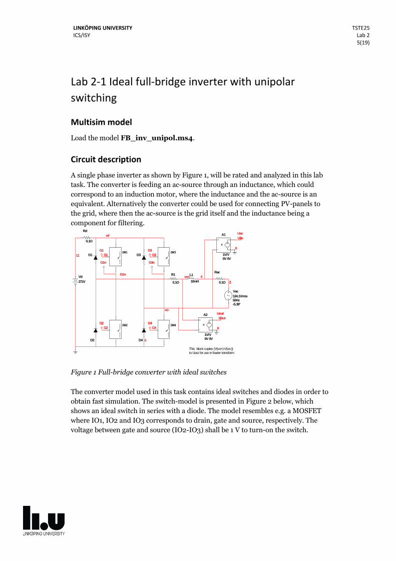
A single phase inverter as shown by Figure 1, will be rated and analyzed in this lab
task. The converter is feeding an ac-source through an inductance, which could
correspond to an induction motor, where the inductance and the ac-source is an
equivalent. Alternatively the converter could be used for connecting PV-panels to
the grid, where then the ac-source is the grid itself and the inductance being a
component for filtering.
Figure 1 Full-bridge converter with ideal switches
The converter model used in this task contains ideal switches and diodes in order to
obtain fast simulation. The switch-model is presented in Figure 2 below, which
shows an ideal switch in series with a diode. The model resembles e.g. a MOSFET
where IO1, IO2 and IO3 corresponds to drain, gate and source, respectively. The
voltage between gate and source (IO2-IO3) shall be 1 V to turn-on the switch.
Vd
271V
L1
10mH
Rac
0.1O
D1
D2
D3
D4
SW3
SW4G4
G4
G3
G3SW1
SW2
0
G1
G1
G2
G2
Vac
124.1Vrms 50Hz -5.39°
2
A1
1V/V 0V 0V
+-
K
+
-
Uac
Uac
0
4
G1n G3n
Rd
0.1O
11
vd
A2
1V/V 0V 0V
+-
K
+
-
vo-
0
Uout
Uout
R1
0.1O
vo+G1n
This block copies (V(vo+)-V(vo-)) to Uout for use in fourier transform

LINKÖPING UNIVERSITY ICS/ISY
TSTE25 Lab 2 6(19)
Figure 2 Switch model
The pulse width modulation used here is unipolar with a switching frequency of
950Hz. This gives a frequency modulation ratio of 19, related to the fundamental
frequency of 50 Hz. The PWM is defined as shown by Figure 3, giving the gate
signals G1-G4 to define the turn-on and turn-off of the switches.
Figure 3 Unipolar PWM control
The PWM reference is defined by the signal Vctrl, which has an amplitude
corresponding to the desired amplitude modulation index, ma. In Figure 4 below the
signal Vctrl and the PWM carrier, Vtri is shown.
Figure 4 PWM reference and carrier
Looking inside the blocks SC1 and SC3 reveals the creation of the Gate pulses. Here
the output signals IO1 and IO2 correspond to G1 and G2 in block SC1 and G3 and
G4 in block SC3, respectively.
S2
+-
IO1
IO2
IO3
G1
D2
vo+
vd
9
V3
0.8Vpk 50Hz 0°
SC1
pwm_tri
IO1
IO2
Vctrl
Vtri
SC3
pwm_tri
IO1
IO2
Vctrl
Vtri
G4G4
G3
G3
G1
G1 G2G2
V4
2V 1.053ms
0
Vtri
A3
-1V/V
IN OUTVctrl_inv
Vctrl

LINKÖPING UNIVERSITY ICS/ISY
TSTE25 Lab 2 7(19)
Figure 5 Gate pulse generation
The time instant of the gate pulse is defined by the comparators U1 and U2 which
changes from logical 0 to a logical 1 output when the signal Vctrl exceeds Vtri. The
gate signals G1 and G2 shall generally be the inverse to the other. However, in order
to ensure both switches in a leg is conducting simultaneously, a blanking interval is
introduced. The blanking implies, that the turn-off of one switch is done before
turning on the other as shown below.
Figure 6 PWM and gate pulse waveform
The blanking is accomplished in this case by introducing an offset in comparator
U1. The final gate pulses that are connected to the switches of the converter from
the PWM circuit is sent through voltage controlled voltage generators in order to
overcome the potential shift of switch 1 and 3 (Sw1 & SW3). The lower terminal of
Sw1 (G1n) will when Sw2 is off, be at a potential corresponding to Vd. In Figure 6
above the voltage signal between G1 and G1n is shown together with G2. G2
connection to Sw2 (and G4 to Sw4) does not pose any problem with potential shift
since these lower switches are connected with the source directly to ground.
V5
PWL
V6
PWL
IO1
IO2
Vctrl
G1
U1
G2
0
3
U2
Vctrl
1
0
VtriVtri
IO1nvo+

LINKÖPING UNIVERSITY ICS/ISY
TSTE25 Lab 2 8(19)
Lab 2-1a Converter design
The model in FB_inv_unipol.ms4 shall be updated with respect to the circuit
parameters. Follow the design steps listed below:
1. Ac-voltage: Vac1 = 230 Vrms, 50 Hz, 0 deg
2. Select a dc-voltage, Vd, to get ma=0.9 at the given ac-voltage.
3. Define the rated fundamental ac-side current, IL1, corresponding to 2000
VA (2000 W at cos(fi)=1)
4. Define a series inductance giving 10% of the base impedance (𝑍𝑏 =𝑉𝑎𝑐1
𝐼𝐿1)
at 50Hz. XL =0.1 Zb
5. Set the PWM reference (Vctrl) for ma=0.9 and a phase angle = 0.
Lab 2-1b Design calculations
Calculate the magnitude and phase of the fundamental current component on the
ac-side. Consider the following equation:
𝐼�̅�1 =�̂�𝑜𝑢𝑡𝑒
𝑗𝜑𝑜𝑢𝑡 − �̂�𝑎𝑐𝑒𝑗𝜑𝑎𝑐
𝑗𝜔𝐿
Lab 2-1c Measurements
Using the model with the modified converter parameters above, perform the
following measurements when the converter has reached a stable steady state. If
convergence problems occur consider the recommendations in section “Multisim
simulation options”:
1. Magnitude and phase of the fundamental frequency ac-side current
component (current through L1).
2. Peak ac-side current I(L1).
3. Magnitude and phase of the fundamental frequency component of the
switched output voltage, Vout.
4. Spectra of Vout. Use Fourier function to get up to the 100th harmonic.
5. Spectra of ac-current through L1. Use Fourier function to get up to the
100th harmonic.
6. Calculate active and reactive power that is fed into the ac-source (Vac).
7. Change amplitude and phase of the PWM reference (Vctrl) to get P=2 kW
and Q=0 Var into the ac-source. Use the amplitude and phase angle of
the current I(L1) together with the fixed ac-voltage to determine P and Q.
Reference
Section 8-3-2 in Mohan Power electronics

LINKÖPING UNIVERSITY ICS/ISY
TSTE25 Lab 2 9(19)
Lab 2-2 MOSFET based full-bridge inverter with
optimized gate drive
This task relates to a single phase full-bridge inverter similar to the one analysed in
task 2-1 above. This inverter is however based on detailed MOSFET and diode
models and with a more sophisticated gate drive circuitry.
A Multisim model is found in the Lab2 system folder as: inv_lab2.ms14
The Multisim model also needs the two additional files:
Inverter_circuit_Lab2.ms14 and NonOverlapping_Lab2.ms14 for
definition of sub-circuits. Note that only the main file needs to be loaded, the two
additional files shall reside in the same folder.
The model is hierarchical with the top level shown below. The top level includes
control references, the PWM control and the physical inverter circuit..
Figure 7 Front end with control references for the full-bridge inverter
Vdc
15V
Vref
0.9Vpk 50Hz
0°
Vtri
-1V 1V 0s 1.0ms
HB1
Inverter_circuit_Lab2
Vin
V_bs
g1g2
g3g4
DEBLSC7
PWM control
Vref_in
triangle_in
Vrefinv_ing1g2
g3g4
V1
2ms
Vdc_bs
15V
R5
0.1O
V2
1V/V
Deblock control

LINKÖPING UNIVERSITY ICS/ISY
TSTE25 Lab 2
10(19)
PWM control
The PWM control is given by the PWM control block as shown by Figure 8 below.
Figure 8 PWM control
The PWM is setup for unipolar switching where G1 and G2 corresponds to one leg of
the full-bridge converter and G3 and G4 of the other. The gate pulse G1 and G2 are
derived using the Vref_in signal while G3 and G4 referred to the inverse Vrefinv_in.
Blanking time is included through an offset of -0.05 in the comparators of G1 and
G3. Thereby the following expressions can be written corresponding to the gate
pulse generation:
G1 = Vref_in-0.05 > triangle_in
G2 = triangle_in > Vref_in
G3 = Vrefinv_in-0.05 > triangle_in
G4 = triangle_in > Vrefinv_in
Through the addition of the negative offset to Vref for G1 a blanking interval is
obtained with respect to G2. This is explained by the fact that for increasing triangle
wave, the intersection with Vref will come earlier through the negative offset,
resulting in G1 turn-off earlier than the G2 turn-on. The opposite applies to interval
with decreasing triangle wave, where the negative offset will delay the intersection
with Vref, resulting in a later G1 turn-on compared to the G2 turn-off.
g1
g2
g3
g4
U19
COMPARATOR_VIRTUAL
U20
COMPARATOR_VIRTUAL
U21
COMPARATOR_VIRTUAL
U22
COMPARATOR_VIRTUAL
Vref_in
triangle_in
Vrefinv_in

LINKÖPING UNIVERSITY ICS/ISY
TSTE25 Lab 2
11(19)
Figure 9 PWM
The blanking time obtained with the offset is defined by the rate of change of the
triangle wave according to the following equation:
𝑡𝑏𝑙𝑎𝑛𝑘 =|𝑜𝑓𝑓𝑠𝑒𝑡|
𝑑𝑉𝑡𝑟𝑖𝑑𝑡⁄
=|𝑜𝑓𝑓𝑠𝑒𝑡|
4𝑓𝑠
For fs = 1 kHz and an offset = -0.05 a blanking time of 12.5 µs is obtained.
Gate pulse interlocking
The next block after PWM control is “NonOverlapping” and contains logic to obtain
interlocking between G1/G2 and G3/G4 to prevent simultaneous on-state. When G1
is on, G2 must equal zero in order to permit turn-on through G1. The same applies
to the other combinations of G1 – G4. The logic also contains a deblock signal which
when equal to zero sets all gate pulses to off-state. Enabling of normal switching is
done with deblock=1.
0 0.2 0.4 0.6 0.8 1 1.2 1.4 1.6 1.8 2
x 10-3
-0.5
0
0.5
1
1.5
0 0.2 0.4 0.6 0.8 1 1.2 1.4 1.6 1.8 2
x 10-3
-1
-0.5
0
0.5
1
G1
G2
Tri
Vref
Vref-0.05

LINKÖPING UNIVERSITY ICS/ISY
TSTE25 Lab 2
12(19)
Figure 10 Gate pulse interlocking logics
Gate drive circuits
The PWM gate pulses are converted into the final gate-source voltage through the
circuit showed below:
Figure 11 gate drive overview
The gate drive blocks provide isolation in addition to the actual driving of the
required gate current for the proper turn-on and turn-off.
In1
In2
Out1
Out2
VCC
5.0V
DEBL
In3
In4
Out3
Out4
U4B
7404N
U4A
7404N
U4D
7404N
U4E
7404N
U5A
74F08N
U5B
74F08N
U5C
74F08N
U5D
74F08N
U6A
74F08N
U6B
74F08N
U6C
74F08N
U6D
74F08N
R7
270O
R19
270O
R24
270O
R12
270O
SC2
Gate_drive_top
V_sig V_go
V_bs
V_s
SC3
Gate_drive_top
V_sig V_go
V_bs
V_s
SC5
Gate_drive_bottom
V_sig
V_b
V_go
SC6
Gate_drive_bottom
V_sig
V_b
V_go
V_bs
V_bs
V_bs
V_bs
V_g1V_s1
V_g3V_s3
V_g2
V_g4
g1
g2
g3
g4
HB2
NonOverlapping_Lab2
In1In2
Out1Out2
DEBL
In3
In4
Out3Out4
DEBL
LINKÖPING UNIVERSITY ICS/ISY
TSTE25 Lab 2
13(19)
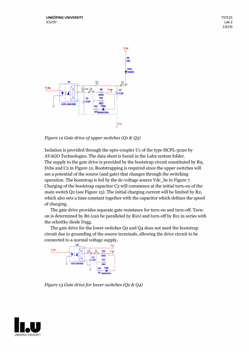
Figure 12 Gate drive of upper switches (Q1 & Q3)
Isolation is provided through the opto-coupler U1 of the type HCPL-3020 by
AVAGO Technologies. The data sheet is found in the Lab2 system folder.
The supply to the gate drive is provided by the bootstrap circuit constituted by R9,
D1bs and C2 in Figure 12. Bootstrapping is required since the upper switches will
see a potential of the source (and gate) that changes through the switching
operation. The bootstrap is fed by the dc-voltage source Vdc_bs in Figure 7.
Charging of the bootstrap capacitor C2 will commence at the initial turn-on of the
main switch Q2 (see Figure 15). The initial charging current will be limited by R2,
which also sets a time constant together with the capacitor which defines the speed
of charging.
The gate drive provides separate gate resistance for turn-on and turn-off. Turn-
on is determined by R6 (can be paralleled by R10) and turn-off by R11 in series with
the schottky diode D1gg.
The gate drive for the lower switches Q2 and Q4 does not need the bootstrap
circuit due to grounding of the source terminals, allowing the drive circuit to be
connected to a normal voltage supply.
Figure 13 Gate drive for lower switches (Q2 & Q4)
C2
4.7µF
V_go
V_bs
V_s
R6
1000O
V_sig
R9
10O
R11
10O
D1gg
SB160-E3/54
D1bs
1N4150
U1
HCPL-3020-000E
2
3
5
8
6
C5
0.1µF
R10
180O
I_bs1A
Ig1AVgg1V
V
V_b
V_goR18
1000O
V_sig
R20
10O
D2gg
SB160-E3/54
C11
0.1µF
U12
HCPL-3020-000E
2
3
5
8
6
R33
180O
Ig2A
Vgg2V

LINKÖPING UNIVERSITY ICS/ISY
TSTE25 Lab 2
14(19)
Inverter main circuit
The full-bridge inverter circuit is defined by the “Inverter_core” block in Figure 14,
where the following external terminals are found:
V_in: The dc-side voltage
V_op: The positive ac-output terminal
V_on: The negative ac-output terminal
The load is connected between V_op and V_on.
Figure 14
Inside “Inverter-core” the detailed full-bridge inverter circuit is defined as shown by
Figure 15
Figure 15 Full-bridge inverter circuit
The full-bridge is designed with MOSFET switches Q1-Q4 of type IRF540 by
VISHAY. An antiparallel diode is included with each MOSFET as D1-D4 of the type
BYW29E-200. The data sheets for the MOSFET and the diode is found in the Lab2
system folder.
SC1
Inverter_core
V_in
V_g2
V_g4
V_g3
V_g1
V_s1 V_on
V_op
V_s3
R2
10O
V_g1
V_g3
V_g2
V_g4
Vin_int
L1
50nH
V_s1
V_s3
L2
5mH
IloadA UloadV
V
V_in
V_g2
V_g4
V_g3V_g1
R1 R3
V_s1
V_on
Q1
Q4
Q3
Q2
V_op
D1
D2
D3
D4
V_s3
Iq1A
Iq2A
Vgs1V
A
A
A
V
V
V
V
V
V
V V
A
A

LINKÖPING UNIVERSITY ICS/ISY
TSTE25 Lab 2
15(19)
Converter ratings
The MOSFET based full-bridge converter described here has the following ratings:
Vd = 15 V
Vout (ma = 0.9) = 9.5 Vrms
Iout (Rload = 10 ohm, Lload = 5 mH, f1 = 50 Hz) = 0.83 Arms
Lab 2-2a Performance calculations
Related to the design presented for the MOSFET based full-bridge inverter, perform
the following calculations of some performance parameters:
1. Total initial inrush current into the bootstrap supply. Neglect the current
to the opto-isolated drive circuits HCPL-3020.
2. Time delay from deblock until normal switching. Check HCPL-3020
datasheet for minimum supply voltage level for startup. Check the first
switching instant of Q2 and Q4.
3. Total turn-on delay until the current begins in the drain-source (t1 in
Figure 16) related to drive circuit parameters (Rg, Ciss, HCPL-3020
output voltage and delay). Consider the time required to reach the
threshold voltage (Vth) of the MOSFET. Use datasheets [3], [5] and
application note [6] for reference. Ciss = CGS + CGD.
Figure 16 MOSFET turn-on
4. Calculate the dvds/dt (drain-source voltage) during turn-on. Use
MOSFET capacitance Crss=CGD for Vds=10V as given by a graph in the
datasheet. Consider the equivalent circuit below, which relates to the
plateau interval of the gate voltage as shown in Figure 16. The plateau

LINKÖPING UNIVERSITY ICS/ISY
TSTE25 Lab 2
16(19)
voltage VGP=5V for this calculation. Consider the equivalent circuit in
Figure 17.
Figure 17 Turn-on equivalent during Vds voltage fall interval tfv1
5. Calculate resulting Vgs for a MOSFET in off-state (say Q1 in Figure 15)
when the opposite switch (Q2) is turning on. Assume the Vds of the
MOSFET to be exposed by a positive dvds/dt as calculated in step 4
above. Consider the entire gate circuit from the HCPL-3020 driver to the
MOSFET. The actual output voltage of the HCPL-3020 corresponding to
off-state is given in the datasheet. Consider the equivalent circuit in
Figure 18.
Figure 18 Turn-off equivalent during Vds voltage raise interval trv1
Lab 2-2b Measurements
Make the following measurements from Multisim and present the graphs in a lab
report document. These measurements are completely related to the performance
calculations in 2-2a.
The simulation with this more detailed circuit is more critical when it comes to the
convergence in Multisim. Set the maximum time step (TMAX) = 10ns as described
in the section “Multisim simulation options”. Also use the custom analysis options
recommended.
Sub-task 1 and 2 are both related to the startup of the converter while sub-task 3-5
are related to MOSFET turn-on during normal switching.
1. Record during startup, the current and voltage of the bootstrap capacitor
related to the gate drive of MOSFET Q1. Also record the total supply
current to gate drives from the source Vdc_bs. The gate pulses (Vgs) for

LINKÖPING UNIVERSITY ICS/ISY
TSTE25 Lab 2
17(19)
all four MOSFETs shall also be included in the plot to see the delay in the
startup.
2. What is the delay time from deblock until the normal PWM switching is
seen in the output voltage?
3. Measure the turn-on delays t1, t2 and t3 for MOSFET Q1 according to
Figure 16. Select a switching event close to the peak of the MOSFET
current and where the MOSFET is conducting current after turn-on and
not the diode. The starting point for t1 and t2 is the start of the Vgs raise.
End point for t2 is the point where the flat current level after turn-on is
first reached, before the over-shoot. Measure the current level after the
over-shoot. Measure Vgs=VGP during the Miller plateau. Fill the values in
Table 1.
a. Measurement as defined above for Rgon=1000 ohm
b. Measurement as defined above for Rgon =150 ohm (connect 1000
ohm and 180 ohm in parallel)
4. Measure dVds/dt during turn-on. Take both a value for the maximum
and minimum dV/dt during the turn-on. Fill the values in Table 1.
a. Measurement as defined above for Rgon =1000 ohm
b. Measurement as defined above for Rgon =150 ohm (connect 1000
ohm and 180 ohm in parallel)
5. Measure the Vgs of the MOSFET of the same leg as the turn-on
measurements done in sub-task 3. If Q1 is turning on, then you shall here
measure the peak value of Vgs for Q2 during the Q1 turn-on interval. Fill
the values in Table 1. Check the margin to the Vgs threshold.
Table 1 Results of sub-task 3-5.
MOSFET device no Q1 or Q2
Rgon 1000 ohm 150 ohm
t(turn-on start) To identify the switching
VGP Miller plateau
Iq MOSFET on-state current
t1 Delay until Iq start raise
t2 Delay until Iq end raise
t3 Time of Miller platteau
dVds/dt max
dVds/dt min
Vgs,max(other)
VGS(th) From IRF540 datasheet

LINKÖPING UNIVERSITY ICS/ISY
TSTE25 Lab 2
18(19)
Multisim simulation options
In order to optimize convergence of Multisim sometimes the transient simulation
options must be changed. The time step can be controlled by changing the
maximum time step (TMAX) found on the page: Analysis and Simulation ->
Transient ->Analysis parameters as shown below.
.
Figure 19
To further enhance convergence under difficult conditions use custom analysis
options as shown below. On the tab “Analysis options”, select “Spice options: Use
custom settings”, and press Customize. Global settings may be set as shown below.
Figure 20

LINKÖPING UNIVERSITY ICS/ISY
TSTE25 Lab 2
19(19)
Datasheets
The following data sheets and application notes are available at the Lab2 system
folder:
[1] AN-6076, Design and application guide of bootstrap circuit for high-voltage
gate drive IC
[2] BYW29E-200, Ultrafast power diode
[3] HCPL-30200302-04-Amp-Output-Current-IGBT-Gate-Drive-Optocoupler
[4] IR MOSFET basics
[5] IRF540, Power MOSFET
[6] Power MOSFET basics VISHAY
[7] SB160 Schottky barrier rectifier
Figure 21 Schottky diode SB160, I-V characteristics