Embed Size (px)
Citation preview

Lab 1: Schematic and Layout of a NAND gate In lab 1, our objective is to:
• Get familiar with Cadence environment. • Draw a schematic of a simple NAND gate and simulate it. • Draw layout of a NAND gate using cell library, design rule check (DRC), extract, layout
versus schematic (LVS) and simulate using extracted version. • Compare these two simulations.
In this lab procedure, detailed procedures and snapshots are given for the shake of understanding. You are supposed to understand the procedures, so that you can design your own circuit later. Following lab procedures will not be elaborated so much except where necessary. Please refer to this lab procedure in future labs as reference.
Login procedure: After logging in to the computer in the lab using your existing DoE accounts, double click on “Sun Systems” icon to start the remote login server on unix machine. Choose one of the computers from the list and click “Connect”. If you are unable to connect, click “Setting” and make sure all the checkmarks are ON. Ask TAs for help if you still have trouble. When you are prompted to enter your username and password, ask TAs for username and initial password. Make sure you change your password as soon as you log in for the first time and remember it for the rest of the labs. TAs might not be able to help you if you forget your password.
PART A: Procedure
1) Open a console and create a folder in your home directory for Lab 1 “ELEC4708/lab1” >mkdir ELEC4708
>cd ELEC4708
>mkdir lab1
>cd lab1
2) Start Cadence environment with 0.18 technology file. >startCds –t cmosp18 –b icfb
3) Close the “What’s New” window. You will have “icfb” window open.
ELEC 4708: Lab 1 Part A procedure 1
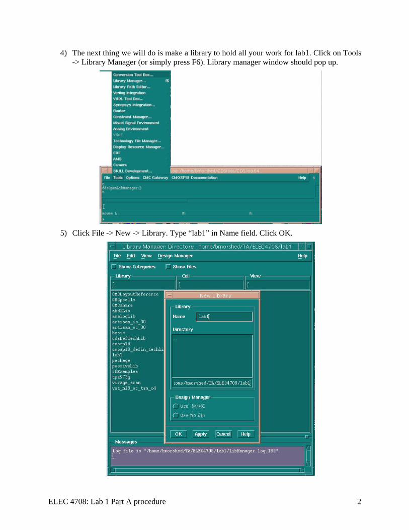
4) The next thing we will do is make a library to hold all your work for lab1. Click on Tools -> Library Manager (or simply press F6). Library manager window should pop up.
5) Click File -> New -> Library. Type “lab1” in Name field. Click OK.
ELEC 4708: Lab 1 Part A procedure 2
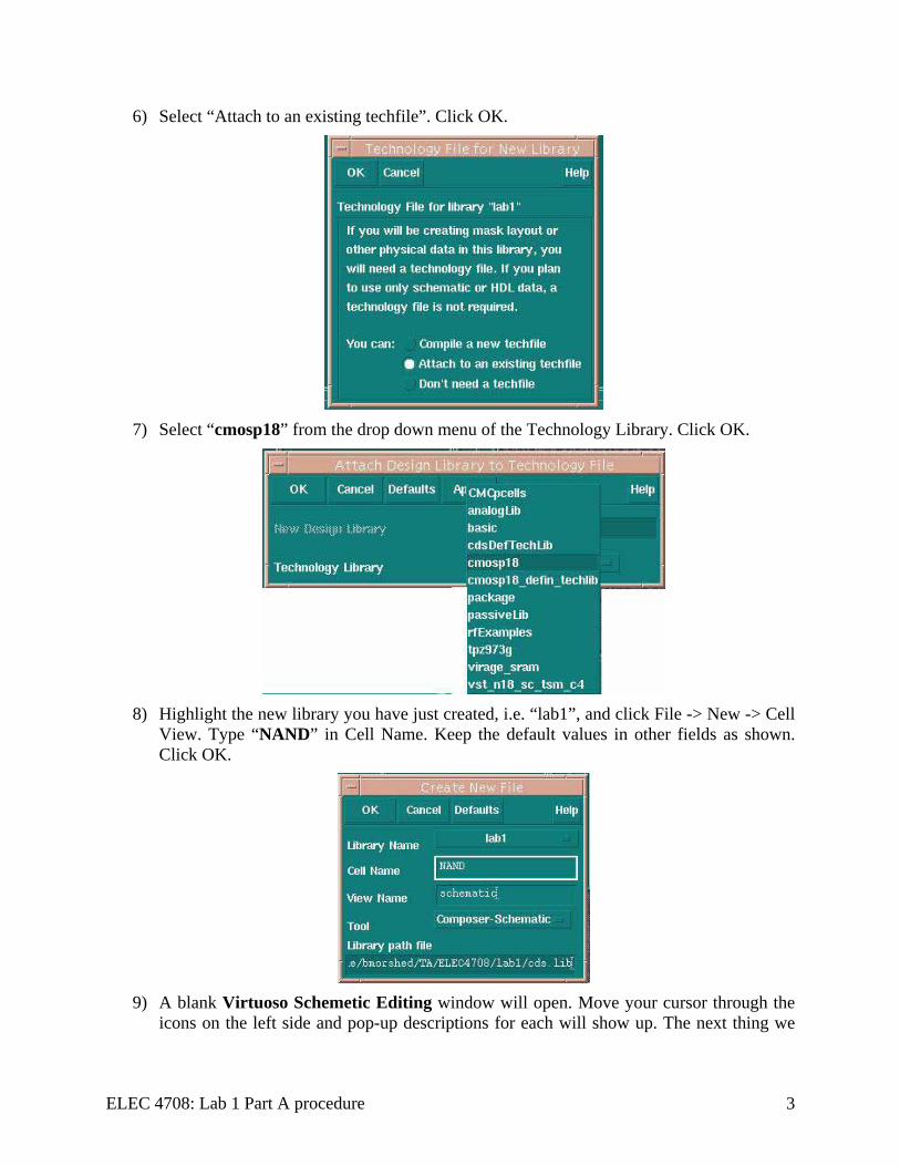
6) Select “Attach to an existing techfile”. Click OK.
7) Select “cmosp18” from the drop down menu of the Technology Library. Click OK.
8) Highlight the new library you have just created, i.e. “lab1”, and click File -> New -> Cell
View. Type “NAND” in Cell Name. Keep the default values in other fields as shown. Click OK.
9) A blank Virtuoso Schemetic Editing window will open. Move your cursor through the
icons on the left side and pop-up descriptions for each will show up. The next thing we
ELEC 4708: Lab 1 Part A procedure 3
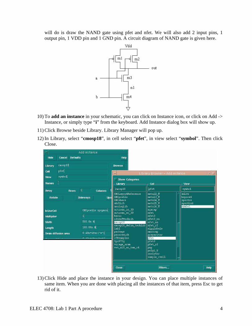
will do is draw the NAND gate using pfet and nfet. We will also add 2 input pins, 1 output pin, 1 VDD pin and 1 GND pin. A circuit diagram of NAND gate is given here.
10) To add an instance in your schematic, you can click on Instance icon, or click on Add ->
Instance, or simply type “i” from the keyboard. Add Instance dialog box will show up.
11) Click Browse beside Library. Library Manager will pop up.
12) In Library, select “cmosp18”, in cell select “pfet”, in view select “symbol”. Then click Close.
13) Click Hide and place the instance in your design. You can place multiple instances of
same item. When you are done with placing all the instances of that item, press Esc to get rid of it.
ELEC 4708: Lab 1 Part A procedure 4
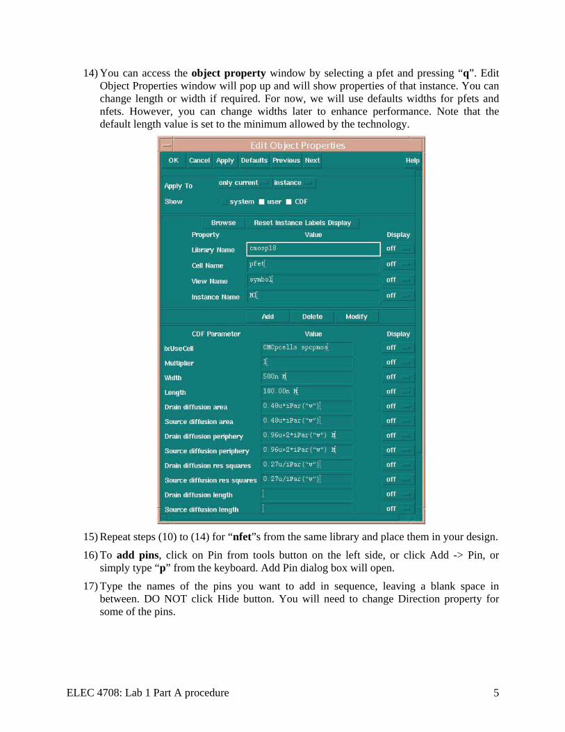
14) You can access the object property window by selecting a pfet and pressing “q”. Edit Object Properties window will pop up and will show properties of that instance. You can change length or width if required. For now, we will use defaults widths for pfets and nfets. However, you can change widths later to enhance performance. Note that the default length value is set to the minimum allowed by the technology.
15) Repeat steps (10) to (14) for “nfet”s from the same library and place them in your design.
16) To add pins, click on Pin from tools button on the left side, or click Add -> Pin, or simply type “p” from the keyboard. Add Pin dialog box will open.
17) Type the names of the pins you want to add in sequence, leaving a blank space in between. DO NOT click Hide button. You will need to change Direction property for some of the pins.
ELEC 4708: Lab 1 Part A procedure 5
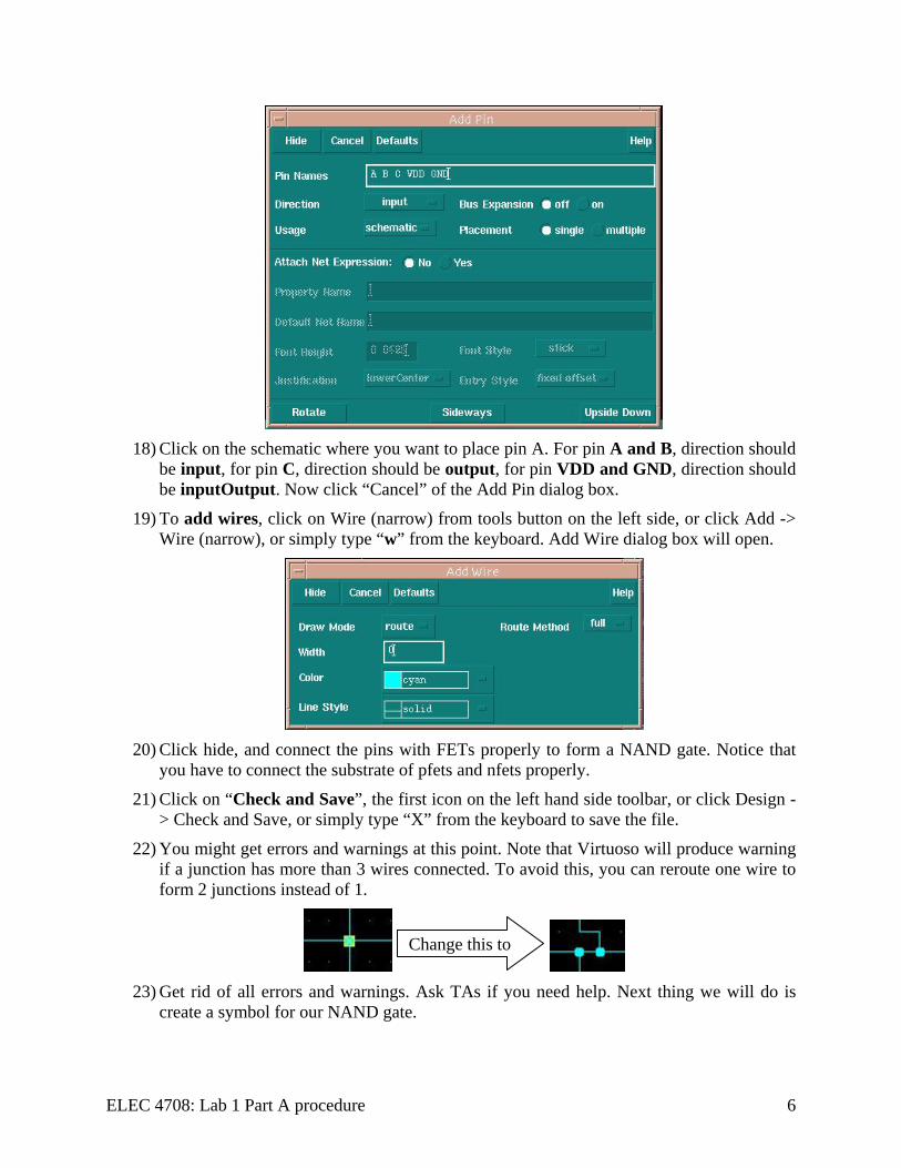
18) Click on the schematic where you want to place pin A. For pin A and B, direction should
be input, for pin C, direction should be output, for pin VDD and GND, direction should be inputOutput. Now click “Cancel” of the Add Pin dialog box.
19) To add wires, click on Wire (narrow) from tools button on the left side, or click Add -> Wire (narrow), or simply type “w” from the keyboard. Add Wire dialog box will open.
20) Click hide, and connect the pins with FETs properly to form a NAND gate. Notice that
you have to connect the substrate of pfets and nfets properly.
21) Click on “Check and Save”, the first icon on the left hand side toolbar, or click Design -> Check and Save, or simply type “X” from the keyboard to save the file.
22) You might get errors and warnings at this point. Note that Virtuoso will produce warning if a junction has more than 3 wires connected. To avoid this, you can reroute one wire to form 2 junctions instead of 1.
Change this to
23) Get rid of all errors and warnings. Ask TAs if you need help. Next thing we will do is create a symbol for our NAND gate.
ELEC 4708: Lab 1 Part A procedure 6
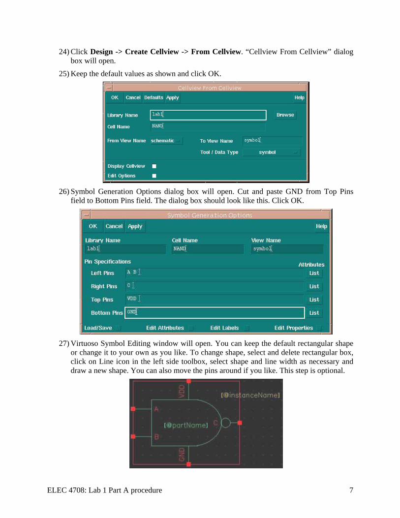
24) Click Design -> Create Cellview -> From Cellview. “Cellview From Cellview” dialog box will open.
25) Keep the default values as shown and click OK.
26) Symbol Generation Options dialog box will open. Cut and paste GND from Top Pins
field to Bottom Pins field. The dialog box should look like this. Click OK.
27) Virtuoso Symbol Editing window will open. You can keep the default rectangular shape
or change it to your own as you like. To change shape, select and delete rectangular box, click on Line icon in the left side toolbox, select shape and line width as necessary and draw a new shape. You can also move the pins around if you like. This step is optional.
ELEC 4708: Lab 1 Part A procedure 7
28) Save and close the symbol window and schematic window. You will also need to create an inverter schematic and symbol using the same procedure (step 8 to 27). Name your inverter as inv0. Next we will make a testbench to simulate our NAND gate.
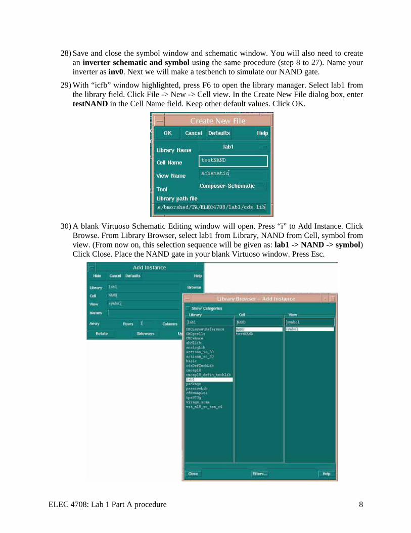
29) With “icfb” window highlighted, press F6 to open the library manager. Select lab1 from the library field. Click File -> New -> Cell view. In the Create New File dialog box, enter testNAND in the Cell Name field. Keep other default values. Click OK.
30) A blank Virtuoso Schematic Editing window will open. Press “i” to Add Instance. Click
Browse. From Library Browser, select lab1 from Library, NAND from Cell, symbol from view. (From now on, this selection sequence will be given as: lab1 -> NAND -> symbol) Click Close. Place the NAND gate in your blank Virtuoso window. Press Esc.
ELEC 4708: Lab 1 Part A procedure 8
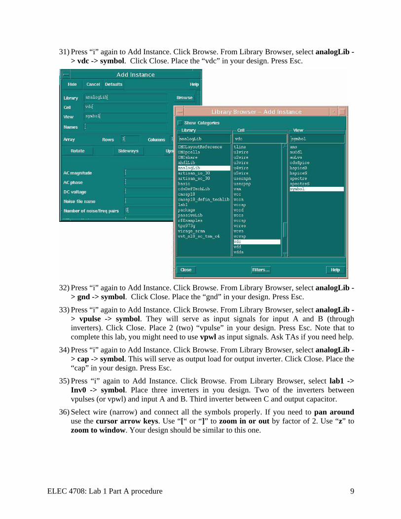
31) Press “i” again to Add Instance. Click Browse. From Library Browser, select analogLib -> vdc -> symbol. Click Close. Place the “vdc” in your design. Press Esc.
32) Press “i” again to Add Instance. Click Browse. From Library Browser, select analogLib -
> gnd -> symbol. Click Close. Place the “gnd” in your design. Press Esc.
33) Press “i” again to Add Instance. Click Browse. From Library Browser, select analogLib -> vpulse -> symbol. They will serve as input signals for input A and B (through inverters). Click Close. Place 2 (two) “vpulse” in your design. Press Esc. Note that to complete this lab, you might need to use vpwl as input signals. Ask TAs if you need help.
34) Press “i” again to Add Instance. Click Browse. From Library Browser, select analogLib -> cap -> symbol. This will serve as output load for output inverter. Click Close. Place the “cap” in your design. Press Esc.
35) Press “i” again to Add Instance. Click Browse. From Library Browser, select lab1 -> Inv0 -> symbol. Place three inverters in you design. Two of the inverters between vpulses (or vpwl) and input A and B. Third inverter between C and output capacitor.
36) Select wire (narrow) and connect all the symbols properly. If you need to pan around use the cursor arrow keys. Use “[“ or “]” to zoom in or out by factor of 2. Use “z” to zoom to window. Your design should be similar to this one.
ELEC 4708: Lab 1 Part A procedure 9
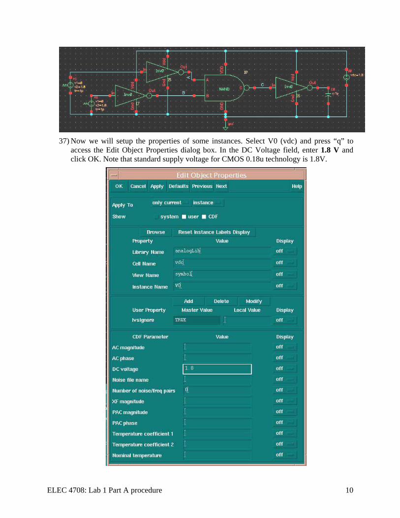
37) Now we will setup the properties of some instances. Select V0 (vdc) and press “q” to
access the Edit Object Properties dialog box. In the DC Voltage field, enter 1.8 V and click OK. Note that standard supply voltage for CMOS 0.18u technology is 1.8V.
ELEC 4708: Lab 1 Part A procedure 10
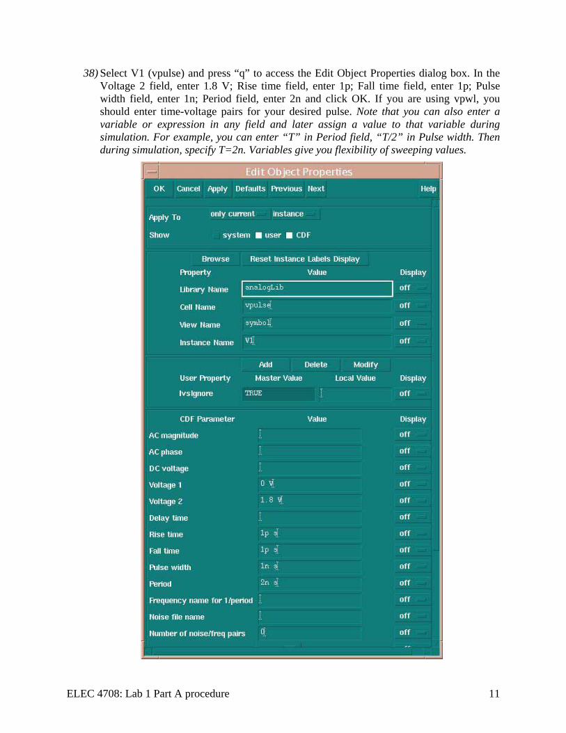
38) Select V1 (vpulse) and press “q” to access the Edit Object Properties dialog box. In the Voltage 2 field, enter 1.8 V; Rise time field, enter 1p; Fall time field, enter 1p; Pulse width field, enter 1n; Period field, enter 2n and click OK. If you are using vpwl, you should enter time-voltage pairs for your desired pulse. Note that you can also enter a variable or expression in any field and later assign a value to that variable during simulation. For example, you can enter “T” in Period field, “T/2” in Pulse width. Then during simulation, specify T=2n. Variables give you flexibility of sweeping values.
ELEC 4708: Lab 1 Part A procedure 11
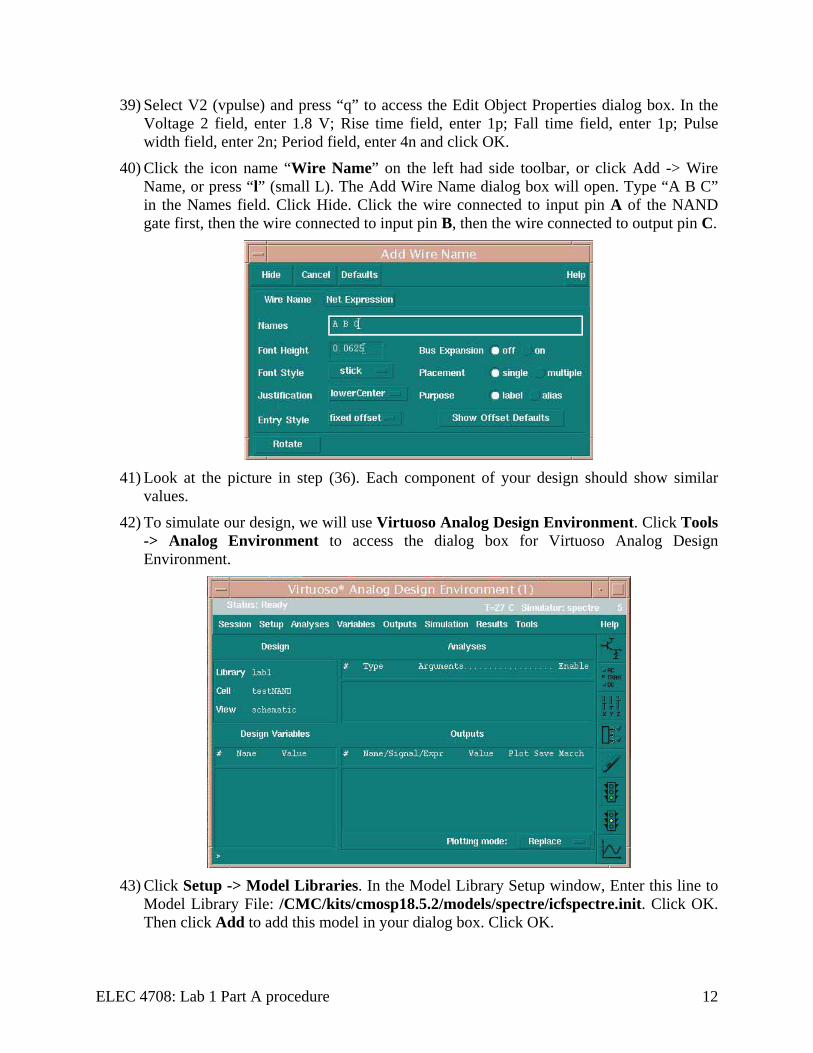
39) Select V2 (vpulse) and press “q” to access the Edit Object Properties dialog box. In the Voltage 2 field, enter 1.8 V; Rise time field, enter 1p; Fall time field, enter 1p; Pulse width field, enter 2n; Period field, enter 4n and click OK.
40) Click the icon name “Wire Name” on the left had side toolbar, or click Add -> Wire Name, or press “l” (small L). The Add Wire Name dialog box will open. Type “A B C” in the Names field. Click Hide. Click the wire connected to input pin A of the NAND gate first, then the wire connected to input pin B, then the wire connected to output pin C.
41) Look at the picture in step (36). Each component of your design should show similar
values.
42) To simulate our design, we will use Virtuoso Analog Design Environment. Click Tools -> Analog Environment to access the dialog box for Virtuoso Analog Design Environment.
43) Click Setup -> Model Libraries. In the Model Library Setup window, Enter this line to
Model Library File: /CMC/kits/cmosp18.5.2/models/spectre/icfspectre.init. Click OK. Then click Add to add this model in your dialog box. Click OK.
ELEC 4708: Lab 1 Part A procedure 12
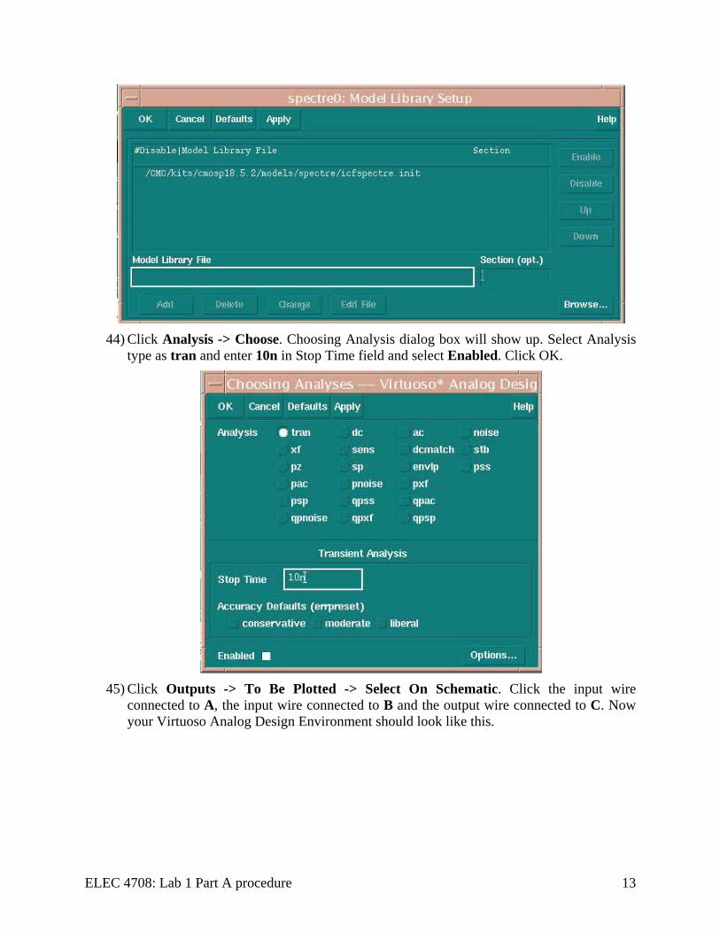
44) Click Analysis -> Choose. Choosing Analysis dialog box will show up. Select Analysis
type as tran and enter 10n in Stop Time field and select Enabled. Click OK.
45) Click Outputs -> To Be Plotted -> Select On Schematic. Click the input wire
connected to A, the input wire connected to B and the output wire connected to C. Now your Virtuoso Analog Design Environment should look like this.
ELEC 4708: Lab 1 Part A procedure 13
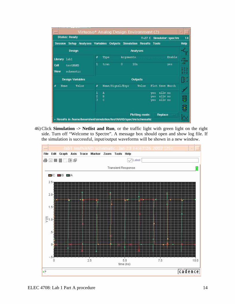
46) Click Simulation -> Netlist and Run, or the traffic light with green light on the right
side. Turn off “Welcome to Spectre”. A message box should open and show log file. If the simulation is successful, input/output waveforms will be shown in a new window.
ELEC 4708: Lab 1 Part A procedure 14
47) To see the waveform separated, select axis -> strip. To find delay manually, look at transistors of output and the corresponding input causing the transition. For example, in this case, the first output transition is at around 3 ns. To find exact value at 50% output (0.9 V), you can use Trace marker (under Marker -> Place) and click at 0.9 V crossing of the waveform. It is show the corresponding time. If you placed marker at wrong place, select that marker and click Edit -> delete.
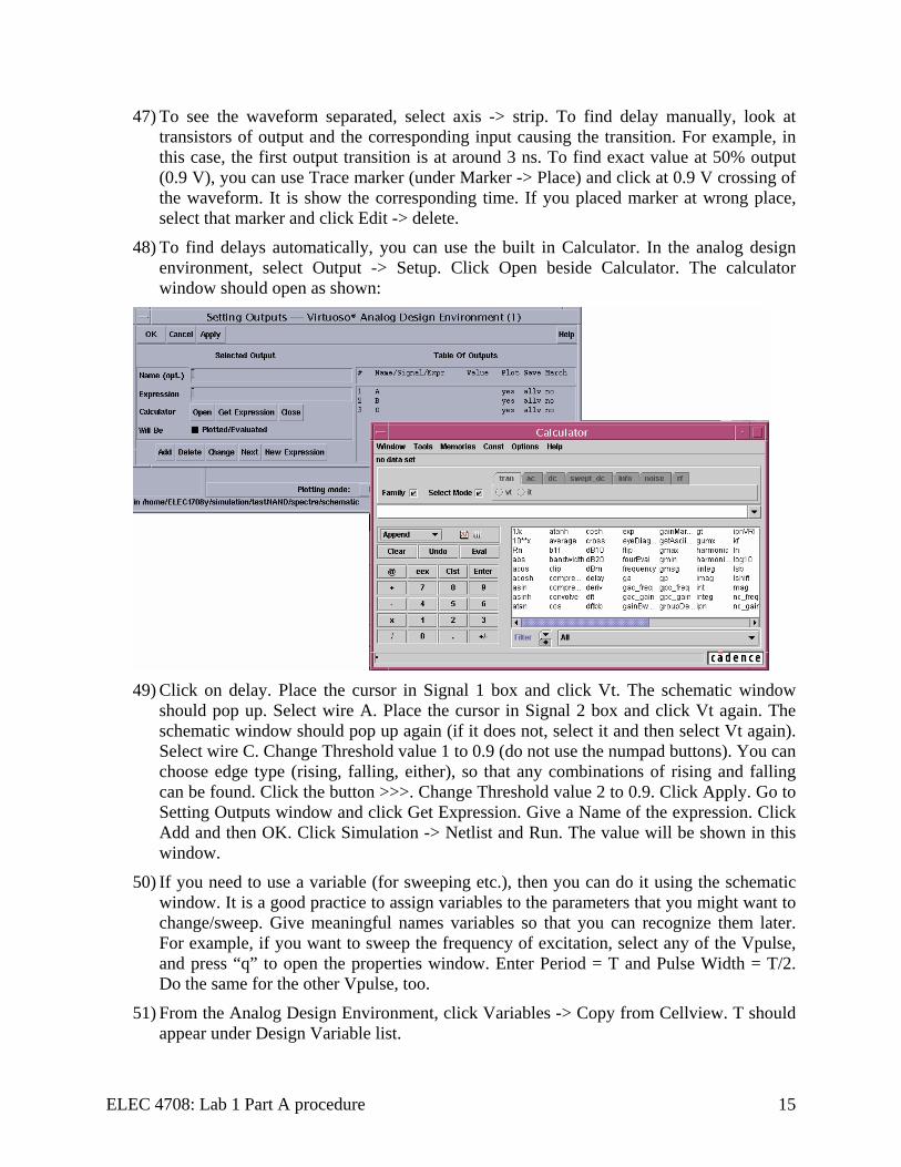
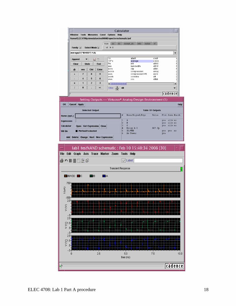
48) To find delays automatically, you can use the built in Calculator. In the analog design environment, select Output -> Setup. Click Open beside Calculator. The calculator window should open as shown:
49) Click on delay. Place the cursor in Signal 1 box and click Vt. The schematic window
should pop up. Select wire A. Place the cursor in Signal 2 box and click Vt again. The schematic window should pop up again (if it does not, select it and then select Vt again). Select wire C. Change Threshold value 1 to 0.9 (do not use the numpad buttons). You can choose edge type (rising, falling, either), so that any combinations of rising and falling can be found. Click the button >>>. Change Threshold value 2 to 0.9. Click Apply. Go to Setting Outputs window and click Get Expression. Give a Name of the expression. Click Add and then OK. Click Simulation -> Netlist and Run. The value will be shown in this window.
50) If you need to use a variable (for sweeping etc.), then you can do it using the schematic window. It is a good practice to assign variables to the parameters that you might want to change/sweep. Give meaningful names variables so that you can recognize them later. For example, if you want to sweep the frequency of excitation, select any of the Vpulse, and press “q” to open the properties window. Enter Period = T and Pulse Width = T/2. Do the same for the other Vpulse, too.
51) From the Analog Design Environment, click Variables -> Copy from Cellview. T should appear under Design Variable list.
ELEC 4708: Lab 1 Part A procedure 15
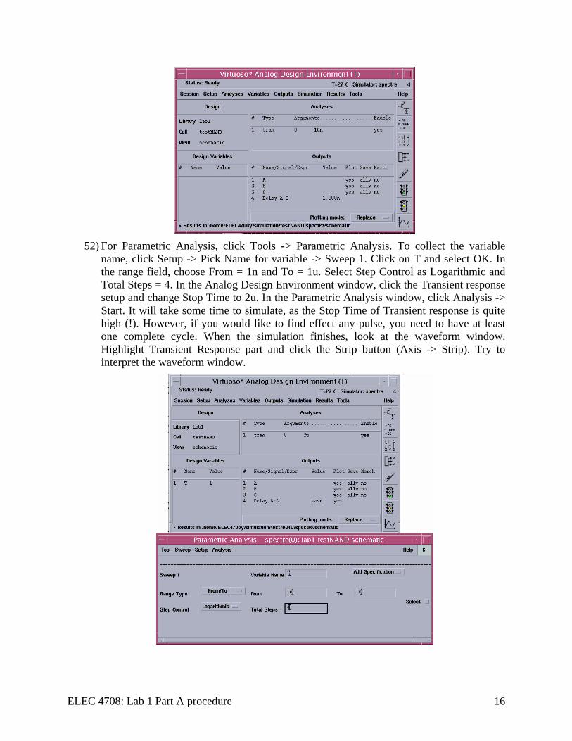
52) For Parametric Analysis, click Tools -> Parametric Analysis. To collect the variable
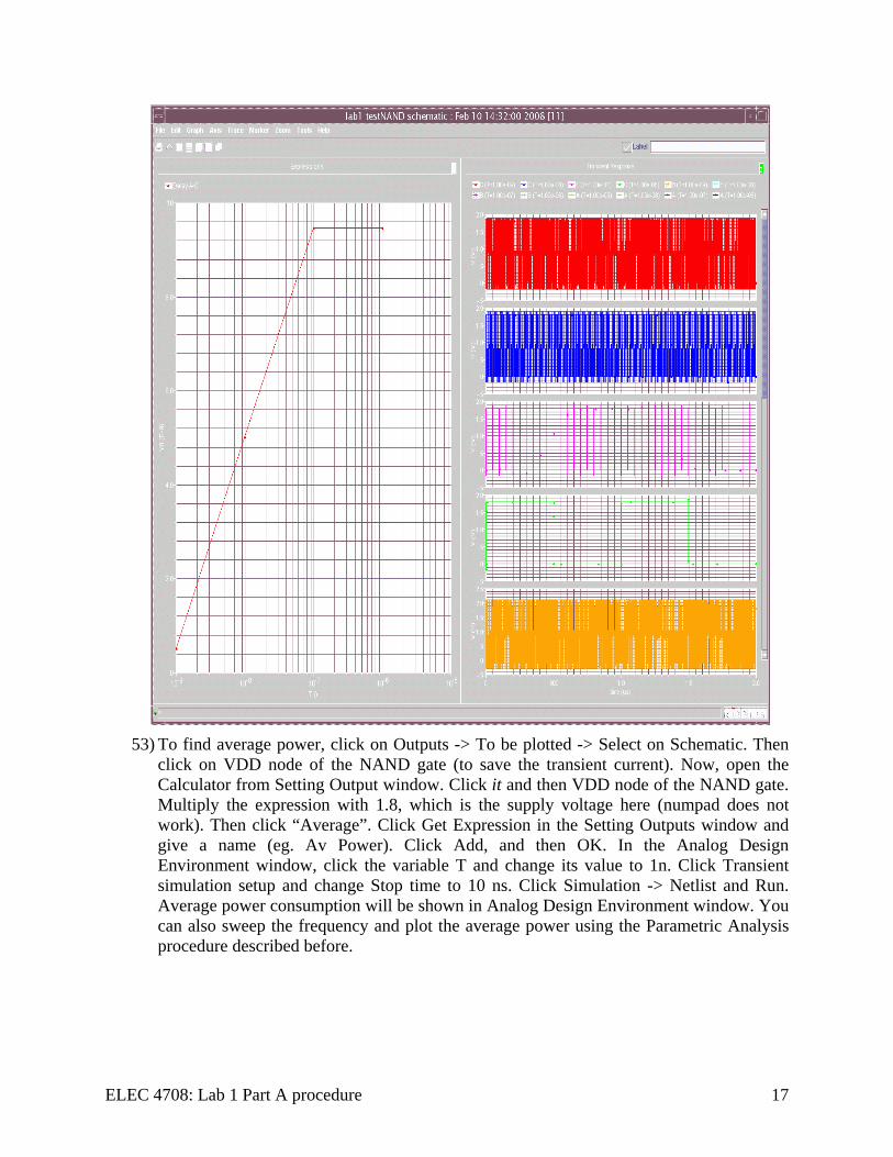
name, click Setup -> Pick Name for variable -> Sweep 1. Click on T and select OK. In the range field, choose From = 1n and To = 1u. Select Step Control as Logarithmic and Total Steps = 4. In the Analog Design Environment window, click the Transient response setup and change Stop Time to 2u. In the Parametric Analysis window, click Analysis -> Start. It will take some time to simulate, as the Stop Time of Transient response is quite high (!). However, if you would like to find effect any pulse, you need to have at least one complete cycle. When the simulation finishes, look at the waveform window. Highlight Transient Response part and click the Strip button (Axis -> Strip). Try to interpret the waveform window.
ELEC 4708: Lab 1 Part A procedure 16
53) To find average power, click on Outputs -> To be plotted -> Select on Schematic. Then
click on VDD node of the NAND gate (to save the transient current). Now, open the Calculator from Setting Output window. Click it and then VDD node of the NAND gate. Multiply the expression with 1.8, which is the supply voltage here (numpad does not work). Then click “Average”. Click Get Expression in the Setting Outputs window and give a name (eg. Av Power). Click Add, and then OK. In the Analog Design Environment window, click the variable T and change its value to 1n. Click Transient simulation setup and change Stop time to 10 ns. Click Simulation -> Netlist and Run. Average power consumption will be shown in Analog Design Environment window. You can also sweep the frequency and plot the average power using the Parametric Analysis procedure described before.
ELEC 4708: Lab 1 Part A procedure 17
ELEC 4708: Lab 1 Part A procedure 18
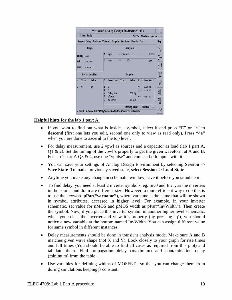
Helpful hints for the lab 1 part A:
• If you want to find out what is inside a symbol, select it and press “E” or “e” to descend (first one lets you edit, second one only to view as read only). Press “^e” when you are done to ascend to the top level.
• For delay measurement, use 2 vpwl as sources and a capacitor as load (lab 1 part A, Q1 & 2). Set the timing of the vpwl’s properly to get the given waveform at A and B. For lab 1 part A Q3 & 4, use one “vpulse” and connect both inputs with it.
• You can save your settings of Analog Design Environment by selecting Session -> Save State. To load a previously saved state, select Session -> Load State.
• Anytime you make any change in schematic window, save it before you simulate it.
• To find delay, you need at least 2 inverter symbols, eg. Inv0 and Inv1, as the inverters in the source and drain are different size. However, a more efficient way to do this is to use the keyword pPar(“varname”), where varname is the name that will be shown in symbol attributes, accessed in higher level. For example, in your inverter schematic, set value for nMOS and pMOS width as pPar(“InvWidth”). Then create the symbol. Now, if you place this inverter symbol in another higher level schematic, when you select the inverter and view it’s property (by pressing ‘q’), you should notice a new variable at the bottom named InvWidth. You can assign different value for same symbol in different instances.
• Delay measurements should be done in transient analysis mode. Make sure A and B matches given wave shape (not X and Y). Look closely to your graph for rise times and fall times (You should be able to find all cases as required from this plot) and tabulate them. Find propagation delay (maximum) and contamination delay (minimum) from the table.
• Use variables for defining widths of MOSFETs, so that you can change them from during simulations keeping β constant.
ELEC 4708: Lab 1 Part A procedure 19