Embed Size (px)
Citation preview


1
§ CONTENTS
SPECIFICATIONS ---------------------------------------------------------------- 2
SAFETY INSTRUCTIONS °¶°¶°¶°¶°¶°¶°¶°¶°¶°¶°¶°¶°¶°¶°¶°¶°¶°¶°¶°¶°¶°¶°¶°¶°¶°¶°¶°¶ 3
BLOCK DIAGRAM°¶°¶°¶°¶°¶°¶°¶°¶°¶°¶°¶°¶°¶°¶°¶°¶°¶°¶°¶°¶°¶°¶°¶°¶°¶°¶°¶°¶°¶°¶°¶°¶ 4
GENERAL ALIGNMENT INSTRUCTIONS °¶°¶°¶°¶°¶°¶°¶°¶°¶°¶°¶°¶°¶°¶°¶°¶°¶°¶°¶°¶°¶ 6
DESCRIPTION OF THE CIRCUIT OPERATION °¶°¶°¶°¶°¶°¶°¶°¶°¶°¶°¶°¶°¶°¶°¶°¶°¶°¶ 10
TROUBLE SHOOTING CHARTS °¶°¶°¶°¶°¶°¶°¶°¶°¶°¶°¶°¶°¶°¶°¶°¶°¶°¶°¶°¶°¶°¶°¶°¶°¶ 32
PRINTED CIRCUIT BOARDS °¶°¶°¶°¶°¶°¶°¶°¶°¶°¶°¶°¶°¶°¶°¶°¶°¶°¶°¶°¶°¶°¶°¶°¶°¶°¶ 40
REPLACEMENT PARTS LIST °¶°¶°¶°¶°¶°¶°¶°¶°¶°¶°¶°¶°¶°¶°¶°¶°¶°¶°¶°¶°¶°¶°¶°¶°¶°¶ 41
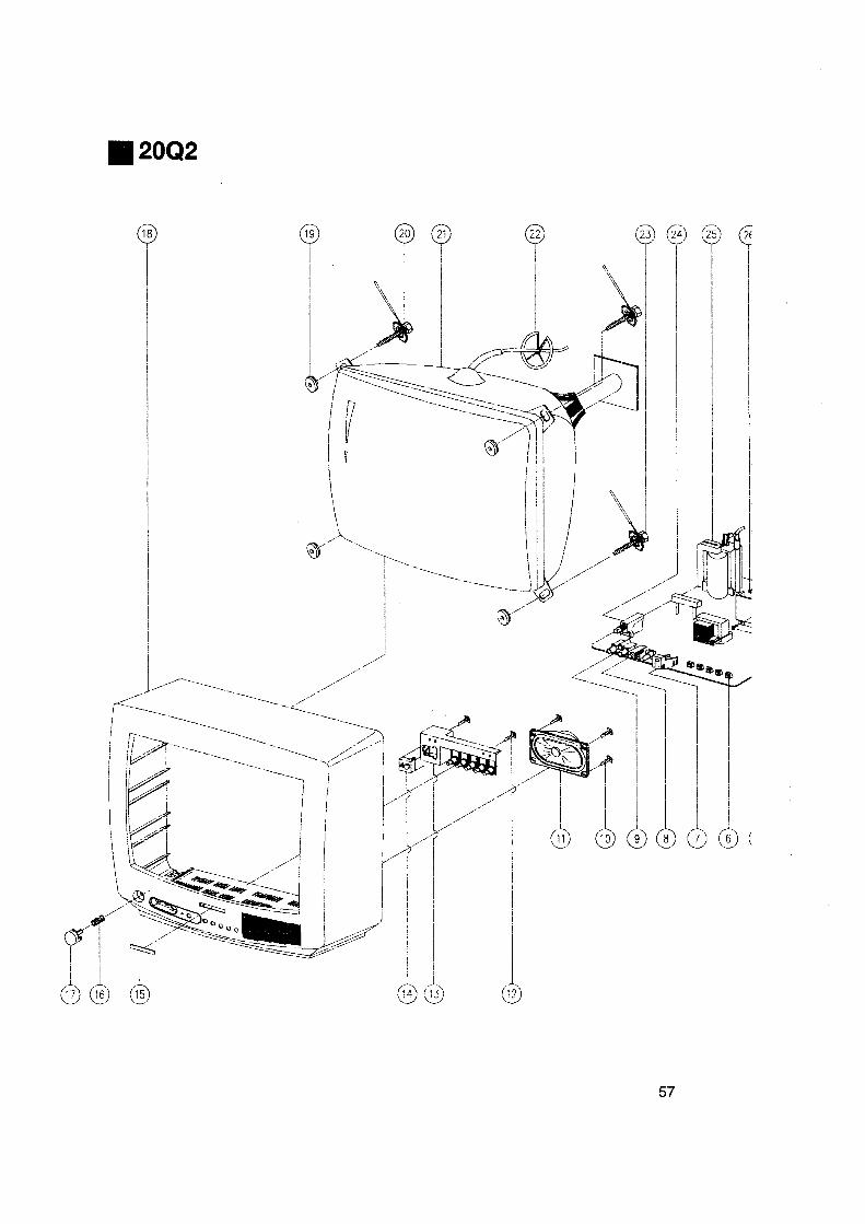
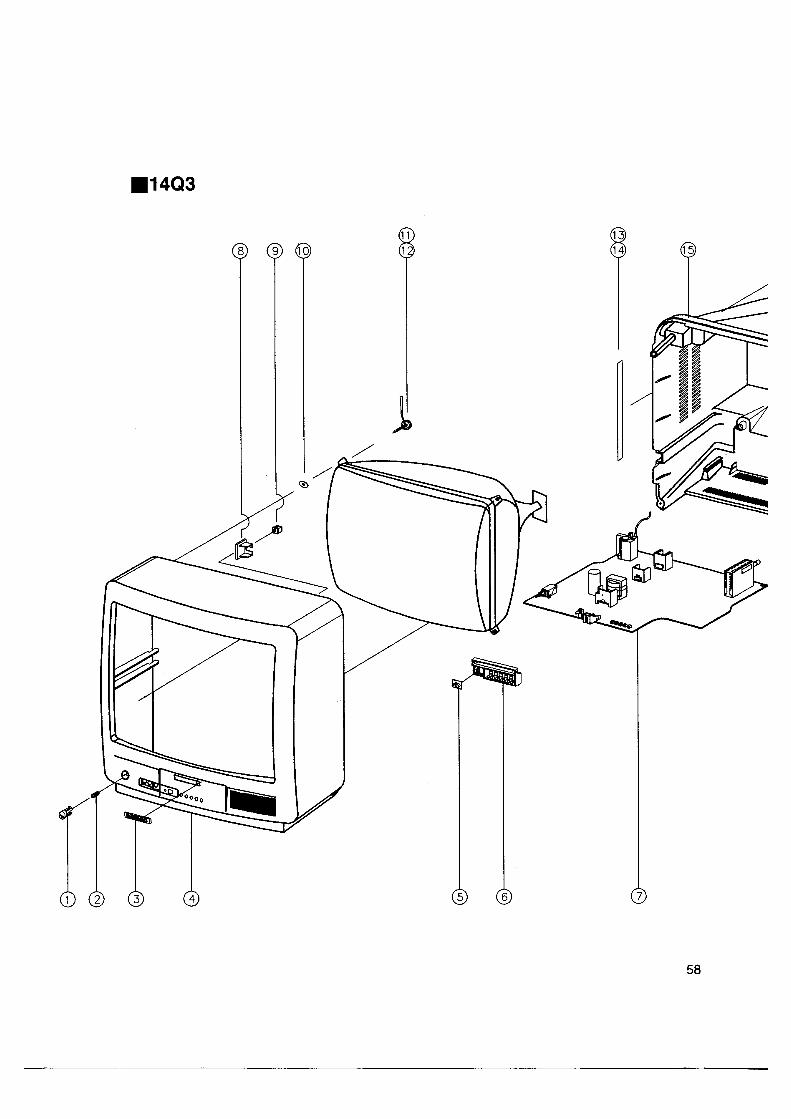
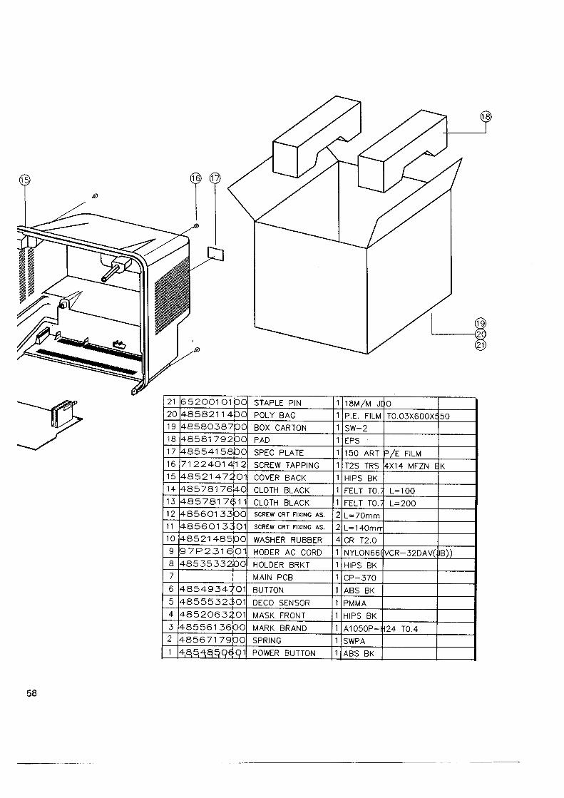
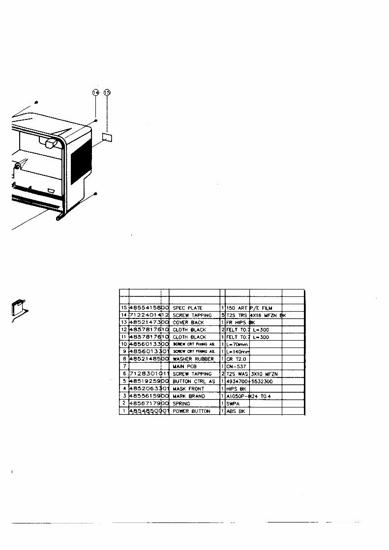
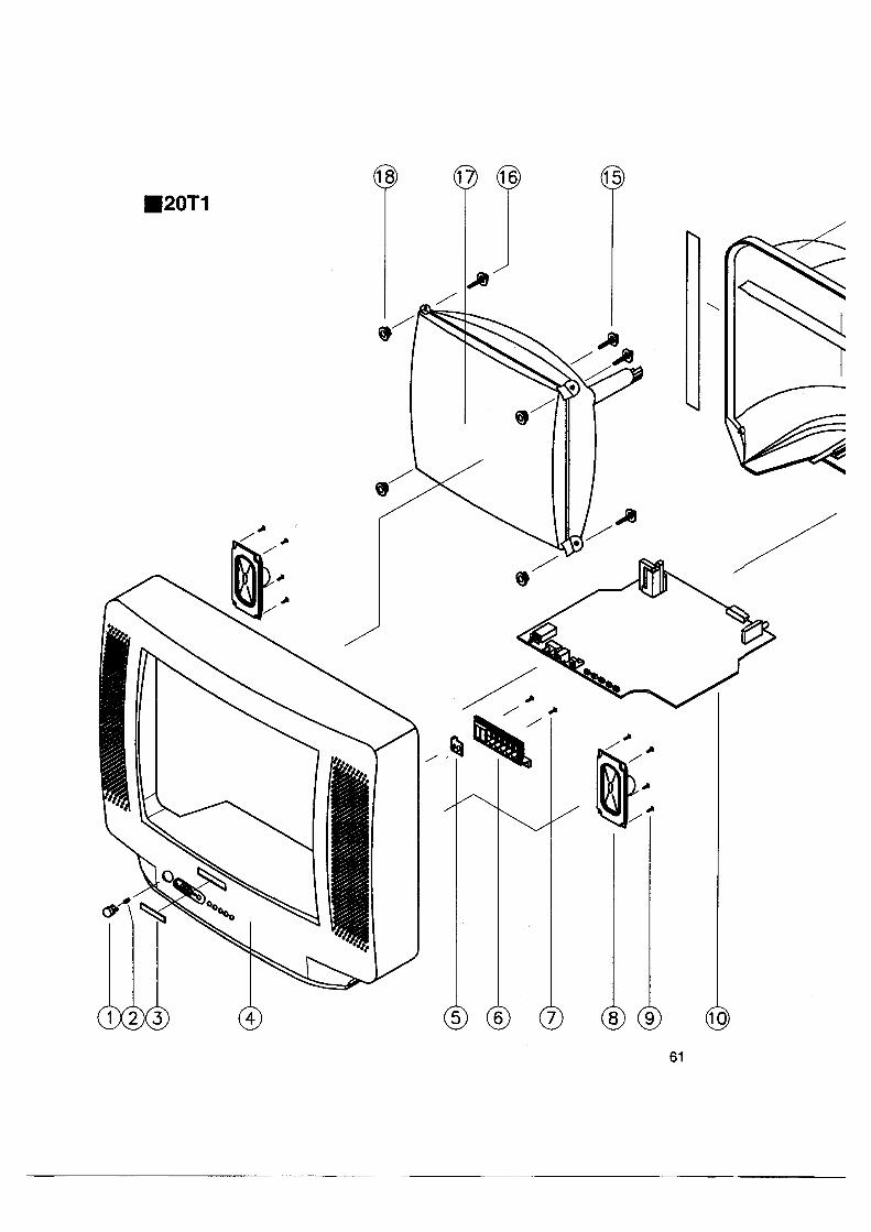
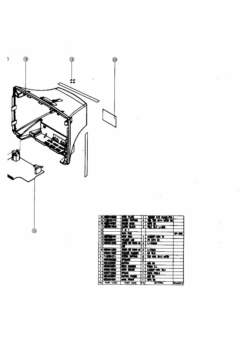
EXPLODED VIEW °¶°¶°¶°¶°¶°¶°¶°¶°¶°¶°¶°¶°¶°¶°¶°¶°¶°¶°¶°¶°¶°¶°¶°¶°¶°¶°¶°¶°¶°¶°¶ 54
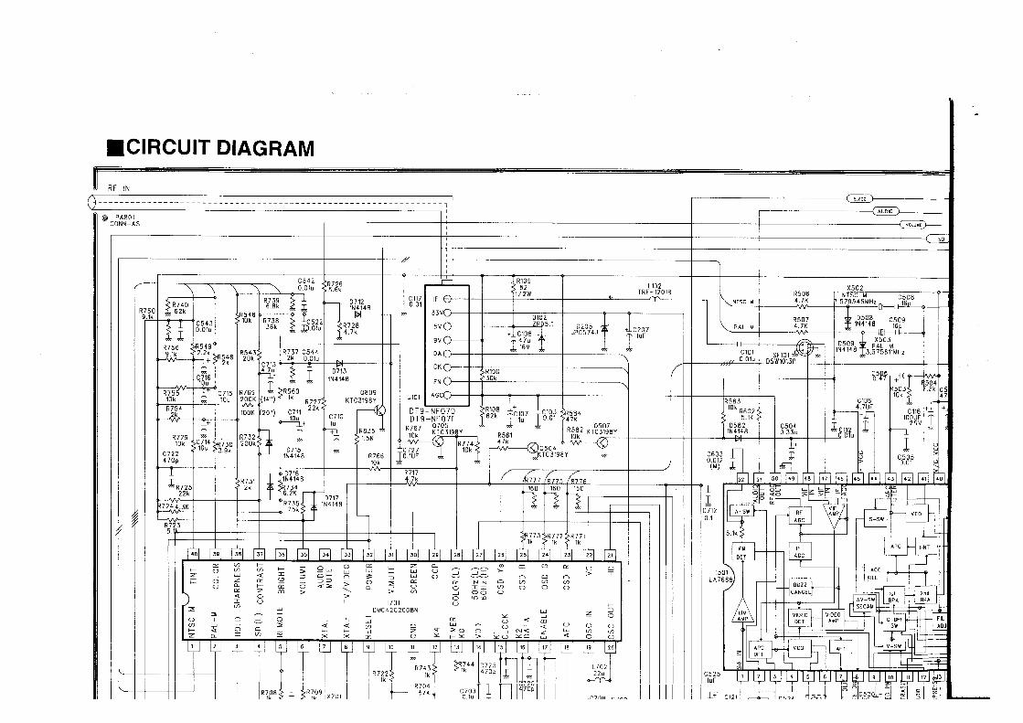
CIRCUIT DIAGRAM°¶°¶°¶°¶°¶°¶°¶°¶°¶°¶°¶°¶°¶°¶°¶°¶°¶°¶°¶°¶°¶°¶°¶°¶°¶°¶°¶°¶°¶°¶°¶ 64

2
CHASSIS CM-537
Receiving System NTSC/PAL-M/PAL-N
Main Voltage AC 100/220V, 50/60Hz
Power Consumption 60 Watts (14”) / 65 Watts (20”)
Sound Output 2.5W (16§ )
Antenna Impedance 75§ Unbalanced
Tuning System Frequency Synthesizer
Number of Memory 181 Channels
Channel
Reception Channel VHF TV LOW:CH2~6
HIGH:CH7~13
UHF TV CH14~CH69
CATV CH1~CH125
Remote Control Unit R-25C04
Screen Size 14” / 20”(diagonal)
Color Standard NTSC/PAL-N,M
Tuner Type Varactor Type with PLL
Aux. Terminal Input:Video,Audio
§ SPECIFICATIONS

3
§ SAFETY INSTRUCTIONS
10WATTGood earth ground,such as the waterpipe, conduit, etc.
1500 OHM
0.15MFD
AC VOLT METER
Place this probeon each exposedmetallic part.
Many electrical and mechanical parts in this chassis have specialsafety-related characteristics. These characterictics are oftenpassed unnoticed by a visual inspection and the protectionafforded by them cannot necessarily be obtained by usingreplacement components rated for higher volage, wattage,etc.Replacement parts which have these special safetycharacteristics are identif ied in this manual and its
supplements;electrical components having such features areidentified by shading on the schematic diagram and the parts list.Before replacing any of these components, read the parts list inthis manual carefully. The use of substitute replacement partswhich do not have the same safety characteristics as specified inthe parts list may create shock, fire or other hazards.
§ PRODUCT SAFETY NOTICE
WARNING: Service should not be attempted by anyone unfamiliarwith the necessary precaution on this receiver.The following are the necessary precaution to be observed beforeservicing.1.Always discharge the picture tube anode to the CRT conductive
coating the picture tube. the picture tube is hightly evacuatedand if broken, glass fragments will be violently expelled. Useshatterproofgoggles and keep picture tube away from the bodywhile handling.
2.When replacing chassis in the cabinet,always be certain that allthe protective devices are put back in place, such as;nonmetallic control knobs, insulating covers, shields, isolationresistor-capacitor network, etc
3.Before retuning the set to the customer, always perform an ACleakage current check on the exposed metallic parts of thecabinet, such as antennas, terminals, screwheads, metaloverlays, control shafts etc, to be sure the set is safe to operatewithout danger of electrical shock.
Plug the AC line cord directly into a AC outlet. Use an ACvoltmeter having 500 ohms per volt or more sensitivily in thefollowing manner.Connect a 1500 ohm 10 watt resistor, paralleled by a 0.15 mfd,AC type capacitor, between a known good earth ground( waterpipe, conduit etc) and the exposed metallic parts, one at a time.Measure the AC voltage across the combination of 1500 ohmresistor and 0.15 mfd capacitor.Reverse the ac plug at the ac outlet and repeat AC voltagemeasurements for each exposed metallic part. Voltage measuredmust not exceed 0.3 volts RMS. This corresponds to 0.2 milliamp,AC. Any value exceeding this limit constitutes a potential shockhazard and must be corrected immediately.
§ SAFETY PRECAUTION
§ SERVICE NOTES
1.When replacing parts or circuit boards, clamp the lead wires toterminal before soldering.
2.When replacing a high wattage resistor(metal oxide filmresistor)in the circuit board keep the resistor min 1/2 inch awayfrom the circuit board.
3.Keep wires away form high voltage or high temperaturecomponents.

5
§ LOCATION OF CONTROLS
§ REMOTE CONTROL UNIT
MAIN POWER VIDEO AUDIO STAND-BY C H VOL MENU
1 2 3
4 5 6
7 8 9
0
REMOTE CONTROLLER R-25C
POWER
CH¡ª
MENU
CH¡
VOL¢‚
VOL¢”
RECALL MUTEADD/ERA
SLEEP PREV.CH
TV/VIDEO AIR/CABLEAUTO.PICT
2
2
3 3
1
7
10
12
3
56
8
9
1311
1. POWERUsed to turn TV ON or OFF.
2. ¡¡ªªCH¡¡ÂUse these buttons to change channels on yourTV, or select items in the menu system.
3. ¢¢‚‚VOL¢¢””Use these buttons to change your TV’svolume, to activate selections in the menusystem, or to change audio and video settings.
4. MENUUse this button to turn TV’s menu systemon and off.
5. RECALLPress this button to display the channelnumber
6. ADD/ERAUse this button to add a channel to the TV’smemory or erase the channel from memory.
7. MUTEUse to turn the TV’s sound on and off.
8. 0-9Use these buttons to change channels.
9. SLEEPUse this button to program the TV to turn offafter a certain time.
10. PREV.CHPress this button to return to the previouschannel you were watching.
11. AUTO.PICT.Press this button to return TV’s video settings to their original level.
12. AIR/CABLEUse the button to set up your TV to receivesignals from an antenna (AIR) or a cablesystem (CABLE)
13. TV/VIDEOUse the button to seiect TV or VIDEO mode.

6
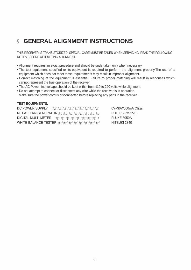
§ GENERAL ALIGNMENT INSTRUCTIONS
THIS RECEIVER IS TRANSISTORIZED. SPECIAL CARE MUST BE TAKEN WHEN SERVICING. READ THE FOLLOWINGNOTES BEFORE ATTEMPTING ALIGNMENT.
• Alignment requires an exact procedure and should be undertaken only when necessary.• The test equipment specified or its equivalent is required to perform the alignment properly.The use of a
equipment which does not meet these requirements may result in improper alignment.• Correct matching of the equipment is essential. Failure to proper matching will result in responses which
cannot represent the true operation of the receiver.• The AC Power line voltage should be kept within from 110 to 220 volts while alignment.• Do not attempt to connect or disconnect any wire while the receiver is in operation.Make sure the power cord is disconnected before replacing any parts in the receiver.
TEST EQUIPMENTS.DC POWER SUPPLY ¡ƒ¡ƒ¡ƒ¡ƒ¡ƒ¡ƒ¡ƒ¡ƒ¡ƒ¡ƒ¡ƒ¡ƒ¡ƒ¡ƒ¡ƒ¡ƒ¡ƒ¡ƒ¡ƒ 0V~30V/500mA Class.RF PATTERN GENERATOR¡ƒ¡ƒ¡ƒ¡ƒ¡ƒ¡ƒ¡ƒ¡ƒ¡ƒ¡ƒ¡ƒ¡ƒ¡ƒ¡ƒ¡ƒ¡ƒ¡ƒ PHILIPS PM-5518DIGITAL MULTI METER ¡ƒ¡ƒ¡ƒ¡ƒ¡ƒ¡ƒ¡ƒ¡ƒ¡ƒ¡ƒ¡ƒ¡ƒ¡ƒ¡ƒ¡ƒ¡ƒ¡ƒ¡ƒ FLUKE 8050AWHITE BALANCE TESTER ¡ƒ¡ƒ¡ƒ¡ƒ¡ƒ¡ƒ¡ƒ¡ƒ¡ƒ¡ƒ¡ƒ¡ƒ¡ƒ¡ƒ¡ƒ¡ƒ¡ƒ NITSUKI 2840

7
§ PIF VCO ADJUSTMENT[Measuring Instrument Connection]
1. Connect the 12V DC POWER SUPPLY to TP4 and TP5.2. Set the frequency of RF PATTERN GENERATOR with COLOR BAR PATTERN signal to 45.75MHz,
and connect the RF output to TP1.3. Connect the DIGITAL MULTI METER to TP3.4. Adjust L506 so that the voltage of TP3 becomes 3.8V ± 0.1 Vdc within two DROP-POINTs (FIGURE 2).
§ SCREEN ADJUSTMENT
1. Push the 9D.SCR key of SERVICE REMOCON to obtain one line picture of screen.2. Adjust the R,G,B Bias volume in order that the one line of screen may become white color.
RF PATTERNGENERATORPM-5518
DIGITAL MULTIMETER
DC POWERSUPPLY
TP1(L102)
TP3(I501 #7)
TP4(R701)
TP5(I201)
[ADJUSTMENT SET]
(FIGURE 1)
(FIGURE 2)
adjust point
core(L506) rotating
voltage drop points
V
3.8V

8
3. Adjust the SCREEN VOLUME of FBT in order that the one line of screen disappear.4. Push the 9D.SCR key of SERVICE REMOCON again.
§ FOCUS ADJUSTMENT
1. Receive the RETMA pattern.2. Adjust the FOCUS volume of FBT to obtain the most clear picture.
§ RF AGC ADJUSTMENT
1. Input the COLOR BAR SIGNAL of 65dB to the ANTENNA INPUT of TV SET2. Set the user control to AUTO PICTURE ON.3. Turn completely the RF AGC volume R101 counter-clockwise and turn it clockwise until AGC voltage 6.0V is
obtained.4. If there is the BEAT with strong signal(95 dB over), re-adjust it.
§ VERTICAL CENTER ADJUSTMENT
1. Receive the RETMA PATTERN.3. Set the user control to AUTO PICTURE ON.4. Adjust the R302 so that the horizontal center of the PATTERN may meet with the mechanical center of CRT.
§ HORIZONTAL CENTER ADJUSTMENT
1.Receive the RETMA PATTERN.2.Set the user control to AUTO PICTURE ON.3. Adjust the R501 in order that the circle may put in the center position of the screen.
41
14
14
41
5 3 1 1 3 5
(FIGURE 3) VERTICAL and HORIZONTAL center Adjustmemt
9
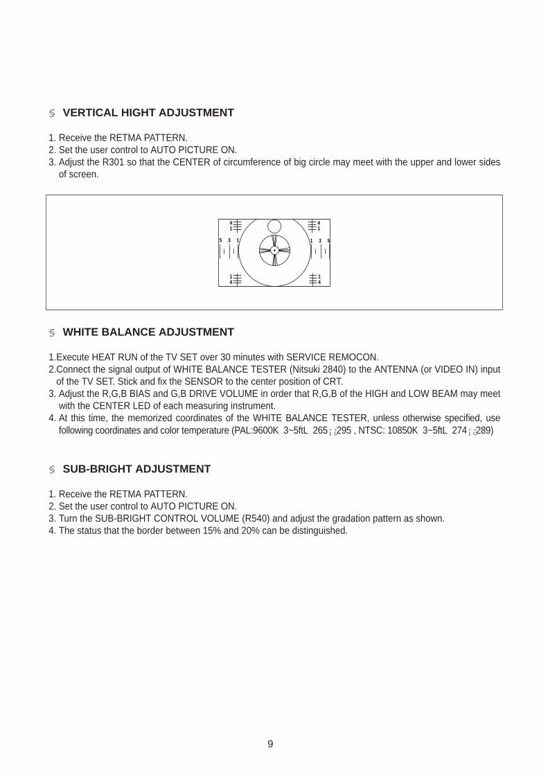
§ VERTICAL HIGHT ADJUSTMENT
1. Receive the RETMA PATTERN.2. Set the user control to AUTO PICTURE ON.3. Adjust the R301 so that the CENTER of circumference of big circle may meet with the upper and lower sides
of screen.
§ WHITE BALANCE ADJUSTMENT
1.Execute HEAT RUN of the TV SET over 30 minutes with SERVICE REMOCON.2.Connect the signal output of WHITE BALANCE TESTER (Nitsuki 2840) to the ANTENNA (or VIDEO IN) input
of the TV SET. Stick and fix the SENSOR to the center position of CRT.3. Adjust the R,G,B BIAS and G,B DRIVE VOLUME in order that R,G,B of the HIGH and LOW BEAM may meet
with the CENTER LED of each measuring instrument.4. At this time, the memorized coordinates of the WHITE BALANCE TESTER, unless otherwise specified, use
following coordinates and color temperature (PAL:9600K 3~5ftL 265¡¿295 , NTSC: 10850K 3~5ftL 274¡¿289)
§ SUB-BRIGHT ADJUSTMENT
1. Receive the RETMA PATTERN.2. Set the user control to AUTO PICTURE ON.3. Turn the SUB-BRIGHT CONTROL VOLUME (R540) and adjust the gradation pattern as shown.4. The status that the border between 15% and 20% can be distinguished.
41
14
14
41
5 3 1 1 3 5

10
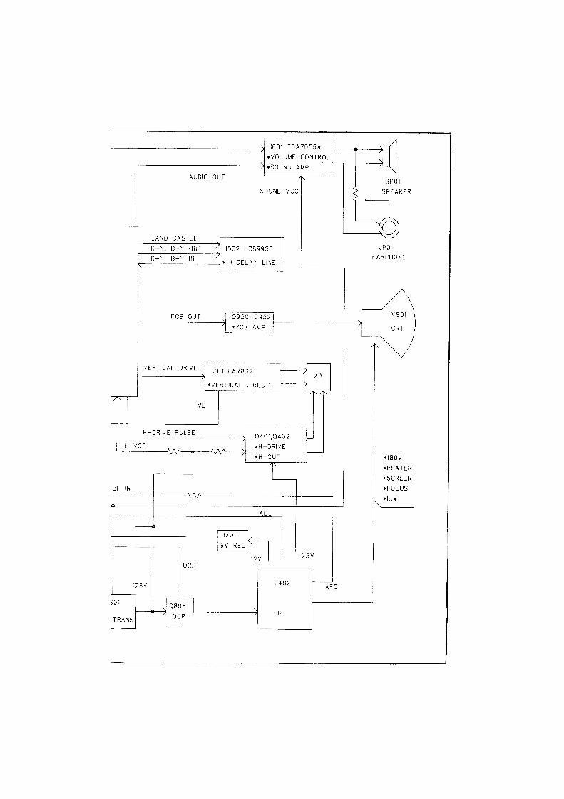
§ DESCRIPTION OF CIRCUIT OPERATION
§ FEATURE OF THE CM-537•VIDEO, CHROMA, DEFLECTION in one-chip IC.•Automatic switching of 3-SYSTEM(NTSC, PAL-M, PAL-N).•FS(Frequency Synthesizer ) Tunning System.•Function of LAST MEMORY against the electric failure (E2PROM:24LC028).•Separation of PIF and SIF(SAW filter :DSW1013P)•Minimization of Ringing by applying Ringing-less FBT(2001SPND)•Auto-compensation of the vertical height level against the frequency change of AC power .•OVER CURRENT PROTECTION Circuit.•Elimination Circuit of POP NOISE.
§ OPERATION CHARACTERISTICS OF EACH BLOCK
A.¥-COM BLOCK1. ¥-COM(DMC42C522N, I701) PIN DESCRIPTION/OPERATION
PIN NAME/(ABBREV) FUNCTION REMARK
1 NTSC-M 3-SYSTEM SWITCHING CMOS(RCO/PWM14) PUSH PULL
2 PAL-M 3-SYSTEM SWITCHING CMOS(R83) PUSH PULL
3 AC POWER DOWN MAIN POWER DOWN Detect input:active LOW CMOS(R03/INT3) PUSH PULL
4 SD INPUT SYNC. signal INPUT H: signal detect(RO2/INT2) L: no signal
5 REMOTE CONTROL REMOTE CONTROL signal inputINPUT REMOTE CONTROL IC : M50560-388GP/M50560-001(R01/INT1TIM1) (CUSTOM CODE: 14H)
6 KEY RETURN IN 0 ·KEY MATRIX COLUMN 0(R00/INT0/TIM0) ·HOLD MODE : WAKE-UP using INT1 PUSH PULL
7 Xin SYSTEM CLOCK : 4.1943 MHz8 Xout9 RESET SYSTEM RESET10 KEY RETURN IN 1 KEY MATRIX COLUMN 1
(R82)11 Vss GND12 KEY RETURN IN 2 KEY MATRIX COLUMN 2
(R81)13 KEY SCAN OUT 0 · KEY MATRIX ROW 0
& TIMER · Active HIGH when ON TIMER is set.(R80)
11
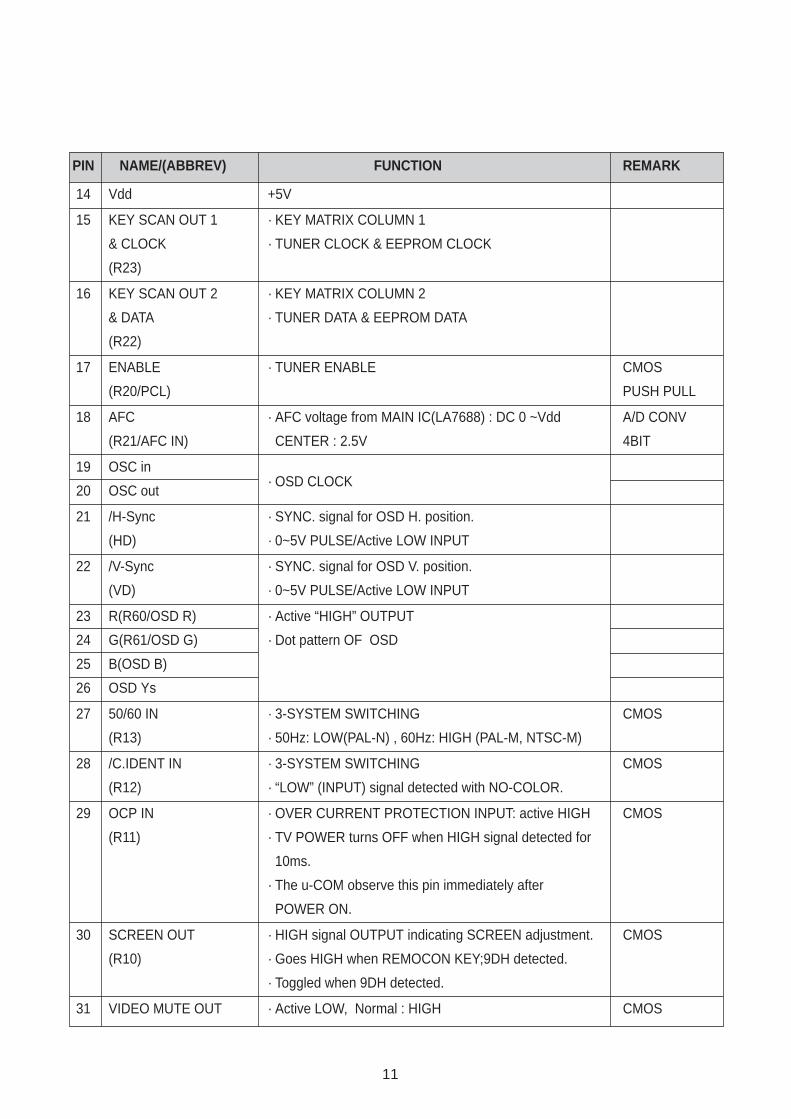
PIN NAME/(ABBREV) FUNCTION REMARK
14 Vdd +5V
15 KEY SCAN OUT 1 · KEY MATRIX COLUMN 1
& CLOCK · TUNER CLOCK & EEPROM CLOCK
(R23)
16 KEY SCAN OUT 2 · KEY MATRIX COLUMN 2
& DATA · TUNER DATA & EEPROM DATA
(R22)
17 ENABLE · TUNER ENABLE CMOS
(R20/PCL) PUSH PULL
18 AFC · AFC voltage from MAIN IC(LA7688) : DC 0 ~Vdd A/D CONV
(R21/AFC IN) CENTER : 2.5V 4BIT
19 OSC in· OSD CLOCK
20 OSC out
21 /H-Sync · SYNC. signal for OSD H. position.
(HD) · 0~5V PULSE/Active LOW INPUT
22 /V-Sync · SYNC. signal for OSD V. position.
(VD) · 0~5V PULSE/Active LOW INPUT
23 R(R60/OSD R) · Active “HIGH” OUTPUT
24 G(R61/OSD G) · Dot pattern OF OSD
25 B(OSD B)
26 OSD Ys
27 50/60 IN · 3-SYSTEM SWITCHING CMOS
(R13) · 50Hz: LOW(PAL-N) , 60Hz: HIGH (PAL-M, NTSC-M)
28 /C.IDENT IN · 3-SYSTEM SWITCHING CMOS
(R12) · “LOW” (INPUT) signal detected with NO-COLOR.
29 OCP IN · OVER CURRENT PROTECTION INPUT: active HIGH CMOS
(R11) · TV POWER turns OFF when HIGH signal detected for
10ms.
· The u-COM observe this pin immediately after
POWER ON.
30 SCREEN OUT · HIGH signal OUTPUT indicating SCREEN adjustment. CMOS
(R10) · Goes HIGH when REMOCON KEY;9DH detected.
· Toggled when 9DH detected.
31 VIDEO MUTE OUT · Active LOW, Normal : HIGH CMOS

12
PIN NAME/(ABBREV) FUNCTION REMARK
32 POWER · Active HIGH· LOW state at initial condition (RESET). except· Toggle LOW/HIGH when POWER KEY input is detected. HEAT-RUN mode
(LOW ¡ POWER OFF / HIGH ¡ POWER ON)· Automatically turns to LOW when SLEEP TIMER
(count down) counts “0”.· Automatically turns to LOW when the OFF TIMER is setand the clock(TV) indicates OFF-TIME.
· Automatically turns to HIGH when the ON TIMER is setand the clock (TV) indicates ON-TIME.
33 TV/VIDEO · TV: HIGH / VIDEO: LOW CMOS(R31) · VIDEO MUTE(#31) is activated for a moment PUSH PULL
when this pin is togglled.(VIDEO MUTE MODE needs OPTION diodes)
34 SOUND MUTE · Active HIGH, Normal : LOW CMOS(R30) · HIGH out ¡ MUTE. PUSH PULL
· Following action make the TV set to be MUTEfor a moment.1. Channel selecting
direct selecting, sequential channel selecting,AUTO PROGRAM
2. POWER ON/OFF· When MUTE KEY is detected following changesare occurred for a moment.1. VOLUME level ¡ LOW2. SOUND MUTE(#34) ¡ HIGH3. Color of OSD : GREEN ¡ RED
35 VOLUME · Active HIGH, PWM OUTPUT CMOS(PWM82) · 64 STEP (2bit/step) VOLUME CONTROL
· Following action make the VOLUME level to “0”(MUTE) for a moment.1. Channel selecting2. TV/VIDEO selecting
36 BRIGHTNESS · Active HIGH, PWM OUTPUT(PWM81) · 64 step (2bit/step) BRIGHTNESS CONTROL
37 CONTRAST · Active HIGH, PWM OUTPUT(PWM80) · 64 step (2bit/step) CONTRAST CONTROL
38 SHARPNESS · Active HIGH, PWM OUTPUT(RC3/PWM63) · 64 step (2bit/step) SHARPNESS CONTROL
39 COLOR · Active HIGH, PWM OUTPUT(RC2/PWM62) · 64 step (2bit/step) COLOR CONTROL
40 TINT · Active HIGH, PWM OUTPUT(RC3/PWM63) · 64 step (2bit/step) TINT CONTROL
2.Function of LAST MEMORYAlways holds a previous DATA by saving the signal of the data,clock,enable on the E2PROM.

13
33
10
14
81
µ-COM (I701)
TV(H)/VI(L)
SIFFilter
I501LA7688
VIDEODET
VIDEOSWITCH
9V
R,G,B OUT
Q503
EXT.VIDEO(JV01/JV02)
B. VIDEO BLOCK
1. TV/VIDEO SWITCHING1) SWITCHING BLOCK DIAGRAM
2) CIRCUIT OPERATION•After going out to the #8 of I501, the detected signals go into the #10 of I501through 4.5MHz BPF(Band PassFilter, Z502) : TV SIGNAL.
•The external VIDEO signals from JV01(or JV02) go into the #14 of I501 : VIDEO SIGNAL.•Output pulse from the #33 of the ¥-COM(TV:HIGH, VIDEO:LOW) go into #1 of I501 through a buffer(Q504 andQ507).
•According to the input pulse of the #1, TV/VIDEO switching circuit let out the video signals to the RGB generatorblock inside I501.
2. OUTLINE AND OPERATION OF 3-SYSTEM AUTO SWITCHING1) SWITCHING BLOCK DIAGRAM
2) CIRCUIT OPERATION•If 50[Hz] detected. #21 of the I501 goes down to LOW level. This out goes into the Q506 (and #27 of the I701),and then X501 oscillates (#1 and #2 of the I701 are deactivated.).
17
21
411
2
27
28
I701µ-COM
I501LA7685J
NTSC-M
50/60
COLOR/KILLER
PAL-M
VCO
X502
X503
Q506
9VR766
R774
Q502
Q705
X5017.6V
9V

14
¢¡PAL-N system•If 60[Hz] detected, #21 of the I501 goes up to HIGH level and the system operates as PAL-M or NTSC-M.¤ In the case that Base voltage of Q705 is LOW, the voltage driven from R766 and R774 is applied to the #28
of the I701. ¤ŁIn the case that Base voltage of Q705 is HIGH, according to the voltage change of the #28 of the I701, the
comparator in the I701 switch over the system.(PAL-M¢¡NTSC-M, NTSC-M¢¡PAL-M)
•HIGH signal of the #1 of I701 makes X502 oscillates.(NTSC-M)•HIGH signal of the #2 of I701 makes X503 oscillates.(PAL-M)
3) FREQUENCY CHARACTERISTICS OF EACH SYSTEM
C. SOUND BLOCK
1. SOUND BLOCK DIAGRAM
2. EXPLANATION OF OPERATION1) The TV audio signal is detected and goes into the audio switch in I501.2) The external audio signal from JV01(or JV02) goes into the #12 of I501.3) The audio switch in I501 alternates audio signals according to the TV/VIDEO control input from the I701.4) The selected audio signal (#51 of I501) go into the #3 of I601.
SCANNINGLINE
FIELDCHROMINANCE
COLOR VHF UHFNUMBER
FREQUENCYFREQUENCY
SUB CARRIER(Fh) (Fsc)
NTSC M M 525line 15,734[Hz] 60[Hz] 3.579545[MHz]PAL M M 525line 15,734[Hz] 60[Hz] 3.575611[MHz]PAL M 625line 15,625[Hz] 50[Hz] 3.582056[MHz]
I501LA7688
SIF
EXT.AUDIO
(JV01/JV02)
FMDET
AUDIOSWITCH
I601TDA7056A
from the µ-COM(#33)
SP51
12
3
6
8

15
3.SOUND AMP IC1) BLOCK DIAGRAM
2) EXPLAINATION OF THE OPERATION•The audio signal from the I501 goes into the #3 of the I601.•I601 amplifies this audio signal correspond to the volume control signal from I701.•The amplified audio signal from the #6 and #8 drives the speaker (s).
¡ AUDIO MUTE function is activated by the I701(SOFTWARE MUTE).
1 2 4 63 5 7 8 9
33V
From#51of I501
From#35of I701
N.C VP IN S.GND Volume OUT(+) P.GND OUT(–) N.C
TDA7056A
EarphoneJack
SPEAKER16 ohm3W
SP01

16
D. DEFLECTION BLOCKThis block can be separated into two parts, VERTICAL and HORIZONTAL.Only the VERTICAL circuit is explained here, comprehensibly.
1. BLOCK DIAGRAM OF VERTICAL IC
RampGenerator Vert. Drive Vert. Out
THERMAL PROTECTION
Vert.Trig.Input
OneShotMulti
Vert.SizeControlS.W
Pump UP
+B19V +
VERT.TR1G.1N
50/60Hz
Vert. Height.
+B7
25V +
++
10~20P
vertcenter
DY
1 2 3 4 5 6 7 8 9 10 11 12 13
LA7837
# 1: B+ (12V)# 2: VERTICAL TRIGGER INPUT# 3: TIME CONSTANT & MUTE# 4: VERTICAL HEIGHT CONTROL# 5: 50/60[Hz] VERTICAL SIZE CONTROL SIGNAL
INPUT# 6: RAMP WAVEFORM GENERATION# 7: AC/DC FEEDBACK INPUT TO VERTICAL
# 8: POWER SUPPLY (VBB): 25V# 9:PUMP UP OUTPUT#10:OSC BLOCKING#11:GND#12:VERTICAL OUTPUT#13:POWER SUPPLY FOR VERTICAL OUTPUT

17
2. OPERATION OF VERTICAL
1) In the picture above, (a) shows a fixed Vcc, and (+)(-)current of deflection coil is (d) whichk is sum of (b) and(c), and (e) shows EMITTER voltage of Q3,Q4.
2) Collector loss of Q3 is i1 Vce1 which is the product of obligue region of (b),(e).Collector loss of Q4 is productof dot region of (c),(e).
3) To reduce collector loss of Q3,if bring down the voltage during scanning time as shown in the picture (b) ,Vce1 become lower so that the loss diminish.
GND (b) Q3 Collector Current i1
GND (c) Q4 Collector Current i2
VCC (e)Emitter Voltage
1/2 VCC
GND (d) Current of Deflection coil i1 + i2
GND
(a)VCC
Q3
Q4
Q2i2
i1 VCC1
VERTICAL OUTPUT WAVE
Blanking TimeVoltage
Sanning TimeVoltage
Diminish if Q3 Collector Loss
OUTPUT VOLTAGE
18
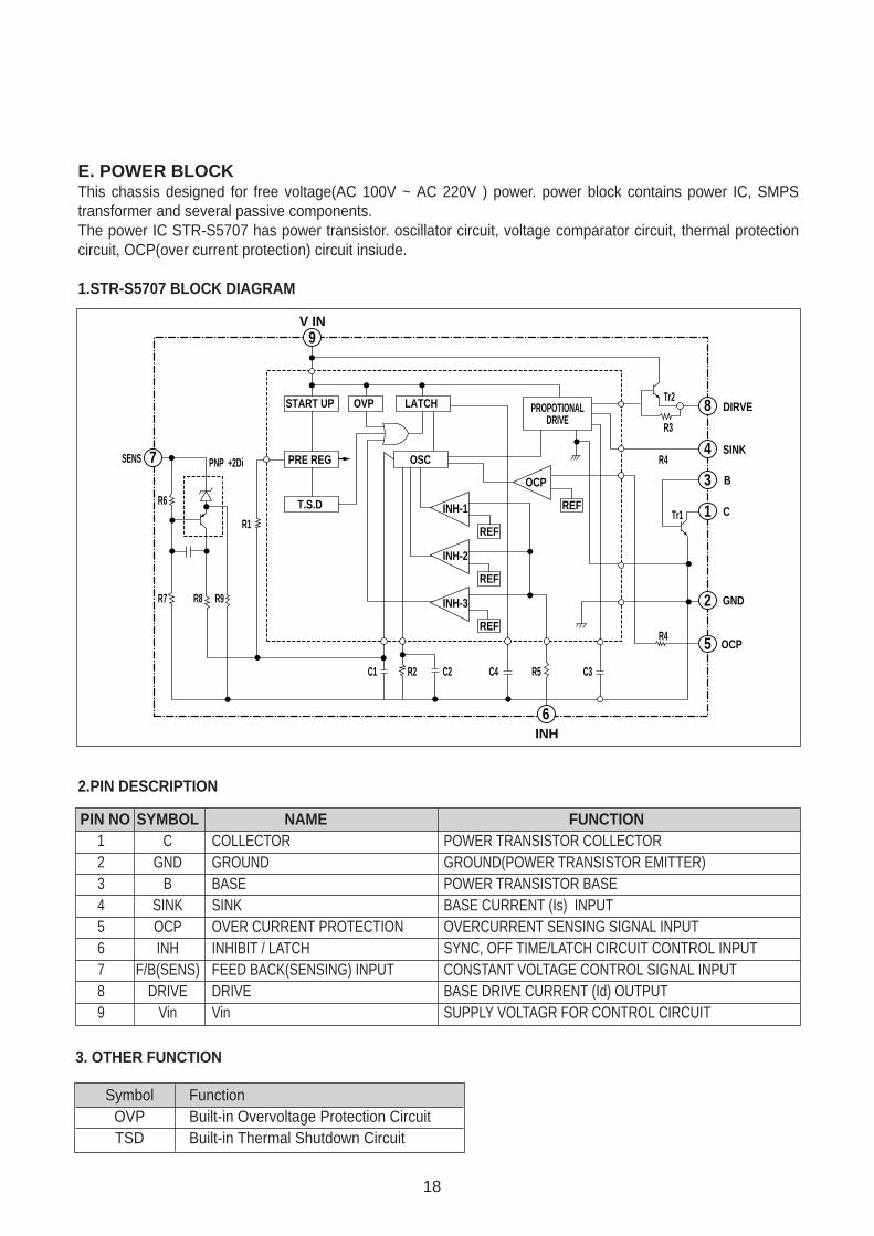
E. POWER BLOCKThis chassis designed for free voltage(AC 100V ~ AC 220V ) power. power block contains power IC, SMPStransformer and several passive components.The power IC STR-S5707 has power transistor. oscillator circuit, voltage comparator circuit, thermal protectioncircuit, OCP(over current protection) circuit insiude.
1.STR-S5707 BLOCK DIAGRAM
2.PIN DESCRIPTION
INH-1
REF
OCP
REF
INH-2
REF
INH-3
REF
9
7
6
8
4
3
1
2
5
START UP
PRE REG OSC
T.S.D
OVP LATCH
V IN
INH
PROPOTIONALDRIVE
Tr2
R6
PNP +2Di
R7 R8 R9
Tr1
R4
R4
R3
R1
C1 C4 R5C2 C3R2
DIRVE
SINK
B
C
GND
OCP
SENS
PIN NO SYMBOL NAME FUNCTION1 C COLLECTOR POWER TRANSISTOR COLLECTOR2 GND GROUND GROUND(POWER TRANSISTOR EMITTER)3 B BASE POWER TRANSISTOR BASE4 SINK SINK BASE CURRENT (Is) INPUT5 OCP OVER CURRENT PROTECTION OVERCURRENT SENSING SIGNAL INPUT6 INH INHIBIT / LATCH SYNC, OFF TIME/LATCH CIRCUIT CONTROL INPUT7 F/B(SENS) FEED BACK(SENSING) INPUT CONSTANT VOLTAGE CONTROL SIGNAL INPUT8 DRIVE DRIVE BASE DRIVE CURRENT (Id) OUTPUT9 Vin Vin SUPPLY VOLTAGR FOR CONTROL CIRCUIT
3. OTHER FUNCTION
Symbol FunctionOVP Built-in Overvoltage Protection CircuitTSD Built-in Thermal Shutdown Circuit

19
Rs(R803,R804) Ln
L1
9VIN
2GND
C806
D804
ACIN
Fig .1 Start-up Circuit
1
Fig .2 VIN Terminal Voltage Circuit Current VIN
IN20mA
200µA
4.9V 7.5V 8V Vin
4. EXPLAINATION OF CIRCUIT OPERATION1) VIN terminal, start-up circuitA start-up circuit is to start and stop a operation of a control IC by detecting a voltage appearing at a VIN
terminal (pin-9). At start up of a power supply, when a voltage at the VIN terminal reaches to 8V by charging upC806 by the function of a start-up resistor, Rs, a control circuit starts operating by the function of the start-upcircuit. As shown in Fig. 2, since a circuit current is suppressed 200§¸maximum ( at VIN = 7.5V ) until thecontrol circuit starts its operation.
After the control circuit starts its operation, power source is obtained by smoothing voltage appearing at L1winding. Once the control circuit starts operating, as its voltage doesn’t reach the fixed voltage at once, VIN
terminal voltage starts dropping. However, as a shut-down voltage is set low (at 4.9V), while VIN terminalvoltage reaches a shutdown voltage, L1 winding voltage reaches the fixed voltage earlier so that the controlcircuit can continue on operating.
2) Osciliator, F/B terminal voltage (Pin #7)A oscillator generates pulse signals which turns a power transistor on and off by making use of charge anddischarge of CI and C2 incorporated in the Hybrid IC.Constant voltage control of a switch-mode power supply is performed by changing both ON- time and OFF-time except when the load is light (ex. remote control stand-by mode of TVs).Fig. 4 shows how the oscillator works when the Hybrid IC independently operates (with no F/B nor INHsignals). When the power thransistor is on, C2 Is charged to the set voltage (approx 2.3V at Ta =25°C). On theother hand, C1 starts charging up through R1 from almost 0V and the voltage across C1 increases inaccordance with the inclination determined by the product of C1 and R1. When the voltage across C1 reachesapprox. 0.75V (Tc=25°C). the output from the oscillator is reversed and the power transistor turns off. At thesame time C1 is quickly discharged by the function of a internal circuit of the oscillator and the voltage across itdecreases to almost 0V. When the power transistor turns off, C2 starts discharging through R2 and the voltageacross C2 decreases in accordance with the inclination derermined by the product of C2 decreases to about1V. the output from the oscillator is reversed again and the transistor consequently turns on. The powertransistor continues turning on and off by repeating the above-mentioned operations.

20
As the circuit in Fig. 3 shows, the ON-time is controlled by changing a current charged by C1, which is as theresult of that the detection winding (L1),which detects a change of voltage in a secondary side, connected to thesensing terminal (Pin No. 7) has the current in accordance with an output signal from an output voltagedetection circuit (an error amplifier) built in. As an AC input voltage to the power supply gets the higher and aload current the smaller, the current flowing to the SENS terminal gets the larger, and the ON-time gets theshorter.
3) Function of INH terminal (Pin #6), control of OFF-timeSignal to the INH terminal is used as inputs to COMP.1 and COMP.2 inside of the control IC. A threshold voltageof COMP.1 VTH1 is set at 0.75V (Ta=25°C) and an input signal to a drive circuit becomes almost 0V (the powertransistor is in OFF mode) when a voltage at the INH terminal reaches the VTH1. As long as the INH terminalvoltage does not get lower than VTH1. the power transistor sustains OFF mode. On the other hand, a thresholdvoltage of COMP.2 VTH2, is set at 1.5V (Ta=25°C).When the INH terminnal voltage reaches VTH2, an output fromCOMP.2 reverses and, as a result, C2 starts firing and a voltage across C2 drops to almost 0V in a moment. Asthe result of this immediate discharge of C2, the OFF-time of the oscillator which has been determined by theproduct of C2 and R2 (⁄ 55 ¥ sec) can be quicker up to approx. 2¥sec. As long as the INH terminal voltagedoes not get lower than VTH2, AVoltage across C2 stays at almost 0V and a output from the oscillator keeps thepower transistor being on. The relation between the INH terminal voltage and the function of the oscillatordescribed above is shown in Fig. 6 and Fig. 7
R6
R7 PIN +2Di
Reg
DriveCfrcu1
R7 R8 R9
R1
R2C1 C2
+–+–
OSD
L1
COMP 1
COMP 2
VTH1
VTH2
INHTre
Fig 3 Oscillator Circuit Configulation
C2 ACROSSVoltage
C1 ACROSSVoltage
Osc.Output
PTR
Fig 4 Operation Waveforms of Oscillator without F/B nor INH Signal
1V
2.3V
0V
0V ONOFF
0.75V
Fig 5 Operation Waveforms of Oscillator with F/B Signal
C2 ACROSSVoltage
C1 ACROSSVoltage
Osc.Output
PTR
1V
2.3V
0V
0V
0.75V
OFF
Ter. Voltage
Osc.Output
PTR
Fig .6 Operation Waveforms of INH Terminal(VTH1)
ON
INH VTH1
C2 ACROSSVoltage
Osc.Output
PTR
Fig .7 Operation Waveforms of INH Terminal(VTH2)
2.3V
ON OFF
Ter. Voltage.INH
VTH2
0V

21
9VIN 6
INH
2GND
C808
R807 L1
D805
D803
S1+
Fig 8 Operation Circuit
Fig. 9 shows waveforms of VCE, Ic and VINH of the transistor, voltage across C808 in the oscillator as well as anoutput from the oscillator when operating in quasi-resonant mode.
when the power transistor turns off and a voltage higher than VTH2 is applied to the INH terminal, C808immediately discharges and then starts charging again. Even after the discharge of energy of a secendarywinding is completed, VINH does not immediately increases. When it gets lower than VTH2 after the time,tr, whichis determined by the production of internal impedance of the IC and CINH, has past, the transistor turns on.
4) Quasi-resonant operationBy inputting a voltage signal which is synchronized with the energy discharge time of a secondary winding of atransformer to the. INH terminal, quasi-resonant operation can be achieved. As shown in Fig. 8 , the voltage ofL1 winding which is synchronized. with the energy discharge time of a secondary winding. S1. shall be input tothe INH terminal through D805 and R807. Since VTH2 is set at 1.5V typical, a voltage at the INH terminal. VINH,shall be set at 2V.
0V
0V
Fig 9 Waveforms of VCE and VINH at Quasi-resonant Operation
VCE
INH Terminal
Voltage
tr
VTHI

22
5) Drive circuitThe STR-S5707 applies the proportional drive system in order to minimize turn-on and satruration loss, andstorage time. In the conventional RCC system, turn-on loss and switching noise due to the surge currentappearing when the power transistor turns on are high as because the transistor is driven by the drive currentshown in Fig. 10-1. In addition, since is decreases linearly when the transistor turn off and a peak value of IB2 isnot large, the storage time is long and the VCE(sat) voltage is high, which results in large turn-off loss. The circuitand the waveforms of the proportional drive system which is applied to the STR-S5707 in order to reduce theseswitching loss and shorten the storage time are shown in Fig . 10 and Fig. 10-2 respectively.
OSCDrive
R810
C805
D806
Fig .10 D806 and C805 function to reverse-blas between the base and the emitter of the transistor during its off state.
Fig .10-1 Waveforms of Conventional RCC Power Supply
Fig .10-2 Waveforms of power Supply Using STR-S5707
VCE
IC
0
VCE
IC
0
VBE
IB
Reveresbias
VBE
IB
Reveresbias

23
6) OCP (overcurrent protection) functionOvercurrent protection is performed pulse by pulse by directly detecting collector current of the power transistor.Configuration of the OCP circuit is shown in . Detecting voltage is set to -1V below a reference point of GND(ground). In additlon, since the detecting voltage is set by a comparator, very stable characteristics againsttemperature is achieved and drift of the detecting voltage against temperature change is almost 0V.
7) Latch circuitIt is a circuit which sustains an output from the oscillator low and stops operation of the power supply whenovervoltage protection (OVP) circuit and thermal shutdown (TSD) circuit are in operation. As the sustainingcurrent of the latch circult is 500¥A maximum when VIN terminal voltage is 4V. the power supply circuit sustainsthe off state as long as current of 500¥A minimum flows to VIN terminal from a start-up resistor. In order toprevent a malfunction to be caused by a noise and so on, delay time is provided by C1 incorporated in the ICand, therefore, the latch circuit operates when the OVP of TSD circuit is in operation, of an external signal inputis provided. for about 10¥sec or longer.In addition, even after the latch circuit start operating, the constantvoltage regulator (Reg) circuit is in operation and the circuit current is at high level. As a result. VIN terminalvoltage rapidly decreases. When VIN terminal voltage becomes lower than the shutdown voltage, VIN(OFF),(4.9V typical), it starts in -creasing as the circuit current is below 500¥A. When it reaches the ON-state voltage.VIN(ON), (8V typical), VIN terminal voltage starts decreasing because the circult current increases again.
Drive
OSC +–
-1V
5.OCP2.GND
R811
Fig 11 Overcurrent protection Circuit

24
when the latch cirguit is on. VIN terminal voltage increases and decreases with- in the range from 4.9V typical to8V typical and is prevented from abnormally rising. Fig. 12 shows an example of VIN terminal voltagewaveform.Cancellation of the latch-is done by decreasing VIN terminal voltage below 3.3V. The power supplycan be restarted after disconnecting an AC input to the power supply once.
8) Thermal shutdown, circuitIt is a circuit to trigger the latch circuit when the frame temperature of the IC exceeds 150°C (typical). Althoughthe temperature is actually sensed at the control chip. It works against overheating of the power transistor asthe power transistor and the control IC are mounted on the same lead frame.
9) Overvoltage protection circuit
It is a circuit to trigger the latch circuit when VIN terminal voltage exceeds 11V (typical). Although it basicallyfunctions as protection of VIN terminal against overvoltage, since VIN terminal is usually supplied from the drivewinding of the transformer and the voltage is proportional to the output voltage, it also functions against theovervoltage of secondary output which causes when the control circuit opens or in some other events.
Fig 12 Typical VIN Terminal Voltage Waveform When Latch Circuit Is Operating
8V(TYP)
VIN
4.9V(TYP)
0

25
5.OCP (OVER CURRENT PROTECTION) CIRCUITThis circuit is designed to protect the circuit from over current due to overload occurred at the rear of 132[V]line.
1) CONFIGURATION OF OCP CIRCUIT
2) EXPLANATION OF THE OPERATION
¤ There is very little voltage drop at £ R821(1W 0.68) of 123 [V] line.¤ŁIn case that the overload occurs at the rear of 123[V] line, the increase of the voltage drop at R821 bring
down the base voltage of the Q806 so as to drive the Q806¤ØBecause of the overload at the rear of the R821, the voltage of the £ point decreases. And this makes Q806
turn on so that a voltage is applied to the #29 of I701.¤ŒIn case that OCP operates by the #29 of the I701, the set is protected by power off (#32 of I701¡ LOW).
+
C816100µ16V
R821
123 [V] LINE1W 0.68(F)
R82022K1/4W
R8238.2K1/4W
C8154.7µ50V
Q806KSA1013Y
R82220K1/4W
R82620K1/4W
D810UZ-5.1
R82422K1/4W
I701 #29(OCP)
FBTA
C
B

26
F.IC BLOCK DIAGRAM1.LA7688: VIF/SIF/VIDEO/CHROMA/DEFLECTION 1-CHIP IC
1
2
3
4
5
6
7
8
9
10
11
12
13
14
15
16
17
18
19
20
21
22
23
24
25
26
SIF IN
RF AGC VR
APC1 FILTER
AUDIO FILTER
VCO
VCO
AFT OUT
COMP. VIDEO OUT
INT VIDEO IN
CONTRAST
EXT. AUDIO IN
SHARPNESS
EXT. VIDEO IN
GND
VIDEO OUT
COLOR
TINT
BRIGHTNESS
VERT. OUT
50/60
AFC
HOR. X-TAL
HOR. VCC
HOR. OUTPUT
FBP IN/BGP OUT
52
51
50
49
48
47
46
45
44
43
42
41
40
39
38
37
36
35
34
33
32
31
30
29
28
27
FM-DET OUT
AUDIO OUT
RF AGC OUT
IF GND
VIF INPUT
VIF INPUT
IF AGC
VIF VCC
SIF VCC
APC FILTER
X-TAL
X-TAL
VCC
DEMO OUTUT(R-Y)
DEMO OUTUT(R-Y)
ALC INPUT(R-Y)
ALC INPUT(B-Y)
R-OUT
G-OUT
B-OUT
BLACK STRETCH
OSD R
OSD G
OSD B
OSD Ys IN
X-TAL SW
FILTER-REF/S-VHS SW

27
2.µ-COM : DMC42C200N
1
2
3
4
5
6
7
8
9
10
11
12
13
14
15
16
17
18
19
20
40
39
38
37
36
35
34
33
32
31
30
29
28
27
26
25
24
23
22
21
NTSC-M
PAL-M
AC DOWN DETECT
SD
REMOCON IN
KEY IN 0
KEY IN 1
KEY IN 2
KO 0
(TIMER)
KO 1
KO 2(CLOCK)
(DATA)
ENABLE
AFC
TINT
COLOR
SHARP
CONTRAST
BRIGHT
VOLUME
/S.MUTE(OPEN DRAIN)
/V.MUTE(OPEN DRAIN)
TV/VIDEO(OPEN DRAIN)
POWER
SCREEN OUT(PUSE-PULL)
OCP IN
50/60 IN
C. IDENT IN(PUSH PULL)
osd IN
OSD B
OSD G
OSD R
RCO/PWM14
R83
RO3/INT3
RO2/INT2
RO1/INTO/TIMI
ROO/INTO/TIMO
XIN
XOUT
/RESET
R82
GND
R81
R80
Vcc
R23
R22
R20/PCL
R21/AFC IN
OSC IN
OSC out
RC1/PWM60
RC2/PWM61
RC3/PWM62
PWM80
PWM81
PWM82
R30
R31
R32
R33
R10
R11
R12
R13
OSD Ys
OSD B
R61/OSD G
R60/OSD R
/VS
/HS

28
3.LC89950 : CCD DELAY LINE
B-YIN 5
B-YOUT3
RD2
OUT1
VSS14
BGPIN13
VDD12
VDD 6
R-YIN 7
4MHzOUT 8
COMP 9
PC OUT
11
VCO IN
10
VSS4
Ø1 Ø2
Ø1 Ø2
CLAMP
CLAMP
AUTO BIAS
AUTO BIAS
BGP
BGP
4MHz OSC.
DUTY Compensation
vco
CCD254.5 BIT
CCD254.5 BIT
CLOCK DRIVER
TIMING
1/256 COUNTER
(S&H.AMP)
(S&H.AMP)
Pump-up
BGP
BGP
Wave Forming
Phase comporator

29
3.LOCAL KEY & OPTION SW
6
10
12
13
15
16
KEY IN 0
KEY IN 1
KEY IN 2
KEY -O 0
KEY -O 1
KEY -O 2
ROO/INTO/TIMO
R82
I701
R81
R80
R23
R22
CH –
CH +
AUTO-ON TV/VID LANGUAGE
VOL – MENU
VOL +
30
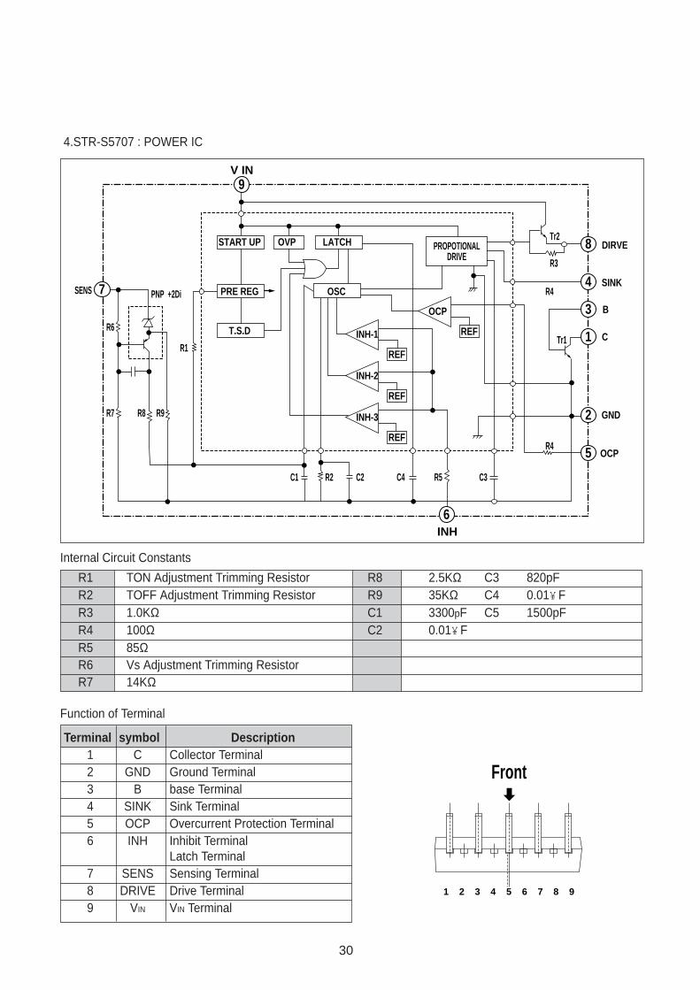
4.STR-S5707 : POWER IC
INH-1
REF
OCP
REF
INH-2
REF
INH-3
REF
9
7
6
8
4
3
1
2
5
START UP
PRE REG OSC
T.S.D
OVP LATCH
V IN
INH
PROPOTIONALDRIVE
Tr2
R6
PNP +2Di
R7 R8 R9
Tr1
R4
R4
R3
R1
C1 C4 R5C2 C3R2
DIRVE
SINK
B
C
GND
OCP
SENS
Internal Circuit Constants
Function of Terminal
R1 TON Adjustment Trimming Resistor R8 2.5KΩ C3 820pFR2 TOFF Adjustment Trimming Resistor R9 35KΩ C4 0.01¥FR3 1.0KΩ C1 3300pF C5 1500pFR4 100Ω C2 0.01¥FR5 85ΩR6 Vs Adjustment Trimming ResistorR7 14KΩ
Terminal symbol Description1 C Collector Terminal2 GND Ground Terminal3 B base Terminal4 SINK Sink Terminal5 OCP Overcurrent Protection Terminal6 INH Inhibit Terminal
Latch Terminal7 SENS Sensing Terminal8 DRIVE Drive Terminal9 VIN VIN Terminal
1 2 3 4 5 6 7 8 9
Front

31
5.LA7837 : VERTICAL IC
Power supply (+B1)
Vertical trigger input
Time constant
Vertcal height control
50/60Hz vertical sizecontrol signal input
Ramp wavefom generation
AC/DC feedback input tovertcal output section
Power supply (+B8)
Pump-up output
OSC blocking
GND
vertcal output
Power supply for vertical output
12
34
56
78
910
1112
13
VertTingInput
OneShotMulti
PumpUp
Vert.Drive
Ramp
Generator
Vert.SizeControlS.W
.
Vert.out
Thermal protection

32
§ TROUBLE SHOOTING CHARTS¡ÆNO SOUND
OK
OK
OK
OK
OK
OKOK
NG
NG
NG
NG
NG
CHECK THE SPEAKER
CHECK THE VOLTAGE OFPIN 2 OF I601
CHECK THE PIN 6 AND 8OF I601 AT THAT
SOUND VOLUME MAX.
CHECK THE PIN 51 OF I501
CHECK AFT AND CHECK THEPIN 52 VOLTAGE OF I501
CHECK/REPLACE Z501
REPLACE SPEAKER
CHECK/REPLACER606, I601
CHECK PIN 5 OF I601
CHECK/REPLACE I701
CHECK/REPLACE C604
REPLACE I501
OK
OK
OK
OK
NG
NG
NG
TURN OFF THE MAIN POWER SW AND TURN ON THE TV SET AGAIN
CHECK THE WAVEFORM OF PIN 23, 24, 25, 26 OF I701
CHECK THE WAVE FROM OFPIN 21, 22 OF I701
REPLACE I701CHECK THE WAVEFORM OFQ704
CHECK/REPLACE R771, 772, 773514, 587, C514, 515, AND 516
CHECK/REPLACE I501 CHECK/REPLACE I501, R759 CHECK/REPLACEQ704
¡ÆNO NO-SCREEN DISPLAY
33
OK
OK
OK
OK
OK
OK
NG
NG
NG
NG
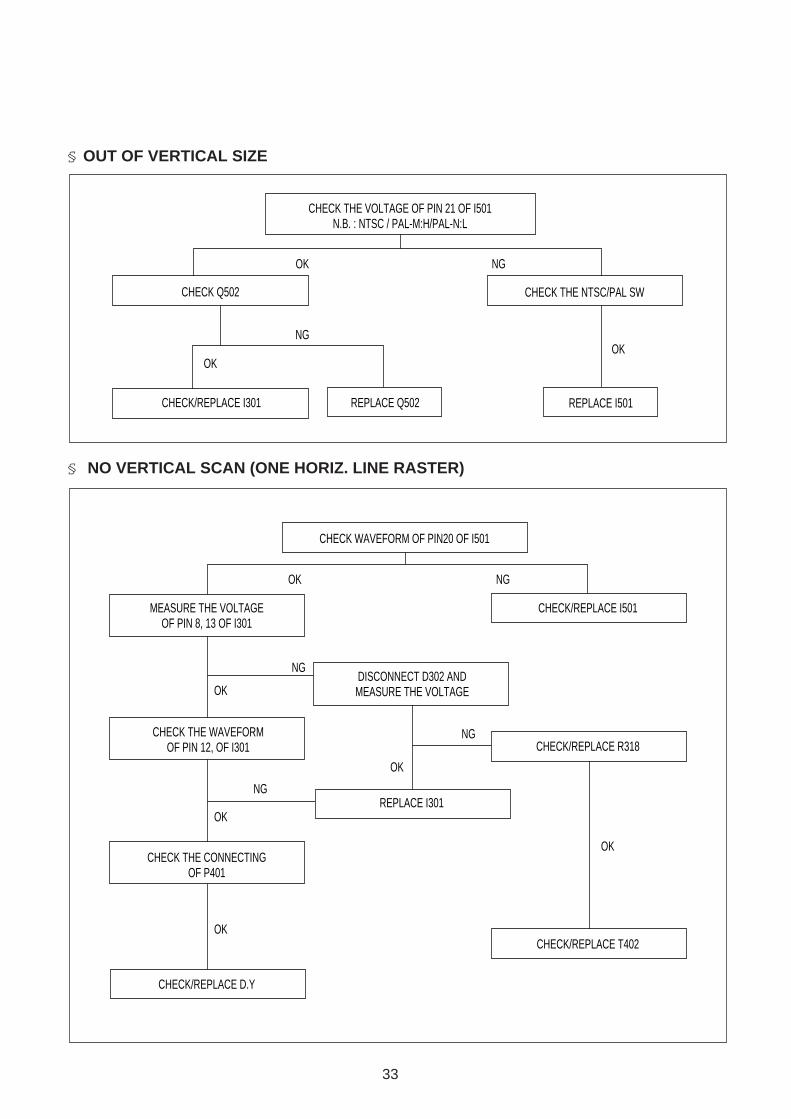
CHECK WAVEFORM OF PIN20 OF I501
MEASURE THE VOLTAGEOF PIN 8, 13 OF I301
CHECK THE WAVEFORMOF PIN 12, OF I301
CHECK THE CONNECTINGOF P401
CHECK/REPLACE D.Y
DISCONNECT D302 ANDMEASURE THE VOLTAGE
REPLACE I301
CHECK/REPLACE R318
CHECK/REPLACE T402
CHECK/REPLACE I501
OK
OKOK
NG
NG
CHECK THE VOLTAGE OF PIN 21 OF I501N.B. : NTSC / PAL-M:H/PAL-N:L
CHECK Q502
CHECK/REPLACE I301 REPLACE Q502
CHECK THE NTSC/PAL SW
REPLACE I501
§ OUT OF VERTICAL SIZE
§ NO VERTICAL SCAN (ONE HORIZ. LINE RASTER)

34
OK
OK
OK
OK
NGNG
CHECK THE VOLTAGE OF PIN21 OF I501 (HIGH)
CHECK/REPLACE Q502 CHECK PIN 17 OF I501
REPLACE X501, C507
CHECK/REPLACE I701CHECK/REPLACE I501
REPEAT ON COLOR (GENERAL) PROCESS
CHECK/REPLACEI501
OK NG
NG
NG
RECEIVE A COLOR BAR SIGNALWITH PATTERN GENERATOR
CHECK THE CONTROL VOLTAGE OF I701 #39(PUSH THE REMOCON CONTROL BUTTON FOR COLOR MAX)
CHECK THE COLOR/KILLERVOLTAGE OF I501 #17
CHECK THE COMPOSIT VIDEOSIGNAL ON #10 OF I501
CHECK/REPLACE I501
CHECK/REPLACE I701
CHECK/REPLACE R527, L502, Z502,Q503, R525 AND R528
§ NO COLOR (GENERAL)
§ NO COLOR (AT PAL-N ONLY)

35
OK
OK
OK
OK
NG
NG
NG
RECEIVE A COLOR BAR SIGNALWITH SIGNAL GENERATOR
WHETHER IS THE COLORNORMAL OR NOT?
CHECK I701 AND ANTENNA
CHECK/REPLACE
REPLACE I701
REPLACE D508
CHECK THE VOLTAGE OF PIN1AND PIN 27 OF I701 (HIGH)
CHECK D508
CHECK/REPLACE X502 AND C508
CHECK/REPLACE I501
OK
OK OK
OK
OK
NG
NG
NGNG
NG
CHECK THE VOLTAGE OF PIN21 OF I501 (HIGH)
CHECK PIN 27 OF I701(HIGH)
CHECK THE PIN 2 OFI701 (HIGH)
CHECK THE PIN 18 OFI501 (LOW)
CHECK THE CCD DELAYLINE (I502)
CHECK/REPLACEQ502 AND I701
CHECK/REPLACE Q702
CHECK PIN 22 AND 23OF I501
CHECK/REPLACEC517, C518, R532
AND X401
CHECK/REPLACEI501
§ ON COLOR (AT PAL-M ONLY)
§ ON COLOR (AT NTSC ONLY)

36
OK
OK OK
OK
NG
NG NG
NG
OPEN THE SLIT OF TUNER IF OUTPUT ANDCONNECT TESTER LEADS TO PIF INPUT STAGE
(C101) AND EARTH MOMENTARILY
NOISE IS APPEARED OR NOT?
MEASURE THE VOLTAGE OFEACH PIN OF I501
CHECK/REPLACE Z101(SAW FILTER)
CHECK/REPLACEI501
CHECK/REPLACE I501AND PIF AGC
CIRCUIT
MEASURE THEB+ VOLTAGE OF
TUNER
CHECK/REPLACE+9V LINE
CHECK/REPLACETUNER
MEASURE THE VOLTAGE OFAGC TERMINAL OF TUNER
(NORMAL: +3.0V~+7.6V)
OK
OK
LOW OR ZERO
OK
CHECK +9V/+7.6V LINE ON MAIN PCB
CHECK/REPLACE R202, I201
CHECK/REPLACE D201, R201
CHECK/REPLACEI501
CHECK/REPLACE U101
§ NO RASTER (NOISE OR WEAK SOUND)
§ NO PICTURE (RASTER REMAINS AND NO SOUND)

37
OK
OK
OK
OK
OK
OK
NG
NG NG
HEATER ELEMENTS OF CRTARE LIGHTING OR NOT?
CHECK H.V ATANODE OF CRT
CHECK CONNECTORASS' Y P401 AND PA501
CHECK/REPLACE I501
CHECK/REPLACET402
CHECK THE SUPPLYVOLTAGE OF HEATER
CHECK/REPLACETHE WIRING
PA501 AND P401
CHECK/REPLACER817 AND T402
CHECK/REPLACE HORIZ.DRIVE TRANS(T401)
CHECK/REPLACE Q401/Q402
OK
OK
OK
OK
OK
OK
OK
NG
NG
NG
CHECK WHETHER THE BRIGHT & CONTRAST ARECONTROLLABLE OR NOT?
CHECK/REPLACE THE COMPOSITESIGNAL INPUT STAGE
AND VIDEO PARTS OF I501
CHECK THE VCC VOLTAGE AT#40 OF I501
CHECK R, G, B SIGNALOUTPUT AND PA501
CHECK/REPLACE +7.6VLINE OF I501
CHECK THE VOLTAGE OF+185V ON CRT BOARD
CHECK/REPLACE +185VCHECK/REPLACE THEEACH PIN OF I501
CHECK THE SIGNAL INPUTCIRCUIT OF I501
REPLACE THE SIGNALINPUT CIRCUIT
REPLACE T402
§ NO PICTURE (RASTER AND SOUND OK)
§ NO RASTER (SOUND OK)

38
OK
OK
OK
OK
OK
NG
NG
NG
NG
CHECK THE PIN 14 OF I501
CHECK THE AV SIGNAL OFAV JACK JV01 AND JV02
CHECK/REPLACEC540, CA01, RV02,RA01
CHECK/REPLACEI501
CHECK/REPLACE AVJACK JV01 AND JV02
CHECK #33OF I701
CHECK/REPLACEI501
CHECK THE DC VOLTAGE AT#1 OF I501
CHECK/REPLACEI701
CHECK/REPLACE R555,R556, R562 AND Z501
§ AV DOES NOT OPERATE (TV SIGNAL IS OK)

39
OK
NG
OK
OK
OK
OK
OK
OK
NG
NG(140V OR MORE)
NG
NG
NG(OV)
NG
CHECK FUSE F801ON MAIN PCB
REPLACE THE FUSE
NEW FUSE ALSO OPENS
CHECK AND REPLACED802, I801
CHECK +123V LINEON MAIN PCB
CHECK 5.1V LINE OFMAIN PCB
CHECK/REPLACED809 AND D704
CHECK/REPLACE +11V,+9V AND +180V
CHECK/REPLACE Q801,Q802 AND I802
CHECK/REPLACE I701
CHECK/REPLACE I501
CHECK/REPLACE HORIZ.OUTPUT DRIVE CIRCUIT
CHECK/REPLACET801 AND I801
CHECK THE VOLTAGEAT PIN 9 OF I801
CHECK/REPLACED827 AND Q827
CHECK/REPLACE I801
§ POWER FAILS TO TURN ON (NO RASTER, NO SOUND DOES NOT TURN ON)
41
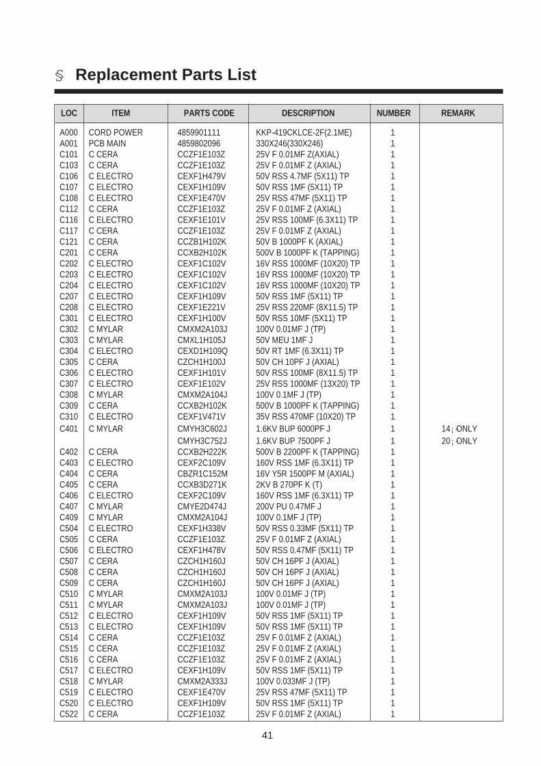
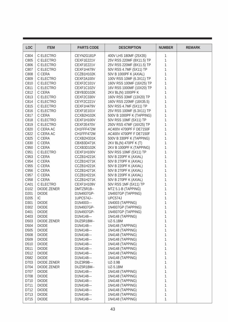
LOC ITEM PARTS CODE DESCRIPTION NUMBER REMARK
A000 CORD POWER 4859901111 KKP-419CKLCE-2F(2.1ME) 1A001 PCB MAIN 4859802096 330X246(330X246) 1C101 C CERA CCZF1E103Z 25V F 0.01MF Z(AXIAL) 1C103 C CERA CCZF1E103Z 25V F 0.01MF Z (AXIAL) 1C106 C ELECTRO CEXF1H479V 50V RSS 4.7MF (5X11) TP 1C107 C ELECTRO CEXF1H109V 50V RSS 1MF (5X11) TP 1C108 C ELECTRO CEXF1E470V 25V RSS 47MF (5X11) TP 1C112 C CERA CCZF1E103Z 25V F 0.01MF Z (AXIAL) 1C116 C ELECTRO CEXF1E101V 25V RSS 100MF (6.3X11) TP 1C117 C CERA CCZF1E103Z 25V F 0.01MF Z (AXIAL) 1C121 C CERA CCZB1H102K 50V B 1000PF K (AXIAL) 1C201 C CERA CCXB2H102K 500V B 1000PF K (TAPPING) 1C202 C ELECTRO CEXF1C102V 16V RSS 1000MF (10X20) TP 1C203 C ELECTRO CEXF1C102V 16V RSS 1000MF (10X20) TP 1C204 C ELECTRO CEXF1C102V 16V RSS 1000MF (10X20) TP 1C207 C ELECTRO CEXF1H109V 50V RSS 1MF (5X11) TP 1C208 C ELECTRO CEXF1E221V 25V RSS 220MF (8X11.5) TP 1C301 C ELECTRO CEXF1H100V 50V RSS 10MF (5X11) TP 1C302 C MYLAR CMXM2A103J 100V 0.01MF J (TP) 1C303 C MYLAR CMXL1H105J 50V MEU 1MF J 1C304 C ELECTRO CEXD1H109Q 50V RT 1MF (6.3X11) TP 1C305 C CERA CZCH1H100J 50V CH 10PF J (AXIAL) 1C306 C ELECTRO CEXF1H101V 50V RSS 100MF (8X11.5) TP 1C307 C ELECTRO CEXF1E102V 25V RSS 1000MF (13X20) TP 1C308 C MYLAR CMXM2A104J 100V 0.1MF J (TP) 1C309 C CERA CCXB2H102K 500V B 1000PF K (TAPPING) 1C310 C ELECTRO CEXF1V471V 35V RSS 470MF (10X20) TP 1C401 C MYLAR CMYH3C602J 1.6KV BUP 6000PF J 1 14¡–ONLY
CMYH3C752J 1.6KV BUP 7500PF J 1 20¡–ONLYC402 C CERA CCXB2H222K 500V B 2200PF K (TAPPING) 1C403 C ELECTRO CEXF2C109V 160V RSS 1MF (6.3X11) TP 1C404 C CERA CBZR1C152M 16V Y5R 1500PF M (AXIAL) 1C405 C CERA CCXB3D271K 2KV B 270PF K (T) 1C406 C ELECTRO CEXF2C109V 160V RSS 1MF (6.3X11) TP 1C407 C MYLAR CMYE2D474J 200V PU 0.47MF J 1C409 C MYLAR CMXM2A104J 100V 0.1MF J (TP) 1C504 C ELECTRO CEXF1H338V 50V RSS 0.33MF (5X11) TP 1C505 C CERA CCZF1E103Z 25V F 0.01MF Z (AXIAL) 1C506 C ELECTRO CEXF1H478V 50V RSS 0.47MF (5X11) TP 1C507 C CERA CZCH1H160J 50V CH 16PF J (AXIAL) 1C508 C CERA CZCH1H160J 50V CH 16PF J (AXIAL) 1C509 C CERA CZCH1H160J 50V CH 16PF J (AXIAL) 1C510 C MYLAR CMXM2A103J 100V 0.01MF J (TP) 1C511 C MYLAR CMXM2A103J 100V 0.01MF J (TP) 1C512 C ELECTRO CEXF1H109V 50V RSS 1MF (5X11) TP 1C513 C ELECTRO CEXF1H109V 50V RSS 1MF (5X11) TP 1C514 C CERA CCZF1E103Z 25V F 0.01MF Z (AXIAL) 1C515 C CERA CCZF1E103Z 25V F 0.01MF Z (AXIAL) 1C516 C CERA CCZF1E103Z 25V F 0.01MF Z (AXIAL) 1C517 C ELECTRO CEXF1H109V 50V RSS 1MF (5X11) TP 1C518 C MYLAR CMXM2A333J 100V 0.033MF J (TP) 1C519 C ELECTRO CEXF1E470V 25V RSS 47MF (5X11) TP 1C520 C ELECTRO CEXF1H109V 50V RSS 1MF (5X11) TP 1C522 C CERA CCZF1E103Z 25V F 0.01MF Z (AXIAL) 1
§ Replacement Parts List

42
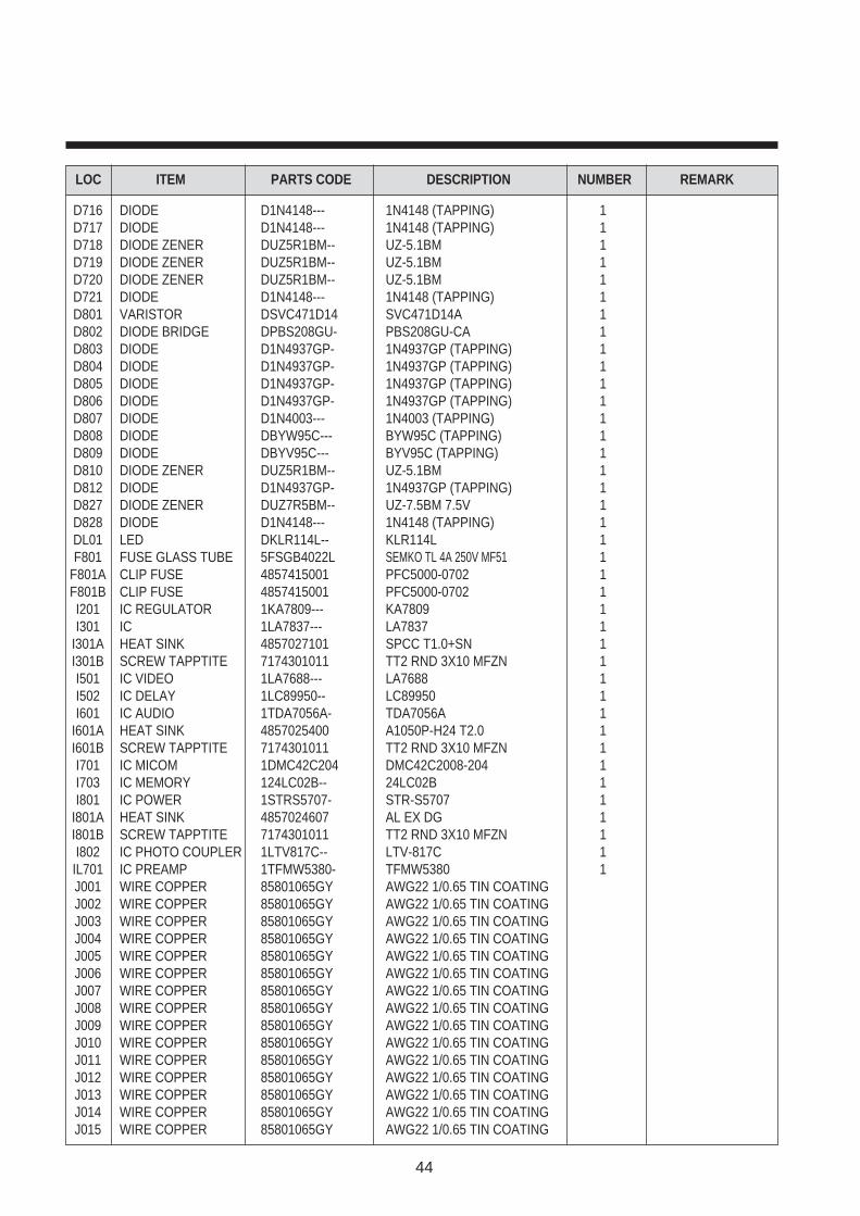
LOC ITEM PARTS CODE DESCRIPTION NUMBER REMARK
C523 C ELECTRO CEXF1H339V 50V RSS 3.3MF (5X11) TP 1C524 C ELECTRO CEXF1H478V 50V RSS 0.47MF (5X11) TP 1C525 C ELECTRO CEXF1H109V 50V RSS 1MF (5X11) TP 1C526 C CERA CCZB1H561K 50V B 560PF K (AXIAL) 1C527 C CERA CCZB1H102K 50V B 1000PF K (AXIAL) 1C528 C CERA CZSL1H510J 50V SL 51PF J (AXIAL) 1C529 C CERA CZSL1H330J 50V SL 33PF J (AXIAL) 1C530 C CERA CCZB1H561K 50V B 560PF K (AXIAL) 1C533 C MYLAR CMXM2A104J 100V 0.1MF J (TP) 1C534 C ELECTRO CEXF1H109V 50V RSS 1MF (5X11) TP 1C536 C ELECTRO CEXF1E470V 25V RSS 47MF (5X11) TP 1C537 C ELECTRO CEXF1E470V 25V RSS 47MF (5X11) TP 1C538 C CERA SEMI CBZF1H104Z 50V F 0.1MF Z (AXIAL) 1C539 C CERA CCZB1H102K 50V B 1000PF K (AXIAL) 1C540 C ELECTRO CEXF1H339V 50V RSS 3.3MF (5X11) TP 1C542 C CERA CCZF1E103Z 25V F 0.01MF Z (AXIAL) 1C543 C CERA CCZF1E103Z 25V F 0.01MF Z (AXIAL) 1C544 C CERA CCZF1E103Z 25V F 0.01MF Z (AXIAL) 1C546 C CERA CCZB1H121K 50V B 120PF K (AXIAL) 1C547 C ELECTRO CEXF1H479V 50V RSS 4.7MF (5X11) TP 1C551 C CERA CCZF1E103Z 25V F 0.01MF Z (AXIAL) 1C552 C CERA CCZF1E103Z 25V F 0.01MF Z (AXIAL) 1C553 C CERA CCZF1E103Z 25V F 0.01MF Z (AXIAL) 1C580 C ELECTRO CEXF1H100V 50V RSS 10MF (5X11) TP 1C603 C MYLAR CMXM2A123J 100V 0.012MF J (TP) 1C604 C ELECTRO CEXF1H109V 50V RSS 1MF (5X11) TP 1C606 C ELECTRO CEXF1C102V 16V RSS 1000MF (10X20) TP 1C607 C MYLAR CMXM2A103J 100V 0.01MF J (TP) 1C608 C CERA CCZF1H473Z 50V F 0.047MF Z (AXIAL) 1C702 C ELECTRO CEXF1E101V 25V RSS 100MF (6.3X11) TP 1C703 C CERA SEMI CBZF1H104Z 50V F 0.1MF Z (AXIAL) 1C704 C ELECTRO CEXF1C102V 16V RSS 1000MF (10X20) TP 1C705 C CERA SEMI CBZF1H104Z 50V F 0.1MF Z (AXIAL) 1C706 C CERA CZCH1H160J 50V CH 16PF J (AXIAL) 1C707 C CERA CZCH1H160J 50V CH 16PF J (AXIAL) 1C708 C CERA CZSL1H300J 50V SL 30PF J (AXIAL) 1C709 C CERA CZCH1H160J 50V CH 16PF J (AXIAL) 1C710 C ELECTRO CEXF1H109V 50V RSS 1MF (5X11) TP 1C711 C ELECTRO CEXF1H100V 50V RSS 10MF (5X11) TP 1C712 C CERA SEMI CBZF1H104Z 50V F 0.1MF Z (AXIAL) 1C713 C ELECTRO CEXF1H479V 50V RSS 4.7MF (5X11) TP 1C714 C ELECTRO CEXF1H100V 50V RSS 10MF (5X11) TP 1C715 C ELECTRO CEXF1H100V 50V RSS 10MF (5X11) TP 1C716 C ELECTRO CEXF1H100V 50V RSS 10MF (5X11) TP 1C717 C CERA CCZB1H102K 50V B 1000PF K (AXIAL) 1C720 C ELECTRO CEXF1H100V 50V RSS 10MF (5X11) TP 1C722 C CERA CCZB1H471K 50V B 470PF K (AXIAL) 1C723 C CERA SEMI CBZF1H104Z 50V F 0.1MF Z (AXIAL) 1C725 C CERA CCZB1H471K 50V B 470PF K (AXIAL) 1C726 C CERA CCZB1H471K 50V B 470PF K (AXIAL) 1C727 C CERA SEMI CBZF1H104Z 50V F 0.1MF Z (AXIAL) 1C801 C LINE ACROSS CL1UC3104M WORLD AC250V 0.1UF M R.47 1C802 C CERA CCYB3A472K 1KV B 4700PF K 1C803 C CERA CCYB3A472K 1KV B 4700PF K 1
43
LOC ITEM PARTS CODE DESCRIPTION NUMBER REMARK
C804 C ELECTRO CEYN2G181P 400V LHS 180MF (25X35) 1C805 C ELECTRO CEXF1E221V 25V RSS 220MF (8X11.5) TP 1C806 C ELECTRO CEXF1E221V 25V RSS 220MF (8X11.5) TP 1C807 C ELECTRO CEXF1H479V 50V RSS 4.7MF (5X11) TP 1C808 C CERA CCZB1H102K 50V B 1000PF K (AXIAL) 1C809 C ELECTRO CEXF2A100V 100V RSS 10MF (6.3X11) TP 1C810 C ELECTRO CEXF2C101V 160V RSS 100MF (16X25) TP 1C811 C ELECTRO CEXF1C102V 16V RSS 1000MF (10X20) TP 1C812 C CERA CBYB3D102K 2KV BL(N) 1000PF K 1C813 C ELECTRO CEXF2C330V 160V RSS 33MF (13X20) TP 1C814 C ELECTRO CEYF2C221V 160V RSS 220MF (18X35.5) 1C815 C ELECTRO CEXF1H479V 50V RSS 4.7MF (5X11) TP 1C816 C ELECTRO CEXF1E101V 25V RSS 100MF (6.3X11) TP 1C817 C CERA CCXB2H102K 500V B 1000PF K (TAPPING) 1C818 C ELECTRO CEXF1H100V 50V RSS 10MF (5X11) TP 1C819 C ELECTRO CEXF2E470V 250V RSS 47MF (16X25) TP 1C820 C CERA AC CH1FFF472M AC400V 4700PF F DE7150F 1C822 C CERA AC CH1FFF472M AC400V 4700PF F DE7150F 1C825 C CERA CCXB2H331K 500V B 330PF K (TAPPING) 1C830 C CERA CBXB3D471K 2KV BL(N) 470PF K (T) 1C950 C CERA CCXB3D102K 2KV B 1000PF K (TAPPING) 1C951 C ELECTRO CEXF1H100V 50V RSS 10MF (5X11) TP 1C953 C CERA CCZB1H221K 50V B 220PF K (AXIAL) 1C954 C CERA CCZB1H271K 50V B 270PF K (AXIAL) 1C955 C CERA CCZB1H221K 50V B 220PF K (AXIAL) 1C956 C CERA CCZB1H271K 50V B 270PF K (AXIAL) 1C957 C CERA CCZB1H221K 50V B 220PF K (AXIAL) 1C958 C CERA CCZB1H271K 50V B 270PF K (AXIAL) 1CA01 C ELECTRO CEXF1H109V 50V RSS 1MF (5X11) TP 1D102 DIODE ZENER DMTZ5R1B-- MTZ 5.1-B (TAPPING) 1D201 DIODE D1N4937GP- 1N4937GP (TAPPING) 1D205 IC 1UPC574J-- UPC574J 1D301 DIODE D1N4003--- 1N4003 (TAPPING) 1D302 DIODE D1N4937GP- 1N4937GP (TAPPING) 1D401 DIODE D1N4937GP- 1N4937GP (TAPPING) 1D403 DIODE D1N4148--- 1N4148 (TAPPING) 1D503 DIODE ZENER DUZ5R1BM-- UZ-5.1BM 1D504 DIODE D1N4148--- 1N4148 (TAPPING) 1D505 DIODE D1N4148--- 1N4148 (TAPPING) 1D508 DIODE D1N4148--- 1N4148 (TAPPING) 1D509 DIODE D1N4148--- 1N4148 (TAPPING) 1D510 DIODE D1N4148--- 1N4148 (TAPPING) 1D511 DIODE D1N4148--- 1N4148 (TAPPING) 1D512 DIODE D1N4148--- 1N4148 (TAPPING) 1D582 DIODE D1N4148--- 1N4148 (TAPPING) 1D703 DIODE ZENER DUZ3R9B--- UZ-3.9B 1D704 DIODE ZENER DUZ5R1BM-- UZ-5.1BM 1D707 DIODE D1N4148--- 1N4148 (TAPPING) 1D708 DIODE D1N4148--- 1N4148 (TAPPING) 1D710 DIODE D1N4148--- 1N4148 (TAPPING) 1D711 DIODE D1N4148--- 1N4148 (TAPPING) 1D712 DIODE D1N4148--- 1N4148 (TAPPING) 1D713 DIODE D1N4148--- 1N4148 (TAPPING) 1D715 DIODE D1N4148--- 1N4148 (TAPPING) 1
44
LOC ITEM PARTS CODE DESCRIPTION NUMBER REMARK
D716 DIODE D1N4148--- 1N4148 (TAPPING) 1D717 DIODE D1N4148--- 1N4148 (TAPPING) 1D718 DIODE ZENER DUZ5R1BM-- UZ-5.1BM 1D719 DIODE ZENER DUZ5R1BM-- UZ-5.1BM 1D720 DIODE ZENER DUZ5R1BM-- UZ-5.1BM 1D721 DIODE D1N4148--- 1N4148 (TAPPING) 1D801 VARISTOR DSVC471D14 SVC471D14A 1D802 DIODE BRIDGE DPBS208GU- PBS208GU-CA 1D803 DIODE D1N4937GP- 1N4937GP (TAPPING) 1D804 DIODE D1N4937GP- 1N4937GP (TAPPING) 1D805 DIODE D1N4937GP- 1N4937GP (TAPPING) 1D806 DIODE D1N4937GP- 1N4937GP (TAPPING) 1D807 DIODE D1N4003--- 1N4003 (TAPPING) 1D808 DIODE DBYW95C--- BYW95C (TAPPING) 1D809 DIODE DBYV95C--- BYV95C (TAPPING) 1D810 DIODE ZENER DUZ5R1BM-- UZ-5.1BM 1D812 DIODE D1N4937GP- 1N4937GP (TAPPING) 1D827 DIODE ZENER DUZ7R5BM-- UZ-7.5BM 7.5V 1D828 DIODE D1N4148--- 1N4148 (TAPPING) 1DL01 LED DKLR114L-- KLR114L 1F801 FUSE GLASS TUBE 5FSGB4022L SEMKO TL 4A 250V MF51 1
F801A CLIP FUSE 4857415001 PFC5000-0702 1F801B CLIP FUSE 4857415001 PFC5000-0702 1I201 IC REGULATOR 1KA7809--- KA7809 1I301 IC 1LA7837--- LA7837 1
I301A HEAT SINK 4857027101 SPCC T1.0+SN 1I301B SCREW TAPPTITE 7174301011 TT2 RND 3X10 MFZN 1I501 IC VIDEO 1LA7688--- LA7688 1I502 IC DELAY 1LC89950-- LC89950 1I601 IC AUDIO 1TDA7056A- TDA7056A 1
I601A HEAT SINK 4857025400 A1050P-H24 T2.0 1I601B SCREW TAPPTITE 7174301011 TT2 RND 3X10 MFZN 1I701 IC MICOM 1DMC42C204 DMC42C2008-204 1I703 IC MEMORY 124LC02B-- 24LC02B 1I801 IC POWER 1STRS5707- STR-S5707 1
I801A HEAT SINK 4857024607 AL EX DG 1I801B SCREW TAPPTITE 7174301011 TT2 RND 3X10 MFZN 1I802 IC PHOTO COUPLER 1LTV817C-- LTV-817C 1
IL701 IC PREAMP 1TFMW5380- TFMW5380 1J001 WIRE COPPER 85801065GY AWG22 1/0.65 TIN COATINGJ002 WIRE COPPER 85801065GY AWG22 1/0.65 TIN COATINGJ003 WIRE COPPER 85801065GY AWG22 1/0.65 TIN COATINGJ004 WIRE COPPER 85801065GY AWG22 1/0.65 TIN COATINGJ005 WIRE COPPER 85801065GY AWG22 1/0.65 TIN COATINGJ006 WIRE COPPER 85801065GY AWG22 1/0.65 TIN COATINGJ007 WIRE COPPER 85801065GY AWG22 1/0.65 TIN COATINGJ008 WIRE COPPER 85801065GY AWG22 1/0.65 TIN COATINGJ009 WIRE COPPER 85801065GY AWG22 1/0.65 TIN COATINGJ010 WIRE COPPER 85801065GY AWG22 1/0.65 TIN COATINGJ011 WIRE COPPER 85801065GY AWG22 1/0.65 TIN COATINGJ012 WIRE COPPER 85801065GY AWG22 1/0.65 TIN COATINGJ013 WIRE COPPER 85801065GY AWG22 1/0.65 TIN COATINGJ014 WIRE COPPER 85801065GY AWG22 1/0.65 TIN COATINGJ015 WIRE COPPER 85801065GY AWG22 1/0.65 TIN COATING
45
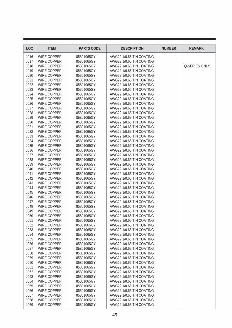
LOC ITEM PARTS CODE DESCRIPTION NUMBER REMARK
J016 WIRE COPPER 85801065GY AWG22 1/0.65 TIN COATINGJ017 WIRE COPPER 85801065GY AWG22 1/0.65 TIN COATINGJ018 WIRE COPPER 85801065GY AWG22 1/0.65 TIN COATING Q-SERIES ONLYJ019 WIRE COPPER 85801065GY AWG22 1/0.65 TIN COATINGJ020 WIRE COPPER 85801065GY AWG22 1/0.65 TIN COATINGJ021 WIRE COPPER 85801065GY AWG22 1/0.65 TIN COATINGJ022 WIRE COPPER 85801065GY AWG22 1/0.65 TIN COATINGJ023 WIRE COPPER 85801065GY AWG22 1/0.65 TIN COATINGJ024 WIRE COPPER 85801065GY AWG22 1/0.65 TIN COATINGJ025 WIRE COPPER 85801065GY AWG22 1/0.65 TIN COATINGJ026 WIRE COPPER 85801065GY AWG22 1/0.65 TIN COATINGJ027 WIRE COPPER 85801065GY AWG22 1/0.65 TIN COATINGJ028 WIRE COPPER 85801065GY AWG22 1/0.65 TIN COATINGJ029 WIRE COPPER 85801065GY AWG22 1/0.65 TIN COATINGJ030 WIRE COPPER 85801065GY AWG22 1/0.65 TIN COATINGJ031 WIRE COPPER 85801065GY AWG22 1/0.65 TIN COATINGJ032 WIRE COPPER 85801065GY AWG22 1/0.65 TIN COATINGJ033 WIRE COPPER 85801065GY AWG22 1/0.65 TIN COATINGJ034 WIRE COPPER 85801065GY AWG22 1/0.65 TIN COATINGJ035 WIRE COPPER 85801065GY AWG22 1/0.65 TIN COATINGJ036 WIRE COPPER 85801065GY AWG22 1/0.65 TIN COATINGJ037 WIRE COPPER 85801065GY AWG22 1/0.65 TIN COATINGJ038 WIRE COPPER 85801065GY AWG22 1/0.65 TIN COATINGJ039 WIRE COPPER 85801065GY AWG22 1/0.65 TIN COATINGJ040 WIRE COPPER 85801065GY AWG22 1/0.65 TIN COATINGJ041 WIRE COPPER 85801065GY AWG22 1/0.65 TIN COATINGJ042 WIRE COPPER 85801065GY AWG22 1/0.65 TIN COATINGJ043 WIRE COPPER 85801065GY AWG22 1/0.65 TIN COATINGJ044 WIRE COPPER 85801065GY AWG22 1/0.65 TIN COATINGJ045 WIRE COPPER 85801065GY AWG22 1/0.65 TIN COATINGJ046 WIRE COPPER 85801065GY AWG22 1/0.65 TIN COATINGJ047 WIRE COPPER 85801065GY AWG22 1/0.65 TIN COATINGJ048 WIRE COPPER 85801065GY AWG22 1/0.65 TIN COATINGJ049 WIRE COPPER 85801065GY AWG22 1/0.65 TIN COATINGJ050 WIRE COPPER 85801065GY AWG22 1/0.65 TIN COATINGJ051 WIRE COPPER 85801065GY AWG22 1/0.65 TIN COATINGJ052 WIRE COPPER 85801065GY AWG22 1/0.65 TIN COATINGJ053 WIRE COPPER 85801065GY AWG22 1/0.65 TIN COATINGJ054 WIRE COPPER 85801065GY AWG22 1/0.65 TIN COATINGJ055 WIRE COPPER 85801065GY AWG22 1/0.65 TIN COATINGJ056 WIRE COPPER 85801065GY AWG22 1/0.65 TIN COATINGJ057 WIRE COPPER 85801065GY AWG22 1/0.65 TIN COATINGJ058 WIRE COPPER 85801065GY AWG22 1/0.65 TIN COATINGJ059 WIRE COPPER 85801065GY AWG22 1/0.65 TIN COATINGJ060 WIRE COPPER 85801065GY AWG22 1/0.65 TIN COATINGJ061 WIRE COPPER 85801065GY AWG22 1/0.65 TIN COATINGJ062 WIRE COPPER 85801065GY AWG22 1/0.65 TIN COATINGJ063 WIRE COPPER 85801065GY AWG22 1/0.65 TIN COATINGJ064 WIRE COPPER 85801065GY AWG22 1/0.65 TIN COATINGJ065 WIRE COPPER 85801065GY AWG22 1/0.65 TIN COATINGJ066 WIRE COPPER 85801065GY AWG22 1/0.65 TIN COATINGJ067 WIRE COPPER 85801065GY AWG22 1/0.65 TIN COATINGJ068 WIRE COPPER 85801065GY AWG22 1/0.65 TIN COATINGJ069 WIRE COPPER 85801065GY AWG22 1/0.65 TIN COATING

46
LOC ITEM PARTS CODE DESCRIPTION NUMBER REMARK
J070 WIRE COPPER 85801065GY AWG22 1/0.65 TIN COATINGJ071 WIRE COPPER 85801065GY AWG22 1/0.65 TIN COATINGJ072 WIRE COPPER 85801065GY AWG22 1/0.65 TIN COATINGJ073 WIRE COPPER 85801065GY AWG22 1/0.65 TIN COATINGJ074 WIRE COPPER 85801065GY AWG22 1/0.65 TIN COATINGJ075 WIRE COPPER 85801065GY AWG22 1/0.65 TIN COATINGJ076 WIRE COPPER 85801065GY AWG22 1/0.65 TIN COATINGJ077 WIRE COPPER 85801065GY AWG22 1/0.65 TIN COATINGJ078 WIRE COPPER 85801065GY AWG22 1/0.65 TIN COATINGJ079 WIRE COPPER 85801065GY AWG22 1/0.65 TIN COATINGJ080 WIRE COPPER 85801065GY AWG22 1/0.65 TIN COATINGJ081 WIRE COPPER 85801065GY AWG22 1/0.65 TIN COATINGJ082 WIRE COPPER 85801065GY AWG22 1/0.65 TIN COATINGJ083 WIRE COPPER 85801065GY AWG22 1/0.65 TIN COATINGJ084 WIRE COPPER 85801065GY AWG22 1/0.65 TIN COATINGJ085 WIRE COPPER 85801065GY AWG22 1/0.65 TIN COATINGJ086 WIRE COPPER 85801065GY AWG22 1/0.65 TIN COATINGJ087 WIRE COPPER 85801065GY AWG22 1/0.65 TIN COATINGJ088 WIRE COPPER 85801065GY AWG22 1/0.65 TIN COATINGJ089 WIRE COPPER 85801065GY AWG22 1/0.65 TIN COATINGJ090 WIRE COPPER 85801065GY AWG22 1/0.65 TIN COATINGJ091 WIRE COPPER 85801065GY AWG22 1/0.65 TIN COATINGJ092 WIRE COPPER 85801065GY AWG22 1/0.65 TIN COATINGJ093 WIRE COPPER 85801065GY AWG22 1/0.65 TIN COATINGJ094 WIRE COPPER 85801065GY AWG22 1/0.65 TIN COATINGJ095 WIRE COPPER 85801065GY AWG22 1/0.65 TIN COATINGJ096 WIRE COPPER 85801065GY AWG22 1/0.65 TIN COATINGJ097 WIRE COPPER 85801065GY AWG22 1/0.65 TIN COATINGJ098 WIRE COPPER 85801065GY AWG22 1/0.65 TIN COATINGJ099 WIRE COPPER 85801065GY AWG22 1/0.65 TIN COATINGJ100 WIRE COPPER 85801065GY AWG22 1/0.65 TIN COATINGJ101 WIRE COPPER 85801065GY AWG22 1/0.65 TIN COATINGJ102 WIRE COPPER 85801065GY AWG22 1/0.65 TIN COATINGJ103 WIRE COPPER 85801065GY AWG22 1/0.65 TIN COATINGJ104 WIRE COPPER 85801065GY AWG22 1/0.65 TIN COATINGJ105 WIRE COPPER 85801065GY AWG22 1/0.65 TIN COATINGJ106 WIRE COPPER 85801065GY AWG22 1/0.65 TIN COATINGJ107 WIRE COPPER 85801065GY AWG22 1/0.65 TIN COATINGJ108 WIRE COPPER 85801065GY AWG22 1/0.65 TIN COATINGJ109 WIRE COPPER 85801065GY AWG22 1/0.65 TIN COATINGJ110 WIRE COPPER 85801065GY AWG22 1/0.65 TIN COATINGJ111 WIRE COPPER 85801065GY AWG22 1/0.65 TIN COATINGJ112 WIRE COPPER 85801065GY AWG22 1/0.65 TIN COATINGJ113 WIRE COPPER 85801065GY AWG22 1/0.65 TIN COATING 14¡–ONLYJ114 WIRE COPPER 85801065GY AWG22 1/0.65 TIN COATINGJ115 WIRE COPPER 85801065GY AWG22 1/0.65 TIN COATINGJ116 WIRE COPPER 85801065GY AWG22 1/0.65 TIN COATINGJ117 WIRE COPPER 85801065GY AWG22 1/0.65 TIN COATINGJ118 WIRE COPPER 85801065GY AWG22 1/0.65 TIN COATINGJ119 WIRE COPPER 85801065GY AWG22 1/0.65 TIN COATINGJ120 WIRE COPPER 85801065GY AWG22 1/0.65 TIN COATINGJ121 WIRE COPPER 85801065GY AWG22 1/0.65 TIN COATINGJP01 JACK EARPHONE 4859102130 YSC-1537 1JV01 JACK PIN BOARD 4859109150 PH-JB-9615C 1
47
LOC ITEM PARTS CODE DESCRIPTION NUMBER REMARK
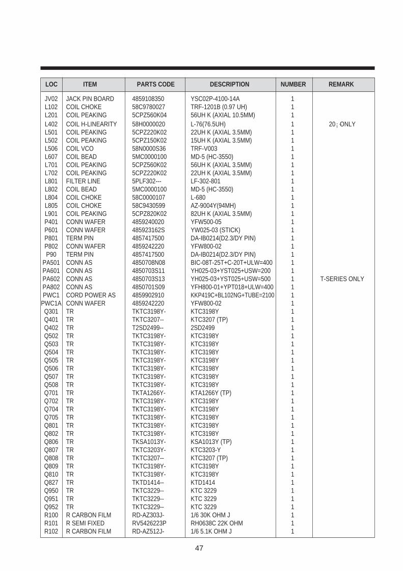
JV02 JACK PIN BOARD 4859108350 YSC02P-4100-14A 1L102 COIL CHOKE 58C9780027 TRF-1201B (0.97 UH) 1L201 COIL PEAKING 5CPZ560K04 56UH K (AXIAL 10.5MM) 1L402 COIL H-LINEARITY 58H0000020 L-76(76.5UH) 1 20¡–ONLYL501 COIL PEAKING 5CPZ220K02 22UH K (AXIAL 3.5MM) 1L502 COIL PEAKING 5CPZ150K02 15UH K (AXIAL 3.5MM) 1L506 COIL VCO 58N0000S36 TRF-V003 1L607 COIL BEAD 5MC0000100 MD-5 (HC-3550) 1L701 COIL PEAKING 5CPZ560K02 56UH K (AXIAL 3.5MM) 1L702 COIL PEAKING 5CPZ220K02 22UH K (AXIAL 3.5MM) 1L801 FILTER LINE 5PLF302--- LF-302-801 1L802 COIL BEAD 5MC0000100 MD-5 (HC-3550) 1L804 COIL CHOKE 58C0000107 L-680 1L805 COIL CHOKE 58C9430599 AZ-9004Y(94MH) 1L901 COIL PEAKING 5CPZ820K02 82UH K (AXIAL 3.5MM) 1P401 CONN WAFER 4859240020 YFW500-05 1P601 CONN WAFER 485923162S YW025-03 (STICK) 1P801 TERM PIN 4857417500 DA-IB0214(D2.3/DY PIN) 1P802 CONN WAFER 4859242220 YFW800-02 1P90 TERM PIN 4857417500 DA-IB0214(D2.3/DY PIN) 1
PA501 CONN AS 4850708N08 BIC-08T-25T+C-20T+ULW=400 1PA601 CONN AS 4850703S11 YH025-03+YST025+USW=200 1PA602 CONN AS 4850703S13 YH025-03+YST025+USW=500 1 T-SERIES ONLYPA802 CONN AS 4850701S09 YFH800-01+YPT018+ULW=400 1PWC1 CORD POWER AS 4859902910 KKP419C+BL102NG+TUBE=2100 1
PWC1A CONN WAFER 4859242220 YFW800-02 1Q301 TR TKTC3198Y- KTC3198Y 1Q401 TR TKTC3207-- KTC3207 (TP) 1Q402 TR T2SD2499-- 2SD2499 1Q502 TR TKTC3198Y- KTC3198Y 1Q503 TR TKTC3198Y- KTC3198Y 1Q504 TR TKTC3198Y- KTC3198Y 1Q505 TR TKTC3198Y- KTC3198Y 1Q506 TR TKTC3198Y- KTC3198Y 1Q507 TR TKTC3198Y- KTC3198Y 1Q508 TR TKTC3198Y- KTC3198Y 1Q701 TR TKTA1266Y- KTA1266Y (TP) 1Q702 TR TKTC3198Y- KTC3198Y 1Q704 TR TKTC3198Y- KTC3198Y 1Q705 TR TKTC3198Y- KTC3198Y 1Q801 TR TKTC3198Y- KTC3198Y 1Q802 TR TKTC3198Y- KTC3198Y 1Q806 TR TKSA1013Y- KSA1013Y (TP) 1Q807 TR TKTC3203Y- KTC3203-Y 1Q808 TR TKTC3207-- KTC3207 (TP) 1Q809 TR TKTC3198Y- KTC3198Y 1Q810 TR TKTC3198Y- KTC3198Y 1Q827 TR TKTD1414-- KTD1414 1Q950 TR TKTC3229-- KTC 3229 1Q951 TR TKTC3229-- KTC 3229 1Q952 TR TKTC3229-- KTC 3229 1R100 R CARBON FILM RD-AZ303J- 1/6 30K OHM J 1R101 R SEMI FIXED RV5426223P RH0638C 22K OHM 1R102 R CARBON FILM RD-AZ512J- 1/6 5.1K OHM J 1

48
LOC ITEM PARTS CODE DESCRIPTION NUMBER REMARK
R108 R CARBON FILM RD-AZ823J- 1/6 82K OHM J 1R109 R CARBON FILM RD-2Z820J- 1/2 82 OHM J 1R111 R CARBON FILM RD-AZ331J- 1/6 330 OHM J 1R113 R CARBON FILM RD-AZ102J- 1/6 1K OHM J 1R201 R FUSIBLE RF01Z229J- 1W 2.2 OHM J (TAPPING) 1R202 R M-OXIDE FILM RS01Z479J- 1W 4.7 OHM J (TAPPING) 1R203 R M-OXIDE FILM RS02Z240JS 2W 24 0HM J SMALL 1R206 R M-OXIDE FILM RS02Z273JS 2W 27K OHM J SMALL 1R301 R SEMI FIXED RV5426223P RH0638C 22K OHM 1R302 R SEMI FIXED RV5426472P RH0638C 4.7K OHM B 1R303 R CARBON FILM RD-AZ683J- 1/6 68K OHM J 1R304 R CARBON FILM RD-AZ393J- 1/6 39K OHM J 1R305 R CARBON FILM RD-AZ273J- 1/6 27K OHM J 1R306 R CARBON FILM RD-AZ183J- 1/6 18K OHM J 1R307 R CARBON FILM RD-AZ562J- 1/6 5.6K OHM J 1R308 R CARBON FILM RD-AZ473J- 1/6 47K OHM J 1R309 R CARBON FILM RD-AZ561J- 1/6 560 OHM J 1R310 R CARBON FILM RD-2Z331J- 1/2 330 OHM J 1R312 R M-OXIDE FILM RS01Z331J- 1W 330 OHM J (TAPPING) 1R313 R CARBON FILM RD-2Z229J- 1/2 2.2 OHM J 1R315 R CARBON FILM RD-AZ222J- 1/6 2.2K OHM J 1R316 R CARBON FILM RD-AZ202J- 1/6 2K OHM J 1R317 R CARBON FILM RD-AZ243J- 1/6 24K OHM J 1R318 R FUSIBLE RF01Z309J- 1W 3 OHM J (TAPPING) 1R401 R CARBON FILM RD-AZ561J- 1/6 560 OHM J 1R402 R M-OXIDE FILM RS02Z153JS 2W 15K OHM J SMALL 1R404 R CARBON FILM RD-4Z272J- 1/4 2.7K OHM J 1R405 R M-OXIDE FILM RS02Z512JS 2W 5.1K OHM J SMALL 1R406 R CARBON FILM RD-2Z154J- 1/2 150K OHM J 1 14¡–ONLY
RD-2Z124J- 1/2 120K OHM J 1 20¡–ONLYR407 R CARBON FILM RD-AZ102J- 1/6 1K OHM J 1R408 R M-OXIDE FILM RS01Z102J- 1W 1K OHM J (TAPPING) 1 20¡–ONLYR409 R CARBON FILM RD-2Z153J- 1/2 15K OHM J 1R410 R M-OXIDE FILM RS02Z512JS 2W 5.1K OHM J SMALL 1R411 R CARBON FILM RD-4Z303J- 1/4 30K OHM J 1R413 R M-OXIDE FILM RS02Z153JS 2W 15K OHM J SMALL 1R414 R M-OXIDE FILM RS02Z153JS 2W 15K OHM J SMALL 1R420 R CARBON FILM RD-4Z392J- 1/4 3.9K OHM J 1R501 R SEMI FIXED RV5426103P RH0638C 10K OHM B 1R503 R CARBON FILM RD-AZ103J- 1/6 10K OHM J 1R504 R CARBON FILM RD-AZ752J- 1/6 7.5K OHM J 1R505 R CARBON FILM RD-AZ103J- 1/6 10K OHM J 1R506 R CARBON FILM RD-AZ472J- 1/6 4.7K OHM J 1R507 R CARBON FILM RD-AZ472J- 1/6 4.7K OHM J 1R514 R CARBON FILM RD-AZ102J- 1/6 1K OHM J 1R517 R CARBON FILM RD-AZ391J- 1/6 390 OHM J 1R519 R CARBON FILM RD-AZ433J- 1/6 43K OHM J 1R520 R CARBON FILM RD-AZ154J- 1/6 150K OHM J 1R525 R CARBON FILM RD-AZ471J- 1/6 470 OHM J 1R527 R CARBON FILM RD-AZ331J- 1/6 330 OHM J 1R528 R CARBON FILM RD-AZ561J- 1/6 560 OHM J 1R531 R CARBON FILM RD-AZ102J- 1/6 1K OHM J 1R532 R CARBON FILM RD-AZ332J- 1/6 3.3K OHM J 1R533 R CARBON FILM RD-AZ103J- 1/6 10K OHM J 1

49
LOC ITEM PARTS CODE DESCRIPTION NUMBER REMARK
R535 R CARBON FILM RD-AZ823J- 1/6 82K OHM J 1R538 R CARBON FILM RD-AZ331J- 1/6 330 OHM J 1R539 R CARBON FILM RD-AZ332J- 1/6 3.3K OHM J 1R540 R SEMI FIXED RV5426103P RH0638C 10K OHM B 1R541 R CARBON FILM RD-AZ102J- 1/6 1K OHM J 1R543 R CARBON FILM RD-AZ203J- 1/6 20K OHM J 1R544 R CARBON FILM RD-AZ103J- 1/6 10K OHM J 1R546 R CARBON FILM RD-AZ103J- 1/6 10K OHM J 1R547 R CARBON FILM RD-AZ684J- 1/6 680K OHM J 1R548 R CARBON FILM RD-AZ202J- 1/6 2K OHM J 1R549 R CARBON FILM RD-AZ222J- 1/6 2.2K OHM J 1R551 R CARBON FILM RD-AZ103J- 1/6 10K OHM J 1R552 R CARBON FILM RD-AZ223J- 1/6 22K OHM J 1R553 R CARBON FILM RD-AZ473J- 1/6 47K OHM J 1R554 R CARBON FILM RD-AZ473J- 1/6 47K OHM J 1R555 R CARBON FILM RD-AZ332J- 1/6 3.3K OHM J 1R556 R CARBON FILM RD-AZ133J- 1/6 13K OHM J 1R557 R CARBON FILM RD-AZ243J- 1/6 24K OHM J 1R558 R CARBON FILM RD-AZ335J- 1/6 3.3M OHM J 1R559 R CARBON FILM RD-AZ335J- 1/6 3.3M OHM J 1R560 R CARBON FILM RD-AZ102J- 1/6 1K OHM J 1R561 R CARBON FILM RD-AZ473J- 1/6 47K OHM J 1R562 R CARBON FILM RD-AZ223J- 1/6 22K OHM J 1R563 R CARBON FILM RD-AZ103J- 1/6 10K OHM J 1R565 R CARBON FILM RD-AZ151J- 1/6 150 OHM J 1R566 R CARBON FILM RD-AZ151J- 1/6 150 OHM J 1R567 R CARBON FILM RD-AZ151J- 1/6 150 OHM J 1R580 R CARBON FILM RD-AZ202J- 1/6 2K OHM J 1R581 R CARBON FILM RD-AZ472J- 1/6 4.7K OHM J 1R582 R CARBON FILM RD-AZ103J- 1/6 10K OHM J 1R583 R CARBON FILM RD-AZ103J- 1/6 10K OHM J 1R584 R CARBON FILM RD-AZ473J- 1/6 47K OHM J 1R585 R CARBON FILM RD-4Z241J- 1/4 240 OHM J 1R587 R CARBON FILM RD-AZ561J- 1/6 560 OHM J 1R602 R CARBON FILM RD-AZ512J- 1/6 5.1K OHM J 1R603 R CARBON FILM RD-AZ512J- 1/6 5.1K OHM J 1R605 R CARBON FILM RD-2Z271J- 1/2 270 OHM J 1R606 R FUSIBLE RF01Z109J- 1W 1 OHM J (TAPPING) 1R701 R CARBON FILM RD-2Z241J- 1/2 240 OHM J 1R702 R CARBON FILM RD-AZ473J- 1/6 47K OHM J 1R703 R CARBON FILM RD-AZ473J- 1/6 47K OHM J 1R704 R CARBON FILM RD-AZ473J- 1/6 47K OHM J 1R705 R CARBON FILM RD-AZ101J- 1/6 100 OHM J 1R706 R CARBON FILM RD-AZ103J- 1/6 10K OHM J 1R707 R CARBON FILM RD-AZ101J- 1/6 100 OHM J 1R708 R CARBON FILM RD-AZ102J- 1/6 1K OHM J 1R709 R CARBON FILM RD-AZ102J- 1/6 1K OHM J 1R711 R CARBON FILM RD-AZ103J- 1/6 10K OHM J 1R712 R CARBON FILM RD-AZ103J- 1/6 10K OHM J 1R713 R CARBON FILM RD-AZ103J- 1/6 10K OHM J 1R714 R CARBON FILM RD-AZ471J- 1/6 470 OHM J 1R715 R CARBON FILM RD-AZ392J- 1/6 3.9K OHM J 1R716 R CARBON FILM RD-AZ102J- 1/6 1K OHM J 1R717 R CARBON FILM RD-AZ472J- 1/6 4.7K OHM J 1
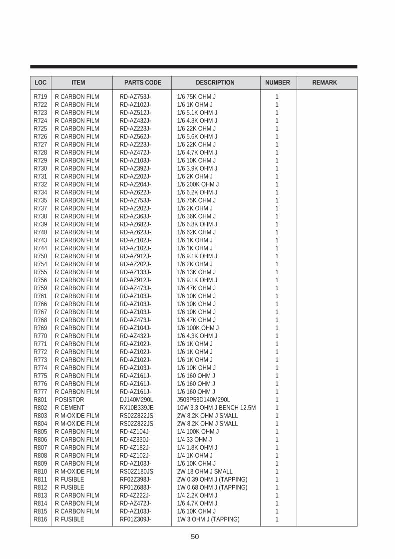
50
LOC ITEM PARTS CODE DESCRIPTION NUMBER REMARK
R719 R CARBON FILM RD-AZ753J- 1/6 75K OHM J 1R722 R CARBON FILM RD-AZ102J- 1/6 1K OHM J 1R723 R CARBON FILM RD-AZ512J- 1/6 5.1K OHM J 1R724 R CARBON FILM RD-AZ432J- 1/6 4.3K OHM J 1R725 R CARBON FILM RD-AZ223J- 1/6 22K OHM J 1R726 R CARBON FILM RD-AZ562J- 1/6 5.6K OHM J 1R727 R CARBON FILM RD-AZ223J- 1/6 22K OHM J 1R728 R CARBON FILM RD-AZ472J- 1/6 4.7K OHM J 1R729 R CARBON FILM RD-AZ103J- 1/6 10K OHM J 1R730 R CARBON FILM RD-AZ392J- 1/6 3.9K OHM J 1R731 R CARBON FILM RD-AZ202J- 1/6 2K OHM J 1R732 R CARBON FILM RD-AZ204J- 1/6 200K OHM J 1R734 R CARBON FILM RD-AZ622J- 1/6 6.2K OHM J 1R735 R CARBON FILM RD-AZ753J- 1/6 75K OHM J 1R737 R CARBON FILM RD-AZ202J- 1/6 2K OHM J 1R738 R CARBON FILM RD-AZ363J- 1/6 36K OHM J 1R739 R CARBON FILM RD-AZ682J- 1/6 6.8K OHM J 1R740 R CARBON FILM RD-AZ623J- 1/6 62K OHM J 1R743 R CARBON FILM RD-AZ102J- 1/6 1K OHM J 1R744 R CARBON FILM RD-AZ102J- 1/6 1K OHM J 1R750 R CARBON FILM RD-AZ912J- 1/6 9.1K OHM J 1R754 R CARBON FILM RD-AZ202J- 1/6 2K OHM J 1R755 R CARBON FILM RD-AZ133J- 1/6 13K OHM J 1R756 R CARBON FILM RD-AZ912J- 1/6 9.1K OHM J 1R759 R CARBON FILM RD-AZ473J- 1/6 47K OHM J 1R761 R CARBON FILM RD-AZ103J- 1/6 10K OHM J 1R766 R CARBON FILM RD-AZ103J- 1/6 10K OHM J 1R767 R CARBON FILM RD-AZ103J- 1/6 10K OHM J 1R768 R CARBON FILM RD-AZ473J- 1/6 47K OHM J 1R769 R CARBON FILM RD-AZ104J- 1/6 100K OHM J 1R770 R CARBON FILM RD-AZ432J- 1/6 4.3K OHM J 1R771 R CARBON FILM RD-AZ102J- 1/6 1K OHM J 1R772 R CARBON FILM RD-AZ102J- 1/6 1K OHM J 1R773 R CARBON FILM RD-AZ102J- 1/6 1K OHM J 1R774 R CARBON FILM RD-AZ103J- 1/6 10K OHM J 1R775 R CARBON FILM RD-AZ161J- 1/6 160 OHM J 1R776 R CARBON FILM RD-AZ161J- 1/6 160 OHM J 1R777 R CARBON FILM RD-AZ161J- 1/6 160 OHM J 1R801 POSISTOR DJ140M290L J503P53D140M290L 1R802 R CEMENT RX10B339JE 10W 3.3 OHM J BENCH 12.5M 1R803 R M-OXIDE FILM RS02Z822JS 2W 8.2K OHM J SMALL 1R804 R M-OXIDE FILM RS02Z822JS 2W 8.2K OHM J SMALL 1R805 R CARBON FILM RD-4Z104J- 1/4 100K OHM J 1R806 R CARBON FILM RD-4Z330J- 1/4 33 OHM J 1R807 R CARBON FILM RD-4Z182J- 1/4 1.8K OHM J 1R808 R CARBON FILM RD-4Z102J- 1/4 1K OHM J 1R809 R CARBON FILM RD-AZ103J- 1/6 10K OHM J 1R810 R M-OXIDE FILM RS02Z180JS 2W 18 OHM J SMALL 1R811 R FUSIBLE RF02Z398J- 2W 0.39 OHM J (TAPPING) 1R812 R FUSIBLE RF01Z688J- 1W 0.68 OHM J (TAPPING) 1R813 R CARBON FILM RD-4Z222J- 1/4 2.2K OHM J 1R814 R CARBON FILM RD-AZ472J- 1/6 4.7K OHM J 1R815 R CARBON FILM RD-AZ103J- 1/6 10K OHM J 1R816 R FUSIBLE RF01Z309J- 1W 3 OHM J (TAPPING) 1

51
LOC ITEM PARTS CODE DESCRIPTION NUMBER REMARK
R817 R FUSIBLE RF01Z369J- 1W 3.6 OHM J (TAPPING) 1 14¡–ONLYRF01Z399J- 1W 3.9 OHM J (TAPPING) 1 20¡–ONLY
R818 R CARBON FILM RD-AZ472J- 1/6 4.7K OHM J 1R820 R CARBON FILM RD-4Z223J- 1/4 22K OHM J 1R821 R FUSIBLE RF01Z688J- 1W 0.68 OHM J (TAPPING) 1R822 R CARBON FILM RD-4Z203J- 1/4 20K OHM J 1R823 R CARBON FILM RD-AZ822J- 1/6 8.2K OHM J 1R824 R CARBON FILM RD-4Z223J- 1/4 22K OHM J 1R825 R CARBON COMP RC-2Z275J- 1/2 2.7M OHM J 1R826 R CARBON COMP RC-2Z275J- 1/2 2.7M OHM J 1R827 R CARBON FILM RD-4Z103J- 1/4 10K OHM J 1R828 R CARBON FILM RD-4Z470J- 1/4 47 OHM J 1R829 R CARBON FILM RD-AZ103J- 1/6 10K OHM J 1R830 R CARBON FILM RD-AZ102J- 1/6 1K OHM J 1R831 R CARBON FILM RD-AZ103J- 1/6 10K OHM J 1R832 R CARBON FILM RD-4Z680J- 1/4 68 OHM J 1R833 R CARBON FILM RD-4Z101J- 1/4 100 OHM J 1R834 R CARBON FILM RD-4Z102J- 1/4 1K OHM J 1R835 R CARBON FILM RD-AZ152J- 1/6 1.5K OHM J 1R836 R CARBON FILM RD-AZ102J- 1/6 1K OHM J 1R950 R CARBON FILM RD-AZ151J- 1/6 150 OHM J 1R951 R M-OXIDE FILM RS02Z123JS 2W 12K 0HM J SMALL 1R952 R M-OXIDE FILM RS02Z123JS 2W 12K 0HM J SMALL 1R953 R M-OXIDE FILM RS02Z123JS 2W 12K 0HM J SMALL 1R954 R CARBON FILM RD-AZ151J- 1/6 150 OHM J 1R955 R CARBON FILM RD-AZ151J- 1/6 150 OHM J 1R956 R CARBON FILM RD-AZ151J- 1/6 150 OHM J 1R957 R CARBON FILM RD-2Z332J- 1/2 3.3K OHM J 1R958 R CARBON FILM RD-2Z332J- 1/2 3.3K OHM J 1R959 R CARBON FILM RD-2Z332J- 1/2 3.3K OHM J 1R961 R CARBON FILM RD-AZ152J- 1/6 1.5K OHM J 1R962 R CARBON FILM RD-AZ241J- 1/6 240 OHM J 1R963 R CARBON FILM RD-AZ560J- 1/6 56 OHM J 1R964 R CARBON FILM RD-AZ101J- 1/6 100 OHM J 1R965 R CARBON FILM RD-AZ152J- 1/6 1.5K OHM J 1R966 R CARBON FILM RD-AZ241J- 1/6 240 OHM J 1R967 R CARBON FILM RD-AZ560J- 1/6 56 OHM J 1R968 R CARBON FILM RD-AZ101J- 1/6 100 OHM J 1R969 R CARBON FILM RD-AZ152J- 1/6 1.5K OHM J 1R970 R CARBON FILM RD-AZ241J- 1/6 240 OHM J 1R971 R CARBON FILM RD-AZ560J- 1/6 56 OHM J 1R972 R CARBON FILM RD-AZ201J- 1/6 200 OHM J 1R981 R SEMI FIXED RV4121103P NVZ6THT 10K OHM 1R982 R SEMI FIXED RV4121103P NVZ6THT 10K OHM 1R983 R SEMI FIXED RV4121103P NVZ6THT 10K OHM 1R984 R SEMI FIXED RV4121201P NVZ6THT 200 OHM 1R985 R SEMI FIXED RV4121201P NVZ6THT 200 OHM 1RA01 R CARBON FILM RD-AZ102J- 1/6 1K OHM J 1RA02 R CARBON FILM RD-AZ822J- 1/6 8.2K OHM J 1RL01 SW RELAY 5SC0101003 DG12D1-0(M)-II 1C-1P 1RV01 R CARBON FILM RD-AZ750J- 1/6 75 OHM J 1RV02 R CARBON FILM RD-AZ101J- 1/6 100 OHM J 1SCT1 SOCKET CRT 4859302730 1SM-01S 1 14¡–ONLY
4859302530 1SM-03S 1 20¡–ONLY
52
LOC ITEM PARTS CODE DESCRIPTION NUMBER REMARK
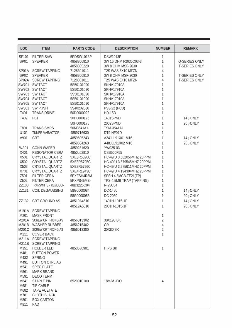
SF101 FILTER SAW 5PDSW1013P DSW1013P 1SP01 SPEAKER 4858306810 3W 16 OHM F2035C03-3 1 Q-SERIES ONLY
4858305220 3W 8 OHM MSF-2030 1 T-SERIES ONLYSP01A SCREW TAPPING 7128301011 T2S WAS 3X10 MFZN 4SP02 SPEAKER 4858306810 3W 8 OHM MSF-2030 1 T-SERIES ONLY
SP02A SCREW TAPPING 7128301011 T2S WAS 3X10 MFZN 4 T-SERIES ONLY SW701 SW TACT 5S50101090 SKHV17910A 1SW702 SW TACT 5S50101090 SKHV17910A 1SW703 SW TACT 5S50101090 SKHV17910A 1SW704 SW TACT 5S50101090 SKHV17910A 1SW705 SW TACT 5S50101090 SKHV17910A 1SW801 SW PUSH 5S40202080 PS3-22 (PCB) 1T401 TRANS DRIVE 50D0000022 HD-15D 1T402 FBT 50H0000176 1401SPND 1 14¡–ONLY
50H0000175 2002SPND 1 20¡–ONLYT801 TRANS SMPS 50M3541A1- TSM-3541A1 1U101 TUNER VARACTOR 4859716630 DT9-NF07D 1V901 CRT 4859605243 A34JLL91X01 M16 1 14¡–ONLY
4859604263 A48JLL91X02 M16 1 20¡–ONLYWA01 CONN WAFER 4859231620 YW025-03 1X401 RESONATOR CERA 4850L02810 CSB500F55 1X501 CRYSTAL QUARTZ 5XE3R5820C HC-49/U 3.582056MHZ 20PPM 1X502 CRYSTAL QUARTZ 5XE3R5795C HC-49/U 3.579545MHZ 20PPM 1X503 CRYSTAL QUARTZ 5XE3R5756C HC-49/U 3.575611MHZ 20PPM 1X701 CRYSTAL QUARTZ 5XE4R1943C HC-49/U 4.194304MHZ 20PPM 1Z501 FILTER CERA 5PXFSH4R5M SFSH 4.5MCB-TF21(TP) 1Z502 FILTER CERA 5PXPS45MB- TPS-4.5MB TRAP (TAPPING) 1
ZZ100 TRANSMITTER REMOCON 48B3225C04 R-25C04 1ZZ131 COIL DEGAUSSING 58G0000084 DC-1450 1 14¡–ONLY
58G0000086 DC-2050 1 20¡–ONLYZZ132 CRT GROUND AS 48519A4610 1401H-1015-1P 1 14¡–ONLY
48519A5010 2001H-1015-1P 1 20¡–ONLYM191A SCREW TAPPINGM201 MASK FRONT 1
M201A SCREW CRT FIXING AS 4856013302 30X190 BK 2M201B WASHER RUBBER 4856215402 CR 4M201C SCREW CRT FIXING AS 4856013300 30X80 BK 2M211 COVER BACK 1
M211A SCREW TAPPINGM211B SCREW TAPPINGM351 HOLDER LED 4853530901 HIPS BK 1M481 BUTTON POWERM482 SPRINGM491 BUTTON CTRL ASM541 SPEC PLATEM561 MARK BRANDM591 DECO TERMM641 STAPLE PIN 6520010100 18M/M JDO 4M681 TIE CABLEM682 TAPE ACETATEM781 CLOTH BLACKM801 BOX CARTONM811 PAD
53
LOC ITEM PARTS CODE DESCRIPTION NUMBER REMARK
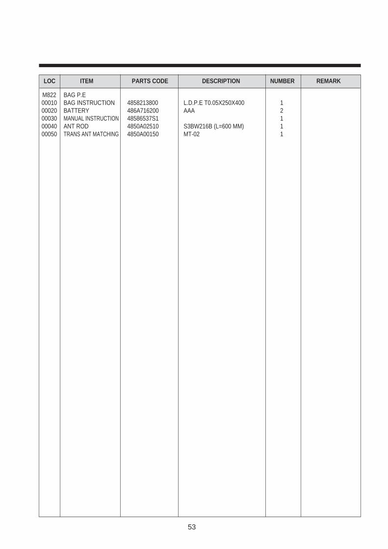
M822 BAG P.E00010 BAG INSTRUCTION 4858213800 L.D.P.E T0.05X250X400 100020 BATTERY 486A716200 AAA 200030 MANUAL INSTRUCTION 48586537S1 100040 ANT ROD 4850A02510 S3BW216B (L=600 MM) 100050 TRANS ANT MATCHING 4850A00150 MT-02 1


![Index of [diagramas.diagramasde.com] PHILIPS... · 2010. 8. 4. · Created Date: 4/3/20001:07:30 PM](https://img.pdfslide.us/doc/110x75/614234cb55c1d11d1b340b83/index-of-philips-2010-8-4-created-date-43200010730-pm.jpg)


![Untitled-30 [diagramas.diagramasde.com]diagramas.diagramasde.com/otros/DV-S525.pdf · Title: Untitled-30.max Author: GTeklewolde Created Date: 1/13/2003 12:35:30 PM](https://img.pdfslide.us/doc/110x75/5fbacd1c2af72c36b4713cec/untitled-30-title-untitled-30max-author-gteklewolde-created-date-1132003.jpg)