Embed Size (px)
Citation preview
May 2018 AN4439 Rev 2 1/16
1
AN4439Application note
L99ASC03G current sense amplifier offset adjust
Introduction
The L99ASC03G is a 3 phase BLDC motor controller. This device drives 6 MOSFETs for standard trapezoidal driven BLDC motors using back EMF for rotor position detection. This device has a current sense amplifier that provides an output of 1/2 Vcc (2.5 V) when there is no current sensed. This was done to provide bi-directional current detection. Some applications only need unidirectional current sensing. When this is the case, reducing or eliminating this offset would be advantageous to allow full use of the available microcontroller ADC range.
This application note provides the detailed calculations to provide the proper external resistor selection and tolerances required for optimal current sensing accuracy.
www.st.com
Contents AN4439
2/16 AN4439 Rev 2
Contents
1 The L99ASC03G current sense amplifier circuit . . . . . . . . . . . . . . . . . . 5
2 Calculating the input resistor values . . . . . . . . . . . . . . . . . . . . . . . . . . . 6
2.1 Calculating the transfer function from input to CSO . . . . . . . . . . . . . . . . . . 8
3 Generating a small offset to overcome input resistor tolerance and CSO lower limits 12
3.1 Bench evaluation . . . . . . . . . . . . . . . . . . . . . . . . . . . . . . . . . . . . . . . . . . . 13
3.2 Conclusion . . . . . . . . . . . . . . . . . . . . . . . . . . . . . . . . . . . . . . . . . . . . . . . . 14
4 Revision history . . . . . . . . . . . . . . . . . . . . . . . . . . . . . . . . . . . . . . . . . . . 15
AN4439 Rev 2 3/16
AN4439 List of tables
3
List of tables
Table 1. Rin values . . . . . . . . . . . . . . . . . . . . . . . . . . . . . . . . . . . . . . . . . . . . . . . . . . . . . . . . . . . . . . . 8Table 2. 1% Rin values for CSOmin=0.2 V. . . . . . . . . . . . . . . . . . . . . . . . . . . . . . . . . . . . . . . . . . . . 12Table 3. DC offset voltages with given resistor values . . . . . . . . . . . . . . . . . . . . . . . . . . . . . . . . . . . 13Table 4. Document revision history . . . . . . . . . . . . . . . . . . . . . . . . . . . . . . . . . . . . . . . . . . . . . . . . . 15
List of figures AN4439
4/16 AN4439 Rev 2
List of figures
Figure 1. L99ASC03G current sense amplifier circuit . . . . . . . . . . . . . . . . . . . . . . . . . . . . . . . . . . . . . 5Figure 2. L99ASC03G input offset circuit. . . . . . . . . . . . . . . . . . . . . . . . . . . . . . . . . . . . . . . . . . . . . . . 5Figure 3. Second stage Op-Amp . . . . . . . . . . . . . . . . . . . . . . . . . . . . . . . . . . . . . . . . . . . . . . . . . . . . . 6Figure 4. First stage Op-Amp. . . . . . . . . . . . . . . . . . . . . . . . . . . . . . . . . . . . . . . . . . . . . . . . . . . . . . . . 7Figure 5. CSO typical transfer functions at the 4 different gain settings . . . . . . . . . . . . . . . . . . . . . . . 9Figure 6. Transfer function tolerance at a gain of 20 . . . . . . . . . . . . . . . . . . . . . . . . . . . . . . . . . . . . . 10Figure 7. Transfer function tolerance at a gain of 100 . . . . . . . . . . . . . . . . . . . . . . . . . . . . . . . . . . . . 11Figure 8. DC offset at all inputs and gains . . . . . . . . . . . . . . . . . . . . . . . . . . . . . . . . . . . . . . . . . . . . . 11Figure 9. Inserted bias resistors for testing . . . . . . . . . . . . . . . . . . . . . . . . . . . . . . . . . . . . . . . . . . . . 13Figure 10. CSO vs. VIN at Av=20, calculated vs actual. . . . . . . . . . . . . . . . . . . . . . . . . . . . . . . . . . . . 14
AN4439 Rev 2 5/16
AN4439 The L99ASC03G current sense amplifier circuit
14
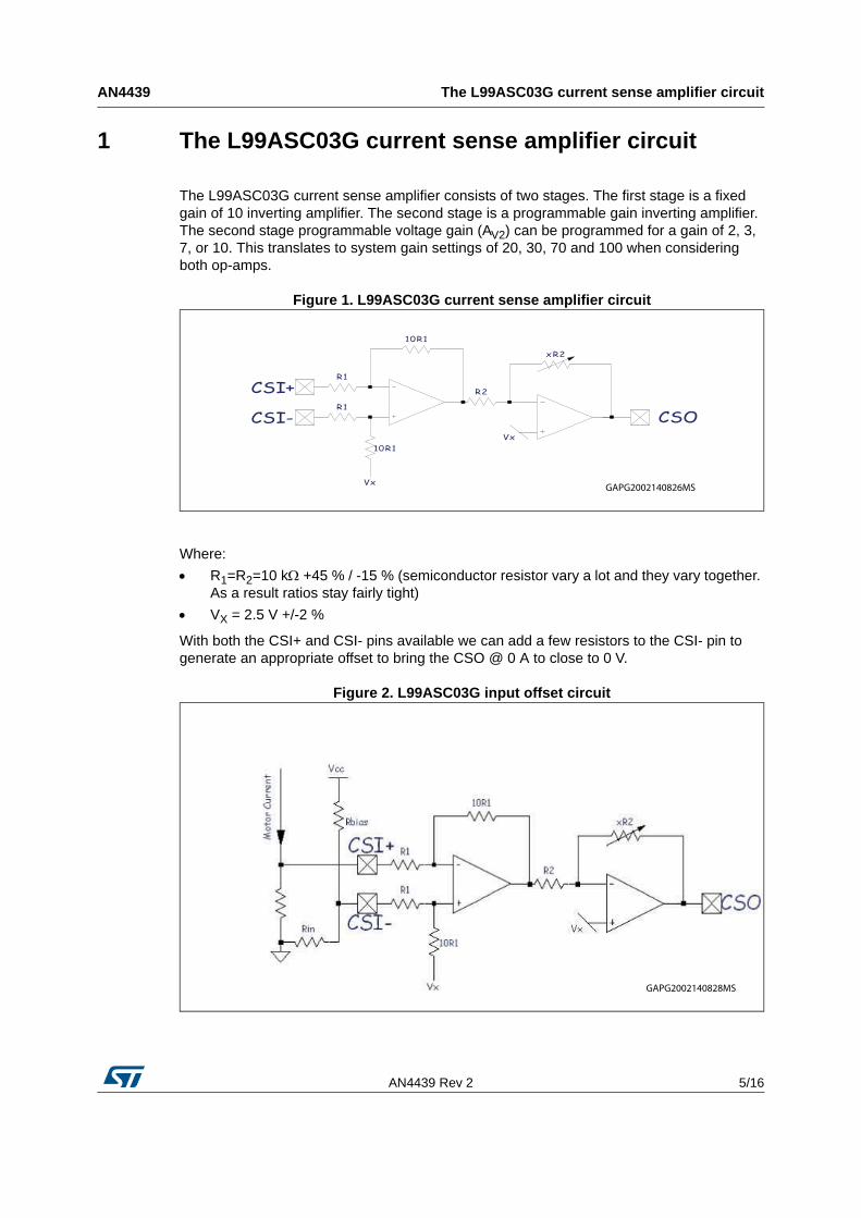
1 The L99ASC03G current sense amplifier circuit
The L99ASC03G current sense amplifier consists of two stages. The first stage is a fixed gain of 10 inverting amplifier. The second stage is a programmable gain inverting amplifier. The second stage programmable voltage gain (AV2) can be programmed for a gain of 2, 3, 7, or 10. This translates to system gain settings of 20, 30, 70 and 100 when considering both op-amps.
Figure 1. L99ASC03G current sense amplifier circuit
Where:
R1=R2=10 k +45 % / -15 % (semiconductor resistor vary a lot and they vary together. As a result ratios stay fairly tight)
VX = 2.5 V +/-2 %
With both the CSI+ and CSI- pins available we can add a few resistors to the CSI- pin to generate an appropriate offset to bring the CSO @ 0 A to close to 0 V.
Figure 2. L99ASC03G input offset circuit
GAPG2002140828MS
Calculating the input resistor values AN4439
6/16 AN4439 Rev 2
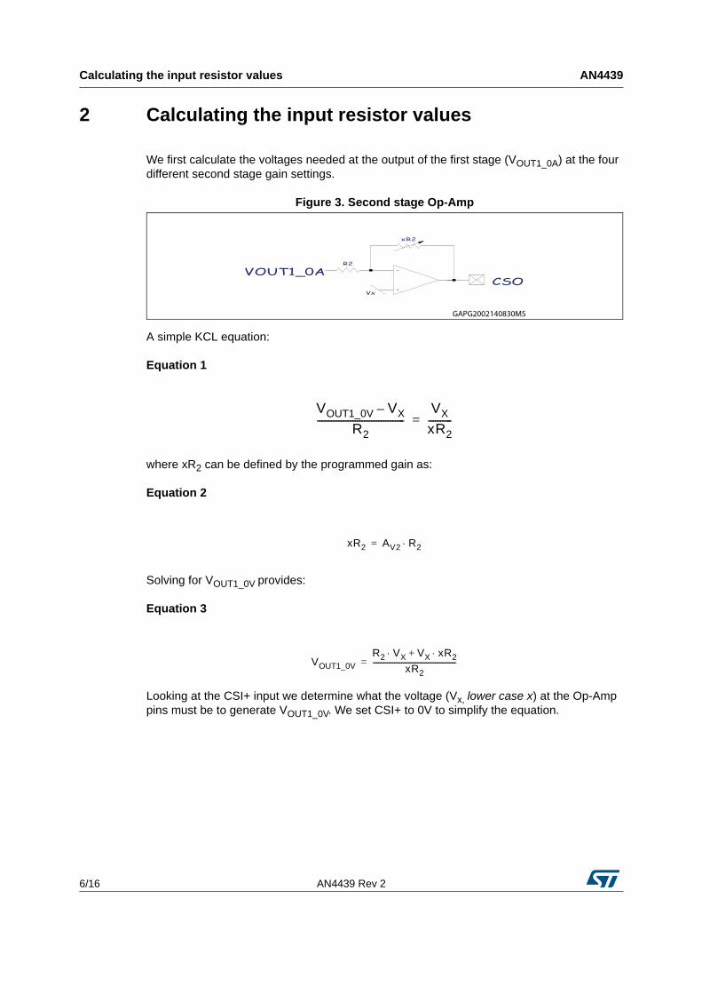
2 Calculating the input resistor values
We first calculate the voltages needed at the output of the first stage (VOUT1_0A) at the four different second stage gain settings.
Figure 3. Second stage Op-Amp
A simple KCL equation:
Equation 1
where xR2 can be defined by the programmed gain as:
Equation 2
Solving for VOUT1_0V provides:
Equation 3
Looking at the CSI+ input we determine what the voltage (Vx, lower case x) at the Op-Amp pins must be to generate VOUT1_0V. We set CSI+ to 0V to simplify the equation.
VOUT1_0V VX–
R2-------------------------------------
VX
xR2----------=
xR2 AV2 R2=
VOUT1_0V
R2 VX VX xR2+
xR2-----------------------------------------------=
AN4439 Rev 2 7/16
AN4439 Calculating the input resistor values
14
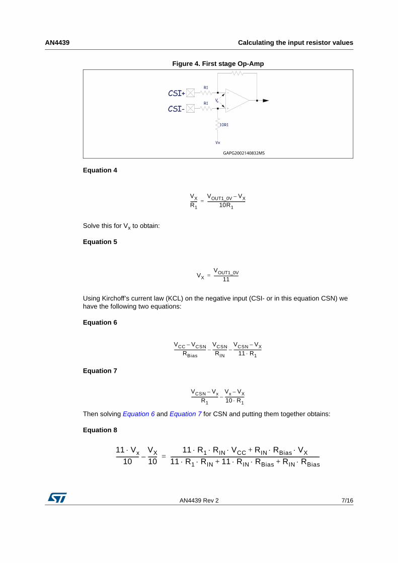
Figure 4. First stage Op-Amp
Equation 4
Solve this for Vx to obtain:
Equation 5
Using Kirchoff’s current law (KCL) on the negative input (CSI- or in this equation CSN) we have the following two equations:
Equation 6
Equation 7
Then solving Equation 6 and Equation 7 for CSN and putting them together obtains:
Equation 8
VX
R1-------
VOUT1_0V VX–
10R1--------------------------------------=
VX
VOUT1_0V
11------------------------=
VCC VCSN–
RBias--------------------------------
VCSN
RIN--------------–
VCSN VX–
11 R1----------------------------–
VCSN Vx–
R1---------------------------
Vx VX–
10 R1-------------------–
11 Vx10
-----------------VX
10-------–
11 R1 RIN VCC RIN RBias VX +
11 R1 RIN 11 R IN RBias RIN+ RBias +---------------------------------------------------------------------------------------------------------------=
Calculating the input resistor values AN4439
8/16 AN4439 Rev 2
Solving for RIN, while including Equation 2, Equation 3 and Equation 5 and simplifying we obtain:
Equation 9
We can now determine a value for RIN for a given RBias and gain setting.
For RBias=10 k1% and rounding to the nearest 1 % resistor value we have:
2.1 Calculating the transfer function from input to CSO
First we rewrite Equation 4 to include CSI+ (CSP) as a non-zero number:
Equation 10
We define Vx in terms of RIN, and RBias:
Equation 11
Defining VOUT1 in terms of VCSO:
Table 1. Rin values
Gain RIN (1%)
20 249
30 162
70 68.1
100 47.5
IN
11 R1 RBias VX 11 R1 VX RBias VX 110 AV2 R1 VCC – 10 AV2 RBias VX –+---------------------------------------------------------------------------------------------------------------------------------------------------------------------------------------=
VCSP Vx–
R1--------------------------
Vx VOUT1–
10 R1-----------------------------=
AN4439 Rev 2 9/16
AN4439 Calculating the input resistor values
14
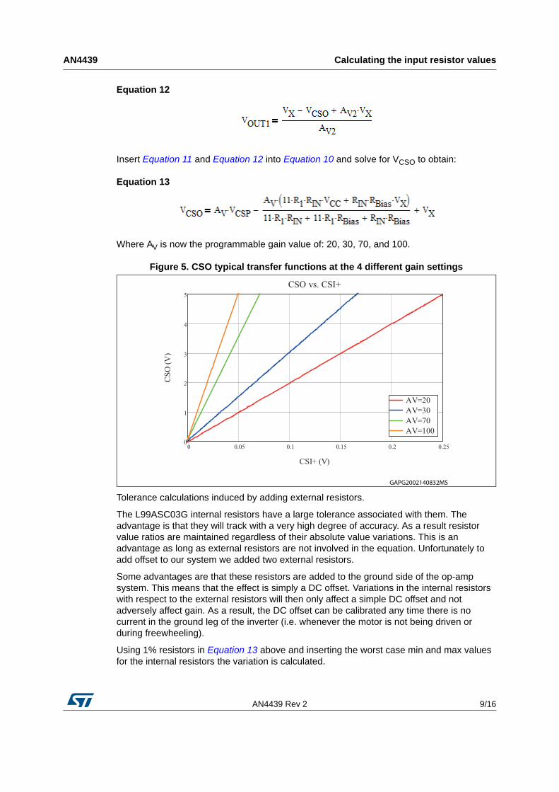
Equation 12
Insert Equation 11 and Equation 12 into Equation 10 and solve for VCSO to obtain:
Equation 13
Where AV is now the programmable gain value of: 20, 30, 70, and 100.
Figure 5. CSO typical transfer functions at the 4 different gain settings
Tolerance calculations induced by adding external resistors.
The L99ASC03G internal resistors have a large tolerance associated with them. The advantage is that they will track with a very high degree of accuracy. As a result resistor value ratios are maintained regardless of their absolute value variations. This is an advantage as long as external resistors are not involved in the equation. Unfortunately to add offset to our system we added two external resistors.
Some advantages are that these resistors are added to the ground side of the op-amp system. This means that the effect is simply a DC offset. Variations in the internal resistors with respect to the external resistors will then only affect a simple DC offset and not adversely affect gain. As a result, the DC offset can be calibrated any time there is no current in the ground leg of the inverter (i.e. whenever the motor is not being driven or during freewheeling).
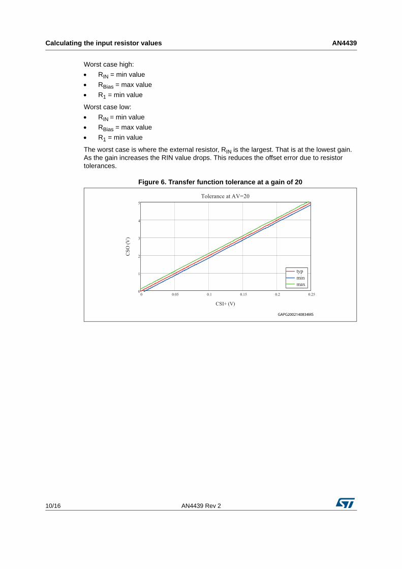
Using 1% resistors in Equation 13 above and inserting the worst case min and max values for the internal resistors the variation is calculated.
0 0.05 0.1 0.15 0.2 0.250
1
2
3
4
5
AV=20AV=30AV=70AV=100
CSO vs. CSI+
CSI+ (V)
CSO
(V)
GAPG2002140832MS
Calculating the input resistor values AN4439
10/16 AN4439 Rev 2
Worst case high:
RIN = min value
RBias = max value
R1 = min value
Worst case low:
RIN = min value
RBias = max value
R1 = min value
The worst case is where the external resistor, RIN is the largest. That is at the lowest gain. As the gain increases the RIN value drops. This reduces the offset error due to resistor tolerances.
Figure 6. Transfer function tolerance at a gain of 20
0 0.05 0.1 0.15 0.2 0.250
1
2
3
4
5
typminmax
Tolerance at AV=20
CSI+ (V)
CSO
(V)
GAPG2002140834MS
AN4439 Rev 2 11/16
AN4439 Calculating the input resistor values
14
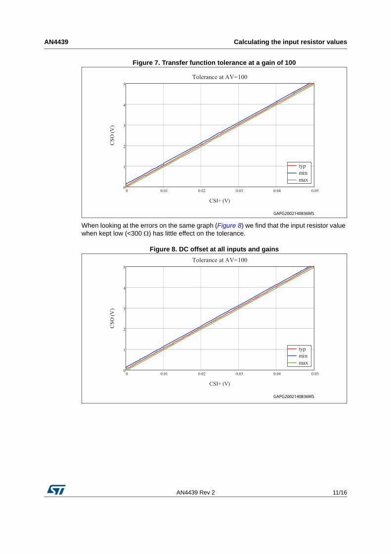
Figure 7. Transfer function tolerance at a gain of 100
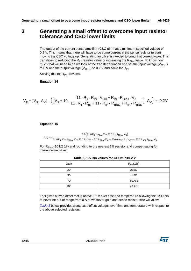
When looking at the errors on the same graph (Figure 8) we find that the input resistor value when kept low (<300 ) has little effect on the tolerance.
Figure 8. DC offset at all inputs and gains
0 0.01 0.02 0.03 0.04 0.050
1
2
3
4
5
typminmax
Tolerance at AV=100
CSI+ (V)
CSO
(V)
GAPG2002140836MS
0 0.01 0.02 0.03 0.04 0.050
1
2
3
4
5
typminmax
Tolerance at AV=100
CSI+ (V)
CSO
(V)
GAPG2002140836MS
Generating a small offset to overcome input resistor tolerance and CSO lower limits AN4439
12/16 AN4439 Rev 2
3 Generating a small offset to overcome input resistor tolerance and CSO lower limits
The output of the current sense amplifier (CSO pin) has a minimum specified voltage of 0.2 V. This means that there will have to be some current in the sense resistor to start moving the CSO voltage up. Generating an offset is needed to bring that current lower. This translates to reducing the RIN resistor value or increasing the RBias value. To know how much that will need to be we look at the transfer equation and set the input voltage (VCSI+) to 0 V and the output voltage (VCSO) to 0.2 V and solve for RIN.
Solving this for RIN provides:
Equation 14
Equation 15
For RBias=10 k1% and rounding to the nearest 1% resistor and compensating for tolerance we have:
This gives a fixed offset that is above 0.2 V over time and temperature allowing the CSO pin to never be out of range from 0 A to whatever gain and sense resistor size will allow.
Table 3 below provides worst case offset voltages over time and temperature with respect to the above selected resistors.
VX VX AV VX 1011 R1 RIN VCC RIN RBias VX +
11 R1 RIN 11 R IN RBias RIN+ RBias +---------------------------------------------------------------------------------------------------------------+
AV –+ 0.2V=
Table 2. 1% Rin values for CSOmin=0.2 V
Gain RIN (1%)
20 215
30 143
70 60.4
100 42.2
RIN
1.0 11.0 R1 RBias V 55.0 R1 RBias VX
11.0 R1 V RBias V 55.0 R1 VX 5.0 RBias VX 550.0AV2 R1 VCC 50.0 AV2 RBias VX
AN4439 Rev 2 13/16
AN4439 Generating a small offset to overcome input resistor tolerance and CSO lower limits
14
These voltages are worst case given the external and internal resistor tolerances. There is a small overlap that drops below the worst case 0.2 V CSO minimum voltage. The worst case difference is at the gain of 30 with a 0.012 V error. This translates to a very small sense current. If this is an issue the next 1% resistor value lower will improve this to above the 0.2 V threshold.
3.1 Bench evaluation
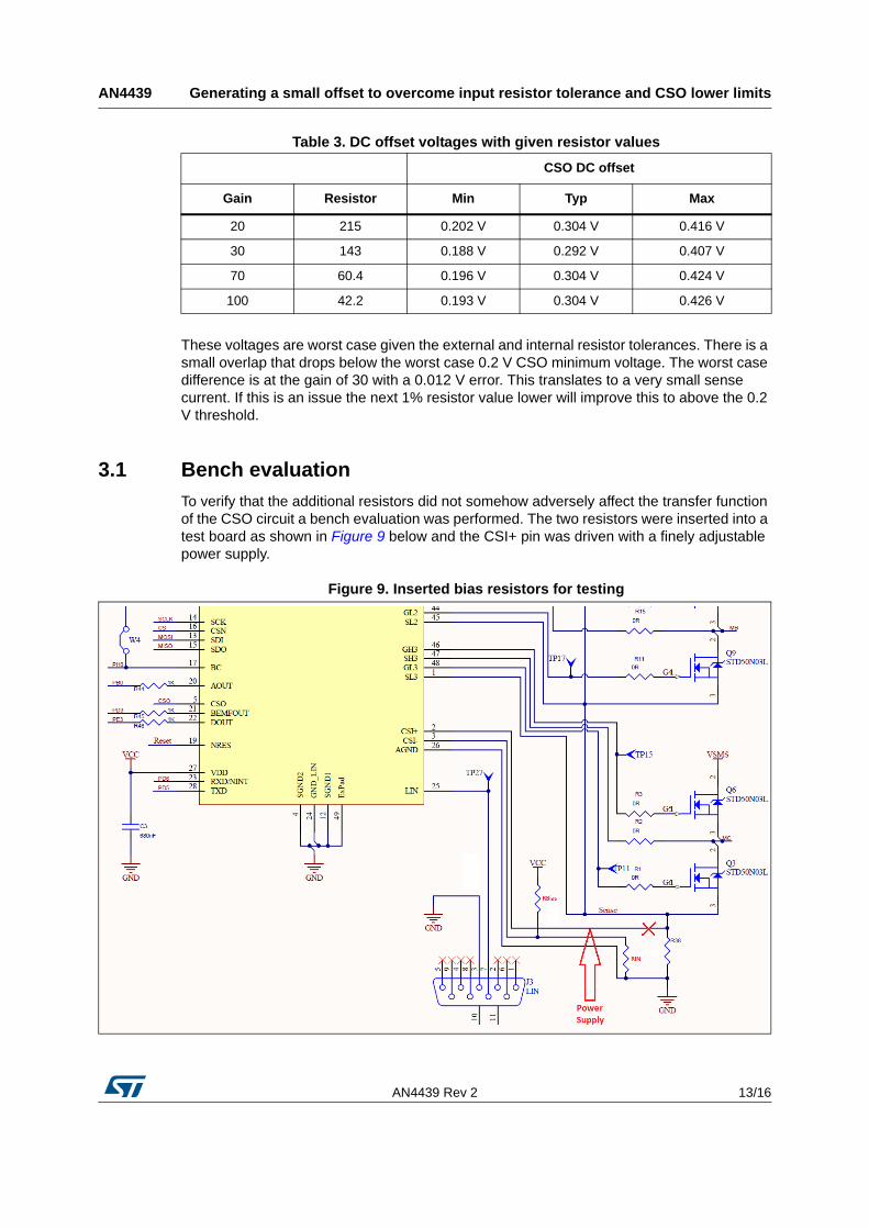
To verify that the additional resistors did not somehow adversely affect the transfer function of the CSO circuit a bench evaluation was performed. The two resistors were inserted into a test board as shown in Figure 9 below and the CSI+ pin was driven with a finely adjustable power supply.
Figure 9. Inserted bias resistors for testing
Table 3. DC offset voltages with given resistor values
CSO DC offset
Gain Resistor Min Typ Max
20 215 0.202 V 0.304 V 0.416 V
30 143 0.188 V 0.292 V 0.407 V
70 60.4 0.196 V 0.304 V 0.424 V
100 42.2 0.193 V 0.304 V 0.426 V
Generating a small offset to overcome input resistor tolerance and CSO lower limits AN4439
14/16 AN4439 Rev 2
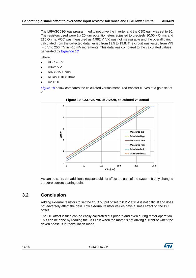
The L99ASC03G was programmed to not drive the inverter and the CSO gain was set to 20. The resistors used were 2 x 20 turn potentiometers adjusted to precisely 10.00 k Ohms and 215 Ohms. VCC was measured as 4.982 V. VX was not measurable and the overall gain, calculated from the collected data, varied from 19.5 to 19.8. The circuit was tested from VIN = 0 V to 250 mV in ~10 mV increments. This data was compared to the calculated values generated by Equation 13
where:
VCC = 5 V
VX=2.5 V
RIN=215 Ohms
RBias = 10 kOhms
Av = 20
Figure 10 below compares the calculated versus measured transfer curves at a gain set at 20.
Figure 10. CSO vs. VIN at Av=20, calculated vs actual
As can be seen, the additional resistors did not affect the gain of the system. It only changed the zero current starting point.
3.2 Conclusion
Adding external resistors to set the CSO output offset to 0.2 V at 0 A is not difficult and does not adversely affect the gain. Low external resistor values have a small effect on the DC offset.
The DC offset issues can be easily calibrated out prior to and even during motor operation. This can be done by reading the CSO pin when the motor is not driving current or when the driven phase is in recirculation mode.
0
1
2
3
4
5
0 50 100 150 200 250
CSO
(V)
CSI+ (mV)
Measured typ
Calculated typ
Measured min
Measured max
Calculated min
Calculated max
AN4439 Rev 2 15/16
AN4439 Revision history
15
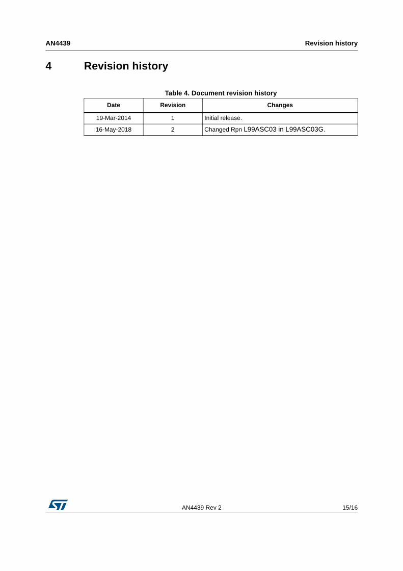
4 Revision history
Table 4. Document revision history
Date Revision Changes
19-Mar-2014 1 Initial release.
16-May-2018 2 Changed Rpn L99ASC03 in L99ASC03G.
AN4439
16/16 AN4439 Rev 2
IMPORTANT NOTICE – PLEASE READ CAREFULLY
STMicroelectronics NV and its subsidiaries (“ST”) reserve the right to make changes, corrections, enhancements, modifications, and improvements to ST products and/or to this document at any time without notice. Purchasers should obtain the latest relevant information on ST products before placing orders. ST products are sold pursuant to ST’s terms and conditions of sale in place at the time of order acknowledgement.
Purchasers are solely responsible for the choice, selection, and use of ST products and ST assumes no liability for application assistance or the design of Purchasers’ products.
No license, express or implied, to any intellectual property right is granted by ST herein.
Resale of ST products with provisions different from the information set forth herein shall void any warranty granted by ST for such product.
ST and the ST logo are trademarks of ST. All other product or service names are the property of their respective owners.
Information in this document supersedes and replaces information previously supplied in any prior versions of this document.
© 2018 STMicroelectronics – All rights reserved