Embed Size (px)
Citation preview

April 2015 DocID026442 Rev 2 1/47
AN4506Application note
L3GD20H: 3-axis digital output gyroscope
By Michele Ferraina
IntroductionThis document is intended to provide information on the use of, and application hints related to, ST’s L3GD20H 3-axis digital gyroscope.
The L3GD20H is a 3-axis angular rate sensor with a digital I2C/SPI serial interface standard output.
The device has a full scale of ±245/±500/±2000 dps and is capable of measuring rates with a user-selectable bandwidth.
The device may be configured to generate interrupt signals by detecting an independent wake-up event. Thresholds and timing of the interrupt generator are programmable by the end user on the fly.
The L3GD20H has an integrated 32-level first in first out (FIFO) buffer allowing the user to store data in order to limit intervention by the host processor.
The L3GD20H is available in a small thin plastic land grid array package (LGA-16 3x3x1) and it is guaranteed to operate over an extended temperature range from -40 °C to +85 °C.
The ultra-small size and weight of the SMD package make it an ideal choice for handheld portable applications such as smartphones, wearables or any other application where reduced package size and weight are required.
www.st.com
Contents AN4506
2/47 DocID026442 Rev 2
Contents
1 Registers . . . . . . . . . . . . . . . . . . . . . . . . . . . . . . . . . . . . . . . . . . . . . . . . . . 6
2 Operating modes . . . . . . . . . . . . . . . . . . . . . . . . . . . . . . . . . . . . . . . . . . . . 82.1 Power-down mode . . . . . . . . . . . . . . . . . . . . . . . . . . . . . . . . . . . . . . . . . . 10
2.2 Sleep mode . . . . . . . . . . . . . . . . . . . . . . . . . . . . . . . . . . . . . . . . . . . . . . . 10
2.3 Low ODR mode . . . . . . . . . . . . . . . . . . . . . . . . . . . . . . . . . . . . . . . . . . . . 10
2.4 Normal mode . . . . . . . . . . . . . . . . . . . . . . . . . . . . . . . . . . . . . . . . . . . . . . 10
2.5 Switching modes . . . . . . . . . . . . . . . . . . . . . . . . . . . . . . . . . . . . . . . . . . . 11
3 Reading angular rate data . . . . . . . . . . . . . . . . . . . . . . . . . . . . . . . . . . . 113.1 Startup sequence . . . . . . . . . . . . . . . . . . . . . . . . . . . . . . . . . . . . . . . . . . . 11
3.2 Using the status register . . . . . . . . . . . . . . . . . . . . . . . . . . . . . . . . . . . . . . 12
3.3 Using the data-ready (DRDY) signal . . . . . . . . . . . . . . . . . . . . . . . . . . . . 12
3.4 Using the block data update (BDU) feature . . . . . . . . . . . . . . . . . . . . . . . 13
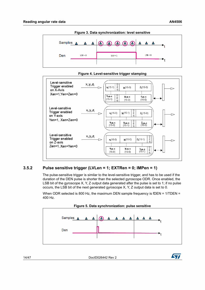
3.5 DEN function . . . . . . . . . . . . . . . . . . . . . . . . . . . . . . . . . . . . . . . . . . . . . . 133.5.1 Level-sensitive trigger stamping (LVLen = 1; EXTRen = 0; IMPen = 0) 13
3.5.2 Pulse sensitive trigger (LVLen = 1; EXTRen = 0; IMPen = 1) . . . . . . . . 14
3.5.3 Edge-sensitive trigger (LVLen = 0; EXTRen = 1; IMPen = 0) . . . . . . . . 15
3.6 Understanding angular rate data . . . . . . . . . . . . . . . . . . . . . . . . . . . . . . . 153.6.1 Data alignment . . . . . . . . . . . . . . . . . . . . . . . . . . . . . . . . . . . . . . . . . . . . 15
3.6.2 Big-little endian selection . . . . . . . . . . . . . . . . . . . . . . . . . . . . . . . . . . . . 15
3.6.3 Example of angular rate data . . . . . . . . . . . . . . . . . . . . . . . . . . . . . . . . . 16
4 Digital filters . . . . . . . . . . . . . . . . . . . . . . . . . . . . . . . . . . . . . . . . . . . . . . . 164.1 Filter configuration . . . . . . . . . . . . . . . . . . . . . . . . . . . . . . . . . . . . . . . . . . 17
4.2 Low-pass filters . . . . . . . . . . . . . . . . . . . . . . . . . . . . . . . . . . . . . . . . . . . . 18
4.3 High-pass filter . . . . . . . . . . . . . . . . . . . . . . . . . . . . . . . . . . . . . . . . . . . . . 194.3.1 Normal mode . . . . . . . . . . . . . . . . . . . . . . . . . . . . . . . . . . . . . . . . . . . . . 20
4.3.2 REFERENCE mode . . . . . . . . . . . . . . . . . . . . . . . . . . . . . . . . . . . . . . . . 20
4.3.3 Autoreset . . . . . . . . . . . . . . . . . . . . . . . . . . . . . . . . . . . . . . . . . . . . . . . . 21
5 Interrupt generation . . . . . . . . . . . . . . . . . . . . . . . . . . . . . . . . . . . . . . . . 215.1 Interrupt pin configuration . . . . . . . . . . . . . . . . . . . . . . . . . . . . . . . . . . . . . 22
AN4506 Contents
DocID026442 Rev 2 3/47
5.2 Interrupt configuration . . . . . . . . . . . . . . . . . . . . . . . . . . . . . . . . . . . . . . . 23
5.3 Threshold . . . . . . . . . . . . . . . . . . . . . . . . . . . . . . . . . . . . . . . . . . . . . . . . . 24
5.4 Duration . . . . . . . . . . . . . . . . . . . . . . . . . . . . . . . . . . . . . . . . . . . . . . . . . . 24
5.5 Selective axis movement and wake-up interrupts . . . . . . . . . . . . . . . . . . 275.5.1 Wake-up . . . . . . . . . . . . . . . . . . . . . . . . . . . . . . . . . . . . . . . . . . . . . . . . . 28
5.5.2 HP filter bypassed . . . . . . . . . . . . . . . . . . . . . . . . . . . . . . . . . . . . . . . . . 28
5.5.3 Using the HP filter . . . . . . . . . . . . . . . . . . . . . . . . . . . . . . . . . . . . . . . . . 29
5.6 Selective axis movement detection . . . . . . . . . . . . . . . . . . . . . . . . . . . . . 30
6 First-in first-out (FIFO) buffer . . . . . . . . . . . . . . . . . . . . . . . . . . . . . . . . . 326.1 FIFO description . . . . . . . . . . . . . . . . . . . . . . . . . . . . . . . . . . . . . . . . . . . . 32
6.2 FIFO registers . . . . . . . . . . . . . . . . . . . . . . . . . . . . . . . . . . . . . . . . . . . . . 336.2.1 Control register 5 (0x24) . . . . . . . . . . . . . . . . . . . . . . . . . . . . . . . . . . . . 33
6.2.2 FIFO control register (0x2E) . . . . . . . . . . . . . . . . . . . . . . . . . . . . . . . . . 34
6.2.3 FIFO source register (0x2F) . . . . . . . . . . . . . . . . . . . . . . . . . . . . . . . . . 35
6.3 FIFO modes . . . . . . . . . . . . . . . . . . . . . . . . . . . . . . . . . . . . . . . . . . . . . . . 366.3.1 Bypass mode . . . . . . . . . . . . . . . . . . . . . . . . . . . . . . . . . . . . . . . . . . . . . 36
6.3.2 FIFO mode . . . . . . . . . . . . . . . . . . . . . . . . . . . . . . . . . . . . . . . . . . . . . . . 36
6.3.3 Stream mode . . . . . . . . . . . . . . . . . . . . . . . . . . . . . . . . . . . . . . . . . . . . . 37
6.3.4 Dynamic Stream mode . . . . . . . . . . . . . . . . . . . . . . . . . . . . . . . . . . . . . 40
6.3.5 Stream-to-FIFO mode . . . . . . . . . . . . . . . . . . . . . . . . . . . . . . . . . . . . . . 41
6.3.6 Bypass-to-Stream mode . . . . . . . . . . . . . . . . . . . . . . . . . . . . . . . . . . . . 42
6.3.7 Bypass-to-FIFO mode . . . . . . . . . . . . . . . . . . . . . . . . . . . . . . . . . . . . . . 43
6.4 FIFO threshold . . . . . . . . . . . . . . . . . . . . . . . . . . . . . . . . . . . . . . . . . . . . . 44
6.5 Retrieving data from FIFO . . . . . . . . . . . . . . . . . . . . . . . . . . . . . . . . . . . . 45
7 Temperature sensor . . . . . . . . . . . . . . . . . . . . . . . . . . . . . . . . . . . . . . . . 46
8 Revision history . . . . . . . . . . . . . . . . . . . . . . . . . . . . . . . . . . . . . . . . . . . 46
List of tables AN4506
4/47 DocID026442 Rev 2
List of tables
Table 1. Registers. . . . . . . . . . . . . . . . . . . . . . . . . . . . . . . . . . . . . . . . . . . . . . . . . . . . . . . . . . . . . . . . 6Table 2. Operating mode selection. . . . . . . . . . . . . . . . . . . . . . . . . . . . . . . . . . . . . . . . . . . . . . . . . . . 8Table 3. Data rate configuration . . . . . . . . . . . . . . . . . . . . . . . . . . . . . . . . . . . . . . . . . . . . . . . . . . . . . 8Table 4. Power consumption . . . . . . . . . . . . . . . . . . . . . . . . . . . . . . . . . . . . . . . . . . . . . . . . . . . . . . 10Table 5. Turn-on time . . . . . . . . . . . . . . . . . . . . . . . . . . . . . . . . . . . . . . . . . . . . . . . . . . . . . . . . . . . . 11Table 6. DEN configurations. . . . . . . . . . . . . . . . . . . . . . . . . . . . . . . . . . . . . . . . . . . . . . . . . . . . . . . 13Table 7. Output data registers content vs. angular rate (FS = 245 dps). . . . . . . . . . . . . . . . . . . . . . 16Table 8. CTRL5 register . . . . . . . . . . . . . . . . . . . . . . . . . . . . . . . . . . . . . . . . . . . . . . . . . . . . . . . . . . 16Table 9. Out_Sel configuration setting . . . . . . . . . . . . . . . . . . . . . . . . . . . . . . . . . . . . . . . . . . . . . . . 17Table 10. IG_SEL configuration settings . . . . . . . . . . . . . . . . . . . . . . . . . . . . . . . . . . . . . . . . . . . . . . 17Table 11. Low-pass filter cutoff frequency . . . . . . . . . . . . . . . . . . . . . . . . . . . . . . . . . . . . . . . . . . . . . 18Table 12. CTRL2 register . . . . . . . . . . . . . . . . . . . . . . . . . . . . . . . . . . . . . . . . . . . . . . . . . . . . . . . . . . 19Table 13. High-pass filter cut-off frequencies [Hz] . . . . . . . . . . . . . . . . . . . . . . . . . . . . . . . . . . . . . . . 19Table 14. High-pass filter mode configuration . . . . . . . . . . . . . . . . . . . . . . . . . . . . . . . . . . . . . . . . . . 19Table 15. REFERENCE mode LSB value . . . . . . . . . . . . . . . . . . . . . . . . . . . . . . . . . . . . . . . . . . . . . 20Table 16. CTRL3 register . . . . . . . . . . . . . . . . . . . . . . . . . . . . . . . . . . . . . . . . . . . . . . . . . . . . . . . . . . 22Table 17. CTRL3 description . . . . . . . . . . . . . . . . . . . . . . . . . . . . . . . . . . . . . . . . . . . . . . . . . . . . . . . 22Table 18. IG_CFG register . . . . . . . . . . . . . . . . . . . . . . . . . . . . . . . . . . . . . . . . . . . . . . . . . . . . . . . . . 23Table 19. IG_CFG description . . . . . . . . . . . . . . . . . . . . . . . . . . . . . . . . . . . . . . . . . . . . . . . . . . . . . . 23Table 20. Interrupt mode configuration. . . . . . . . . . . . . . . . . . . . . . . . . . . . . . . . . . . . . . . . . . . . . . . . 23Table 21. IG_THS_xH register . . . . . . . . . . . . . . . . . . . . . . . . . . . . . . . . . . . . . . . . . . . . . . . . . . . . . . 24Table 22. IG_THS_xL register . . . . . . . . . . . . . . . . . . . . . . . . . . . . . . . . . . . . . . . . . . . . . . . . . . . . . . 24Table 23. Threshold LSB value. . . . . . . . . . . . . . . . . . . . . . . . . . . . . . . . . . . . . . . . . . . . . . . . . . . . . . 24Table 24. IG_DURATION register . . . . . . . . . . . . . . . . . . . . . . . . . . . . . . . . . . . . . . . . . . . . . . . . . . . 24Table 25. IG_DURATION description. . . . . . . . . . . . . . . . . . . . . . . . . . . . . . . . . . . . . . . . . . . . . . . . . 24Table 26. Duration LSB value in Normal mode. . . . . . . . . . . . . . . . . . . . . . . . . . . . . . . . . . . . . . . . . . 24Table 27. FIFO buffer full representation (32nd sample set stored) . . . . . . . . . . . . . . . . . . . . . . . . . . 32Table 28. FIFO overrun representation (33rd sample set stored and 1st sample discarded). . . . . . . 33Table 29. FIFO enable bit in CTRL5. . . . . . . . . . . . . . . . . . . . . . . . . . . . . . . . . . . . . . . . . . . . . . . . . . 33Table 30. FIFO_CTRL register . . . . . . . . . . . . . . . . . . . . . . . . . . . . . . . . . . . . . . . . . . . . . . . . . . . . . . 34Table 31. FIFO_SRC register . . . . . . . . . . . . . . . . . . . . . . . . . . . . . . . . . . . . . . . . . . . . . . . . . . . . . . . 35Table 32. FIFO_SRC_REG behavior assuming FTH[4:0] = 15 . . . . . . . . . . . . . . . . . . . . . . . . . . . . . 35Table 33. CTRL3 (0x22) . . . . . . . . . . . . . . . . . . . . . . . . . . . . . . . . . . . . . . . . . . . . . . . . . . . . . . . . . . . 35Table 34. Document revision history. . . . . . . . . . . . . . . . . . . . . . . . . . . . . . . . . . . . . . . . . . . . . . . . . . 46
AN4506 List of figures
DocID026442 Rev 2 5/47
List of figures
Figure 1. Low-pass filter transfer function . . . . . . . . . . . . . . . . . . . . . . . . . . . . . . . . . . . . . . . . . . . . . . 9Figure 2. Data-ready signal . . . . . . . . . . . . . . . . . . . . . . . . . . . . . . . . . . . . . . . . . . . . . . . . . . . . . . . . 13Figure 3. Data synchronization: level sensitive . . . . . . . . . . . . . . . . . . . . . . . . . . . . . . . . . . . . . . . . . 14Figure 4. Level-sensitive trigger stamping . . . . . . . . . . . . . . . . . . . . . . . . . . . . . . . . . . . . . . . . . . . . . 14Figure 5. Data synchronization: pulse sensitive. . . . . . . . . . . . . . . . . . . . . . . . . . . . . . . . . . . . . . . . . 14Figure 6. Data synchronization: edge sensitive . . . . . . . . . . . . . . . . . . . . . . . . . . . . . . . . . . . . . . . . . 15Figure 7. Low-pass/high-pass filter connections block diagram. . . . . . . . . . . . . . . . . . . . . . . . . . . . . 17Figure 8. High-pass filter reset by reading the REFERENCE register . . . . . . . . . . . . . . . . . . . . . . . . 20Figure 9. REFERENCE mode . . . . . . . . . . . . . . . . . . . . . . . . . . . . . . . . . . . . . . . . . . . . . . . . . . . . . . 21Figure 10. Autoreset . . . . . . . . . . . . . . . . . . . . . . . . . . . . . . . . . . . . . . . . . . . . . . . . . . . . . . . . . . . . . . 21Figure 11. Interrupt signals and interrupt pins . . . . . . . . . . . . . . . . . . . . . . . . . . . . . . . . . . . . . . . . . . . 22Figure 12. Wait disabled . . . . . . . . . . . . . . . . . . . . . . . . . . . . . . . . . . . . . . . . . . . . . . . . . . . . . . . . . . . 25Figure 13. Wait enabled. . . . . . . . . . . . . . . . . . . . . . . . . . . . . . . . . . . . . . . . . . . . . . . . . . . . . . . . . . . . 26Figure 14. No-move, wake-up interrupt generator . . . . . . . . . . . . . . . . . . . . . . . . . . . . . . . . . . . . . . . . 27Figure 15. NM_WU_CFG high and low . . . . . . . . . . . . . . . . . . . . . . . . . . . . . . . . . . . . . . . . . . . . . . . . 28Figure 16. Wake-up interrupt . . . . . . . . . . . . . . . . . . . . . . . . . . . . . . . . . . . . . . . . . . . . . . . . . . . . . . . . 28Figure 17. No-move interrupt . . . . . . . . . . . . . . . . . . . . . . . . . . . . . . . . . . . . . . . . . . . . . . . . . . . . . . . . 30Figure 18. FIFO_EN connection block diagram. . . . . . . . . . . . . . . . . . . . . . . . . . . . . . . . . . . . . . . . . . 34Figure 19. FIFO mode behavior . . . . . . . . . . . . . . . . . . . . . . . . . . . . . . . . . . . . . . . . . . . . . . . . . . . . . . 37Figure 20. Stream mode fast reading behavior . . . . . . . . . . . . . . . . . . . . . . . . . . . . . . . . . . . . . . . . . . 38Figure 21. Stream mode slow reading behavior . . . . . . . . . . . . . . . . . . . . . . . . . . . . . . . . . . . . . . . . . 39Figure 22. Stream mode slow reading zoom . . . . . . . . . . . . . . . . . . . . . . . . . . . . . . . . . . . . . . . . . . . . 39Figure 23. Stream mode with threshold . . . . . . . . . . . . . . . . . . . . . . . . . . . . . . . . . . . . . . . . . . . . . . . . 40Figure 24. Dynamic Stream mode with threshold . . . . . . . . . . . . . . . . . . . . . . . . . . . . . . . . . . . . . . . . 40Figure 25. Stream-to-FIFO mode: interrupt not latched. . . . . . . . . . . . . . . . . . . . . . . . . . . . . . . . . . . . 42Figure 26. Stream-to-FIFO mode: interrupt latched. . . . . . . . . . . . . . . . . . . . . . . . . . . . . . . . . . . . . . . 42Figure 27. Bypass-to-Stream mode . . . . . . . . . . . . . . . . . . . . . . . . . . . . . . . . . . . . . . . . . . . . . . . . . . . 43Figure 28. FIFO threshold behavior - FTH[4:0] = 10 . . . . . . . . . . . . . . . . . . . . . . . . . . . . . . . . . . . . . . 44Figure 29. FIFO reading diagram - FTH[4:0] = 10 . . . . . . . . . . . . . . . . . . . . . . . . . . . . . . . . . . . . . . . . 45
AN
4506R
egisters
DocID
026442 Rev 2
6/47
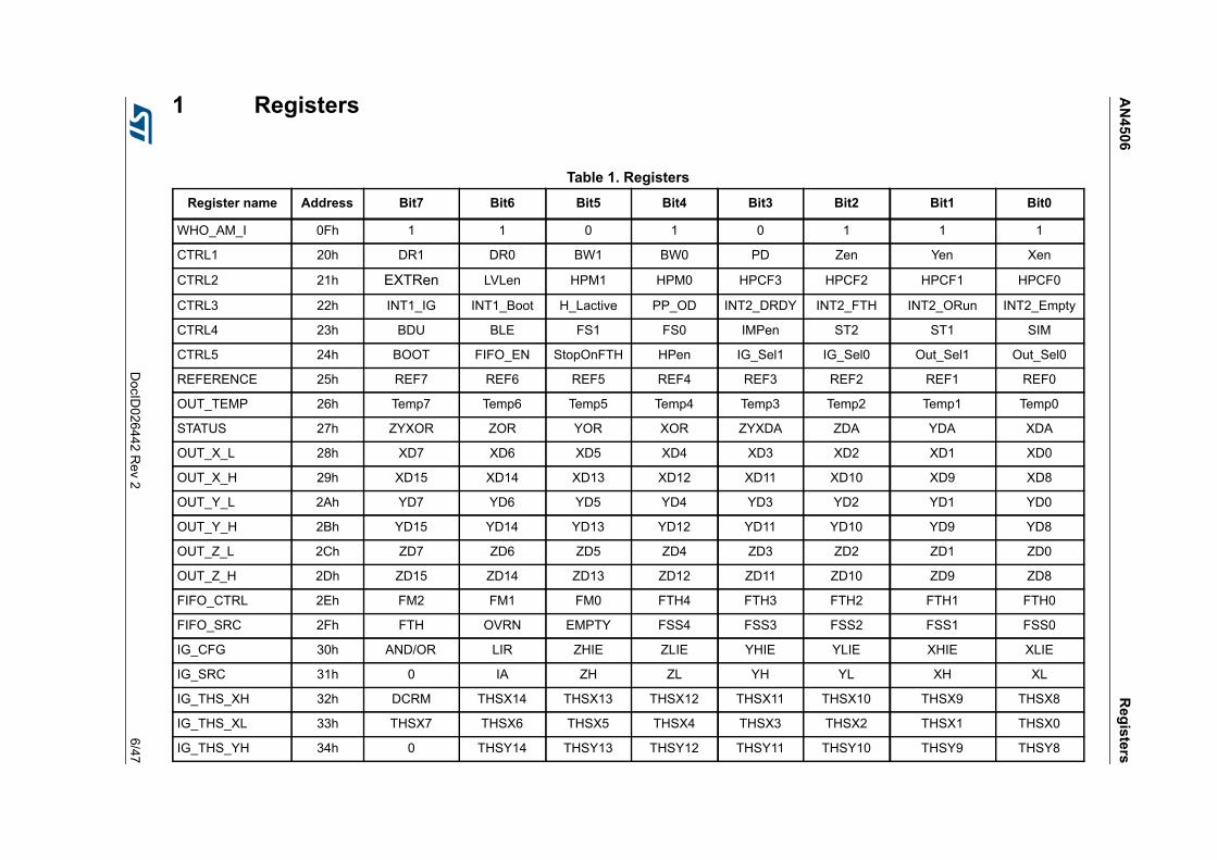
1 Registers
Table 1. RegistersRegister name Address Bit7 Bit6 Bit5 Bit4 Bit3 Bit2 Bit1 Bit0
WHO_AM_I 0Fh 1 1 0 1 0 1 1 1
CTRL1 20h DR1 DR0 BW1 BW0 PD Zen Yen Xen
CTRL2 21h EXTRen LVLen HPM1 HPM0 HPCF3 HPCF2 HPCF1 HPCF0
CTRL3 22h INT1_IG INT1_Boot H_Lactive PP_OD INT2_DRDY INT2_FTH INT2_ORun INT2_Empty
CTRL4 23h BDU BLE FS1 FS0 IMPen ST2 ST1 SIM
CTRL5 24h BOOT FIFO_EN StopOnFTH HPen IG_Sel1 IG_Sel0 Out_Sel1 Out_Sel0
REFERENCE 25h REF7 REF6 REF5 REF4 REF3 REF2 REF1 REF0
OUT_TEMP 26h Temp7 Temp6 Temp5 Temp4 Temp3 Temp2 Temp1 Temp0
STATUS 27h ZYXOR ZOR YOR XOR ZYXDA ZDA YDA XDA
OUT_X_L 28h XD7 XD6 XD5 XD4 XD3 XD2 XD1 XD0
OUT_X_H 29h XD15 XD14 XD13 XD12 XD11 XD10 XD9 XD8
OUT_Y_L 2Ah YD7 YD6 YD5 YD4 YD3 YD2 YD1 YD0
OUT_Y_H 2Bh YD15 YD14 YD13 YD12 YD11 YD10 YD9 YD8
OUT_Z_L 2Ch ZD7 ZD6 ZD5 ZD4 ZD3 ZD2 ZD1 ZD0
OUT_Z_H 2Dh ZD15 ZD14 ZD13 ZD12 ZD11 ZD10 ZD9 ZD8
FIFO_CTRL 2Eh FM2 FM1 FM0 FTH4 FTH3 FTH2 FTH1 FTH0
FIFO_SRC 2Fh FTH OVRN EMPTY FSS4 FSS3 FSS2 FSS1 FSS0
IG_CFG 30h AND/OR LIR ZHIE ZLIE YHIE YLIE XHIE XLIE
IG_SRC 31h 0 IA ZH ZL YH YL XH XL
IG_THS_XH 32h DCRM THSX14 THSX13 THSX12 THSX11 THSX10 THSX9 THSX8
IG_THS_XL 33h THSX7 THSX6 THSX5 THSX4 THSX3 THSX2 THSX1 THSX0
IG_THS_YH 34h 0 THSY14 THSY13 THSY12 THSY11 THSY10 THSY9 THSY8
AN
4506R
egisters
DocID
026442 Rev 2
7/47
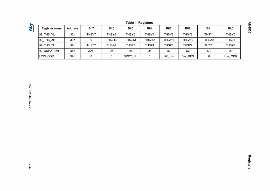
IG_THS_YL 35h THSY7 THSY6 THSY5 THSY4 THSY3 THSY2 THSY1 THSY0
IG_THS_ZH 36h 0 THSZ14 THSZ13 THSZ12 THSZ11 THSZ10 THSZ9 THSZ8
IG_THS_ZL 37h THSZ7 THSZ6 THSZ5 THSZ4 THSZ3 THSZ2 THSZ1 THSZ0
IG_DURATION 38h WAIT D6 D5 D4 D3 D2 D1 D0
LOW_ODR 39h 0 0 DRDY_HL 0 I2C_dis SW_RES 0 Low_ODR
Table 1. RegistersRegister name Address Bit7 Bit6 Bit5 Bit4 Bit3 Bit2 Bit1 Bit0
Operating modes AN4506
8/47 DocID026442 Rev 2
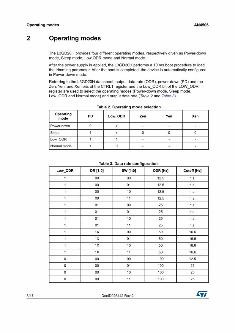
2 Operating modes
The L3GD20H provides four different operating modes, respectively given as Power-down mode, Sleep mode, Low ODR mode and Normal mode.
After the power supply is applied, the L3GD20H performs a 10 ms boot procedure to load the trimming parameter. After the boot is completed, the device is automatically configured in Power-down mode.
Referring to the L3GD20H datasheet, output data rate (ODR), power-down (PD) and the Zen, Yen, and Xen bits of the CTRL1 register and the Low_ODR bit of the LOW_ODR register are used to select the operating modes (Power-down mode, Sleep mode, Low_ODR and Normal mode) and output data rate (Table 2 and Table 3).
Table 2. Operating mode selectionOperating
mode PD Low_ODR Zen Yen Xen
Power down 0 x - - -
Sleep 1 x 0 0 0
Low_ODR 1 1 - - -
Normal mode 1 0 - - -
Table 3. Data rate configuration Low_ODR DR [1:0] BW [1:0] ODR [Hz] Cutoff [Hz]
1 00 00 12.5 n.a.
1 00 01 12.5 n.a.
1 00 10 12.5 n.a.
1 00 11 12.5 n.a.
1 01 00 25 n.a.
1 01 01 25 n.a.
1 01 10 25 n.a.
1 01 11 25 n.a.
1 1X 00 50 16.6
1 1X 01 50 16.6
1 1X 10 50 16.6
1 1X 11 50 16.6
0 00 00 100 12.5
0 00 01 100 25
0 00 10 100 25
0 00 11 100 25
AN4506 Operating modes
DocID026442 Rev 2 9/47
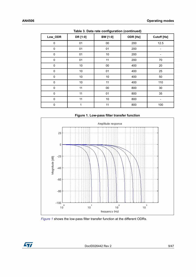
Figure 1. Low-pass filter transfer function
Figure 1 shows the low-pass filter transfer function at the different ODRs.
0 01 00 200 12.5
0 01 01 200 -
0 01 10 200 -
0 01 11 200 70
0 10 00 400 20
0 10 01 400 25
0 10 10 400 50
0 10 11 400 110
0 11 00 800 30
0 11 01 800 35
0 11 10 800 -
0 1 11 800 100
Table 3. Data rate configuration (continued)Low_ODR DR [1:0] BW [1:0] ODR [Hz] Cutoff [Hz]
Operating modes AN4506
10/47 DocID026442 Rev 2
Table 4 shows the typical values of power consumption for the different operating modes. Power consumption in Normal mode is independent of the selected ODR.
2.1 Power-down modeWhen the device is in Power-down mode, almost all internal blocks of the device are switched off to minimize power consumption. Digital interfaces (I2C and SPI) are still active to allow communication with the device. The content of the configuration registers is preserved and output data registers are not updated, therefore keeping the last data sampled in memory before going into Power-down mode.
2.2 Sleep modeWhile the device is in Sleep mode the driving circuitry making the moving mass of the gyroscope oscillating is kept active. Turn-on time from Sleep mode to Normal mode is drastically reduced.
2.3 Low ODR modeIn this mode low speed ODRs are enabled. After setting the Low_ODR bit to ‘1’ in the LOW_ODR register (39h), three low-speed ODRs can be chosen through the DR1 and DR0 bits in the CTRL1 register: 12.5 Hz, 25 Hz and 50 Hz.
Refer to Table 3 for ODR and bandwidth configurations.
Data interrupt generation is active and configured through the IG_CFG register.
2.4 Normal modeIn Normal mode, data are generated at the data rate (ODR) selected through the DR bits. Data interrupt generation is active and configured through the IG_CFG register.
Table 4. Power consumptionOperating mode Power consumption (Vdd = 3 V)
Power-down 0.5 μA
Sleep 2.4 mA
Normal 4.8 mA
AN4506 Reading angular rate data
DocID026442 Rev 2 11/47
2.5 Switching modesThe delay in order to switch modes is shown in Table 5.
3 Reading angular rate data
3.1 Startup sequenceOnce the device is powered up, it automatically downloads the calibration coefficients from the embedded flash to the internal registers. When the boot procedure is completed, i.e. after approximately 10 milliseconds, the device automatically enters Power-down mode. To turn on the device and gather angular rate data, it is necessary to select Normal (or Low ODR) mode and to enable at least one of the axes.
The following general-purpose sequence can be used to configure the device:
Table 5. Turn-on timeStarting mode Target mode Turn-on time - typ.
Power-down Normal 100 ms
Power-down Sleep 100 ms
Power-down Self test 100 ms
Sleep Normal1/ODR: LPF2 disabled6/ODR: LPF2 enabled
Sleep Power-down Immediate
Normal Sleep Immediate
Normal Power-down Immediate
Other settings change -1/ODR: LPF2 disabled6/ODR: LPF2 enabled
1. Write CTRL2
2. Write CTRL3
3. Write CTRL4
4. Write CTRL6
5. Write Reference
6. Write IG_THS
7. Write IG_DURATION
8. Write IG_CFG
9. Write CTRL5
10. Write CTRL1
Reading angular rate data AN4506
12/47 DocID026442 Rev 2
3.2 Using the status registerThe device is provided with a STATUS register which should be polled to check when a new set of data is available. The reading procedure should be the following:
The check performed at step 3 allows the user to understand whether the reading rate is adequate compared to the data production rate. If one or more angular rate samples have been overwritten by new data, because of an insufficient reading rate, the ZYXOR bit of the STATUS register is set to 1.
The overrun bits and the new data available bits are automatically cleared when all the data present inside the device have been read and new data have not been produced in the meantime.
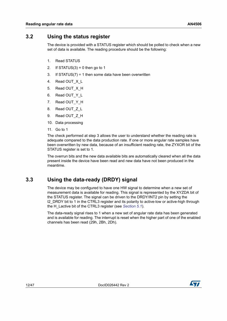
3.3 Using the data-ready (DRDY) signalThe device may be configured to have one HW signal to determine when a new set of measurement data is available for reading. This signal is represented by the XYZDA bit of the STATUS register. The signal can be driven to the DRDY/INT2 pin by setting the I2_DRDY bit to 1 in the CTRL3 register and its polarity to active-low or active-high through the H_Lactive bit of the CTRL3 register (see Section 5.1).
The data-ready signal rises to 1 when a new set of angular rate data has been generated and is available for reading. The interrupt is reset when the higher part of one of the enabled channels has been read (29h, 2Bh, 2Dh).
1. Read STATUS
2. If STATUS(3) = 0 then go to 1
3. If STATUS(7) = 1 then some data have been overwritten
4. Read OUT_X_L
5. Read OUT_X_H
6. Read OUT_Y_L
7. Read OUT_Y_H
8. Read OUT_Z_L
9. Read OUT_Z_H
10. Data processing
11. Go to 1
AN4506 Reading angular rate data
DocID026442 Rev 2 13/47
Figure 2. Data-ready signal
3.4 Using the block data update (BDU) featureIf the reading of the angular rate data is particularly slow and cannot be synchronized (or it is not required) with either the XYZDA bit in the STATUS register or with the DRDY signal, it is strongly recommended to set the BDU (block data update) bit to 1 in the CTRL4 register.
This feature avoids reading values (most significant and least significant parts of the angular rate data) related to different samples. In particular, when the BDU is activated, the data registers related to each channel always contain the most recent angular rate data produced by the device, but, if the reading of a given pair (i.e. OUT_X_H and OUT_X_L, OUT_Y_H and OUT_Y_L, OUT_Z_H and OUT_Z_L) is initiated, the refresh for that pair is blocked until both MSB and LSB parts of the data are read.
Note: BDU only guarantees that OUT_X(Y, Z)_L and OUT_X(Y,Z)_H have been sampled at the same moment. For example, if the reading speed is too slow, it may read X and Y sampled at T1 and Z sampled at T2. Data must be read starting from the lower address.
3.5 DEN functionThe L3GD20H allows external trigger level recognition through enabling the EXTRen (bit7) and LVLen (bit6) bits in CTRL2 (21h) and the IMPen (bit3) bit of CTRL4. Three different modes can be used: level-sensitive, pulse-sensitive and edge-sensitive trigger.
3.5.1 Level-sensitive trigger stamping (LVLen = 1; EXTRen = 0; IMPen = 0)Once enabled, the DEN logical value replaces the less significant bit of X, Y and Z data for the axis selected through the Xen, Yen, and Zen bits in CTRL_REG1 (20h).
Data are stored inside the FIFO with the internally selected ODR.
Table 6. DEN configurationsEXTRen LVLen IMPen Function
1 0 0 Level sensitive
1 0 1 Pulse sensitive
0 1 0 Edge sensitive
Reading angular rate data AN4506
14/47 DocID026442 Rev 2
Figure 3. Data synchronization: level sensitive
Figure 4. Level-sensitive trigger stamping
3.5.2 Pulse sensitive trigger (LVLen = 1; EXTRen = 0; IMPen = 1)The pulse-sensitive trigger is similar to the level-sensitive trigger, and has to be used if the duration of the DEN pulse is shorter than the selected gyroscope ODR. Once enabled, the LSB bit of the gyroscope X, Y, Z output data generated after the pulse is set to 1; if no pulse occurs, the LSB bit of the next generated gyroscope X, Y, Z output data is set to 0.
When ODR selected is 800 Hz, the maximum DEN sample frequency is fDEN = 1/TDEN = 400 Hz.
Figure 5. Data synchronization: pulse sensitive
AN4506 Reading angular rate data
DocID026442 Rev 2 15/47
3.5.3 Edge-sensitive trigger (LVLen = 0; EXTRen = 1; IMPen = 0)Once enabled, the gyroscope output registers are updated with the next generated X, Y, Z gyroscope data at the rising edge of the DEN input signal. If no rising edge occurs, the gyroscope output registers are not updated.
When the ODR selected is 800 Hz, the maximum DEN sample frequency is fDEN = 1/TDEN = 400 Hz.
Figure 6. Data synchronization: edge sensitive
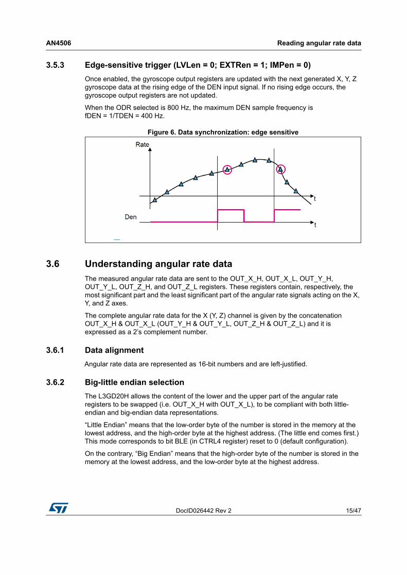
3.6 Understanding angular rate dataThe measured angular rate data are sent to the OUT_X_H, OUT_X_L, OUT_Y_H, OUT_Y_L, OUT_Z_H, and OUT_Z_L registers. These registers contain, respectively, the most significant part and the least significant part of the angular rate signals acting on the X, Y, and Z axes.
The complete angular rate data for the X (Y, Z) channel is given by the concatenation OUT_X_H & OUT_X_L (OUT_Y_H & OUT_Y_L, OUT_Z_H & OUT_Z_L) and it is expressed as a 2’s complement number.
3.6.1 Data alignmentAngular rate data are represented as 16-bit numbers and are left-justified.
3.6.2 Big-little endian selectionThe L3GD20H allows the content of the lower and the upper part of the angular rate registers to be swapped (i.e. OUT_X_H with OUT_X_L), to be compliant with both little-endian and big-endian data representations.
“Little Endian” means that the low-order byte of the number is stored in the memory at the lowest address, and the high-order byte at the highest address. (The little end comes first.) This mode corresponds to bit BLE (in CTRL4 register) reset to 0 (default configuration).
On the contrary, “Big Endian” means that the high-order byte of the number is stored in the memory at the lowest address, and the low-order byte at the highest address.
Digital filters AN4506
16/47 DocID026442 Rev 2
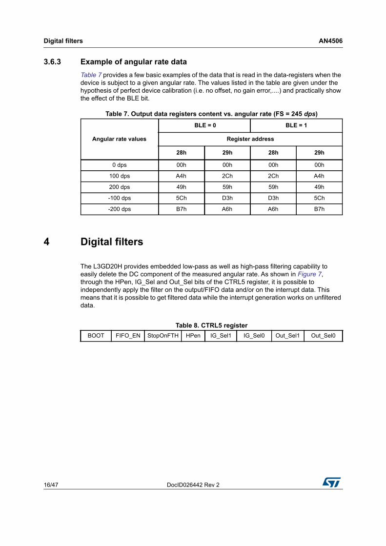
3.6.3 Example of angular rate dataTable 7 provides a few basic examples of the data that is read in the data-registers when the device is subject to a given angular rate. The values listed in the table are given under the hypothesis of perfect device calibration (i.e. no offset, no gain error,....) and practically show the effect of the BLE bit.
4 Digital filters
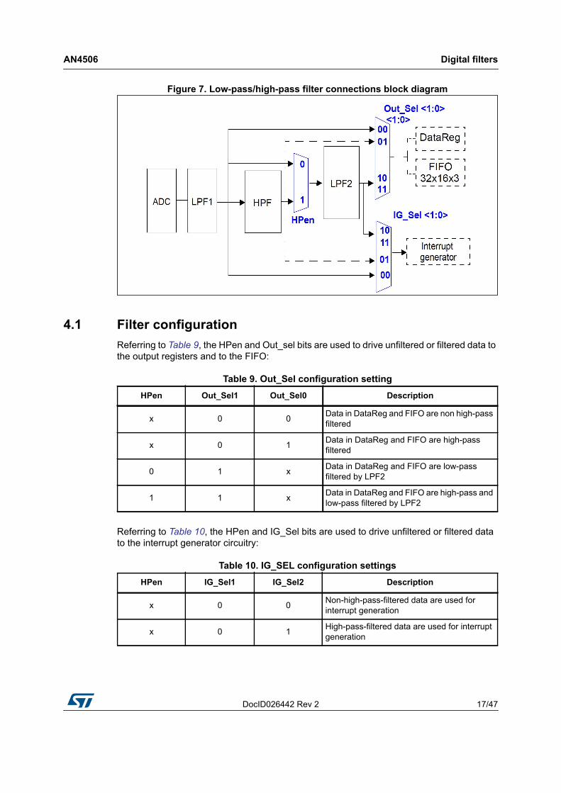
The L3GD20H provides embedded low-pass as well as high-pass filtering capability to easily delete the DC component of the measured angular rate. As shown in Figure 7, through the HPen, IG_Sel and Out_Sel bits of the CTRL5 register, it is possible to independently apply the filter on the output/FIFO data and/or on the interrupt data. This means that it is possible to get filtered data while the interrupt generation works on unfiltered data.
Table 7. Output data registers content vs. angular rate (FS = 245 dps)
Angular rate values
BLE = 0 BLE = 1
Register address
28h 29h 28h 29h
0 dps 00h 00h 00h 00h
100 dps A4h 2Ch 2Ch A4h
200 dps 49h 59h 59h 49h
-100 dps 5Ch D3h D3h 5Ch
-200 dps B7h A6h A6h B7h
Table 8. CTRL5 registerBOOT FIFO_EN StopOnFTH HPen IG_Sel1 IG_Sel0 Out_Sel1 Out_Sel0
AN4506 Digital filters
DocID026442 Rev 2 17/47
Figure 7. Low-pass/high-pass filter connections block diagram
4.1 Filter configurationReferring to Table 9, the HPen and Out_sel bits are used to drive unfiltered or filtered data to the output registers and to the FIFO:
Referring to Table 10, the HPen and IG_Sel bits are used to drive unfiltered or filtered data to the interrupt generator circuitry:
Table 9. Out_Sel configuration settingHPen Out_Sel1 Out_Sel0 Description
x 0 0 Data in DataReg and FIFO are non high-pass filtered
x 0 1 Data in DataReg and FIFO are high-pass filtered
0 1 x Data in DataReg and FIFO are low-pass filtered by LPF2
1 1 x Data in DataReg and FIFO are high-pass and low-pass filtered by LPF2
Table 10. IG_SEL configuration settingsHPen IG_Sel1 IG_Sel2 Description
x 0 0 Non-high-pass-filtered data are used for interrupt generation
x 0 1 High-pass-filtered data are used for interrupt generation
Digital filters AN4506
18/47 DocID026442 Rev 2
4.2 Low-pass filtersThe bandwidth of the low-pass filters depends on the selected ODR. The cutoff frequencies (ft) for the low-pass filters are shown in Table 13.
0 1 x Low-pass-filtered data are used for interrupt generation
1 1 x High-pass and low-pass-filtered data are used for interrupt generation
Table 10. IG_SEL configuration settingsHPen IG_Sel1 IG_Sel2 Description
Table 11. Low-pass filter cutoff frequency
Low_ODR DR [1:0] BW [1:0] ODR [Hz] Cutoff LPF1 [Hz]
Cutoff LPF2 [Hz]
1 00 00 12.5
3.9
n.a.
1 00 01 12.5 n.a.
1 00 10 12.5 n.a.
1 00 11 12.5 n.a.
1 01 00 25
7.8
n.a.
1 01 01 25 n.a.
1 01 10 25 n.a.
1 01 11 25 n.a.
1 1x 00 50
16
16.6
1 1x 01 50 16.6
1 1x 10 50 16.6
1 1x 11 50 16.6
0 00 00 100
32
12.5
0 00 01 100 25
0 00 10 100 25
0 00 11 100 25
0 01 00 200
63.3
12.5
0 01 01 200 -
0 01 10 200 -
0 01 11 200 70
0 10 00 400
128
20
0 10 01 400 25
0 10 10 400 50
0 10 11 400 110
AN4506 Digital filters
DocID026442 Rev 2 19/47
4.3 High-pass filterThe bandwidth of the high-pass filter depends on the selected ODR and on the settings of the HPCFx bits of the CTRL2 register. The high-pass filter cut-off frequencies (ft) are shown in Table 13.
Referring to Table 14, three operating modes are possible for the high-pass filter:
0 11 00 800
211
30
0 11 01 800 35
0 11 10 800 -
0 11 11 800 110
Table 11. Low-pass filter cutoff frequency
Low_ODR DR [1:0] BW [1:0] ODR [Hz] Cutoff LPF1 [Hz]
Cutoff LPF2 [Hz]
Table 12. CTRL2 registerEXTRen LVLen HPM1 HPM0 HPCF3 HPCF2 HPCF1 HPCF0
Table 13. High-pass filter cut-off frequencies [Hz]
HPCF3-0ODR [Hz]
12.5 25 50 100 200 400 800
0000 1 2 4 8 15 30 56
0001 0.5 1 2 4 8 15 30
0010 0.2 0.5 1 2 4 8 15
0011 0.1 0.2 0.5 1 2 4 8
0100 0.05 0.1 0.2 0.5 1 2 4
0101 0.02 0.05 0.1 0.2 0.5 1 2
0110 0.01 0.02 0.05 0.1 0.2 0.5 1
0111 0.005 0.01 0.02 0.05 0.1 0.2 0.5
1000 0.002 0.005 0.01 0.02 0.05 0.1 0.2
1001 0.001 0.002 0.005 0.01 0.02 0.05 0.1
Table 14. High-pass filter mode configurationHPM1 HPM0 High-pass filter mode
0 0 Normal mode (reset by reading the REFERENCE register)
0 1 Reference signal for filtering
Digital filters AN4506
20/47 DocID026442 Rev 2
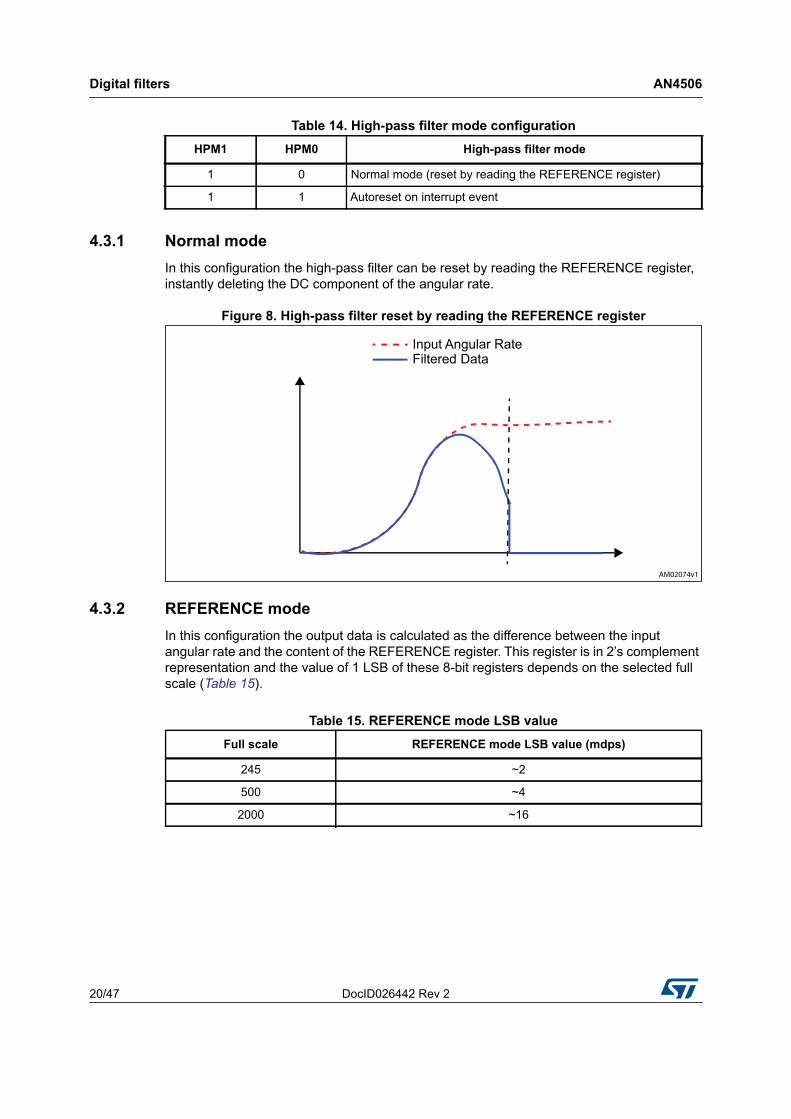
4.3.1 Normal modeIn this configuration the high-pass filter can be reset by reading the REFERENCE register, instantly deleting the DC component of the angular rate.
Figure 8. High-pass filter reset by reading the REFERENCE register
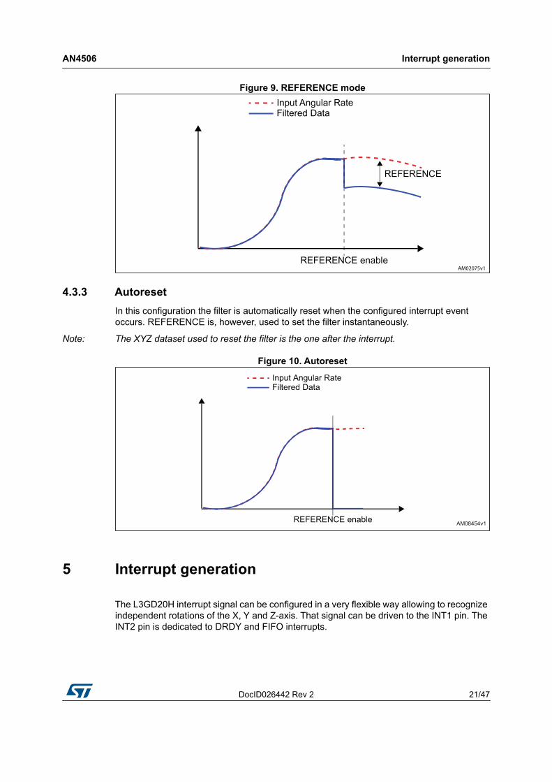
4.3.2 REFERENCE modeIn this configuration the output data is calculated as the difference between the input angular rate and the content of the REFERENCE register. This register is in 2’s complement representation and the value of 1 LSB of these 8-bit registers depends on the selected full scale (Table 15).
1 0 Normal mode (reset by reading the REFERENCE register)
1 1 Autoreset on interrupt event
Table 14. High-pass filter mode configurationHPM1 HPM0 High-pass filter mode
Table 15. REFERENCE mode LSB valueFull scale REFERENCE mode LSB value (mdps)
245 ~2
500 ~4
2000 ~16
AN4506 Interrupt generation
DocID026442 Rev 2 21/47
Figure 9. REFERENCE mode
4.3.3 AutoresetIn this configuration the filter is automatically reset when the configured interrupt event occurs. REFERENCE is, however, used to set the filter instantaneously.
Note: The XYZ dataset used to reset the filter is the one after the interrupt.
Figure 10. Autoreset
5 Interrupt generation
The L3GD20H interrupt signal can be configured in a very flexible way allowing to recognize independent rotations of the X, Y and Z-axis. That signal can be driven to the INT1 pin. The INT2 pin is dedicated to DRDY and FIFO interrupts.
Interrupt generation AN4506
22/47 DocID026442 Rev 2
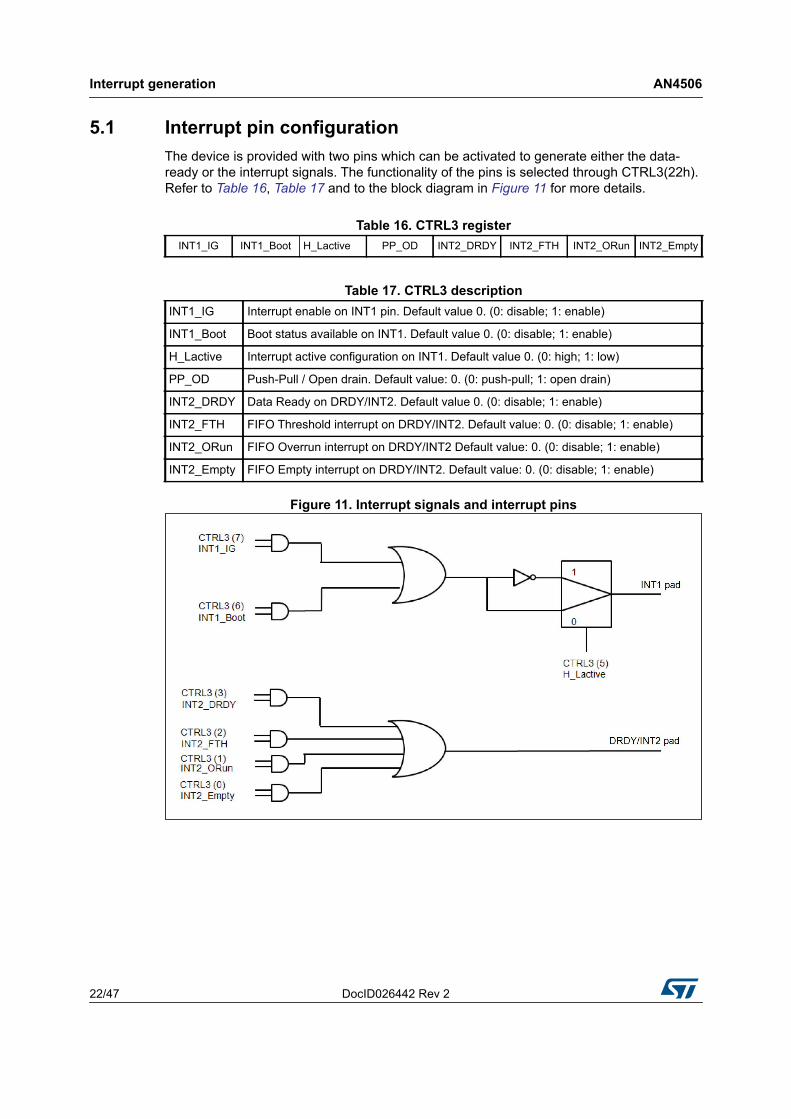
5.1 Interrupt pin configurationThe device is provided with two pins which can be activated to generate either the data-ready or the interrupt signals. The functionality of the pins is selected through CTRL3(22h). Refer to Table 16, Table 17 and to the block diagram in Figure 11 for more details.
Figure 11. Interrupt signals and interrupt pins
Table 16. CTRL3 registerINT1_IG INT1_Boot H_Lactive PP_OD INT2_DRDY INT2_FTH INT2_ORun INT2_Empty
Table 17. CTRL3 descriptionINT1_IG Interrupt enable on INT1 pin. Default value 0. (0: disable; 1: enable)
INT1_Boot Boot status available on INT1. Default value 0. (0: disable; 1: enable)
H_Lactive Interrupt active configuration on INT1. Default value 0. (0: high; 1: low)
PP_OD Push-Pull / Open drain. Default value: 0. (0: push-pull; 1: open drain)
INT2_DRDY Data Ready on DRDY/INT2. Default value 0. (0: disable; 1: enable)
INT2_FTH FIFO Threshold interrupt on DRDY/INT2. Default value: 0. (0: disable; 1: enable)
INT2_ORun FIFO Overrun interrupt on DRDY/INT2 Default value: 0. (0: disable; 1: enable)
INT2_Empty FIFO Empty interrupt on DRDY/INT2. Default value: 0. (0: disable; 1: enable)
AN4506 Interrupt generation
DocID026442 Rev 2 23/47
5.2 Interrupt configurationThe L3GD20H offers several possibilities to personalize the interrupt signal. The registers involved in the interrupt generation behavior are IG_CFG, IG_THS and IG_DURATION.
Whenever an interrupt condition is verified the interrupt signal is generated and by reading the IG_SRC register it is possible to understand which condition happened.
Reading IG_SRC also clears the IG_SRC IA bit (and eventually the interrupt signal on the INT1 pin) and allows the refresh of data in the IG_SRC register if the latched option was chosen.
Table 18. IG_CFG registerAND/OR LIR ZHIE ZLIE YHIE YLIE XHIE XLIE
Table 19. IG_CFG description
AND/ORAND/OR combination of interrupt events. Default value: 0(0: OR combination of interrupt events 1: AND combination of interrupt events
LIRLatch interrupt request. Default value: 0(0: interrupt request not latched; 1: interrupt request latched)Cleared by reading IG_SRC reg.
ZHIEEnable interrupt generation on Z high event. Default value: 0(0: disable interrupt request; 1: enable interrupt request on measured rate value higher than preset threshold)
ZLIEEnable interrupt generation on Z low event. Default value: 0(0: disable interrupt request; 1: enable interrupt request on measured rate value lower than preset threshold)
YHIEEnable interrupt generation on Y high event. Default value: 0(0: disable interrupt request; 1: enable interrupt request on measured rate value higher than preset threshold)
YLIEEnable interrupt generation on Y low event. Default value: 0(0: disable interrupt request; 1: enable interrupt request on measured rate value lower than preset threshold)
XHIEEnable interrupt generation on X high event. Default value: 0 (0: disable interrupt request; 1: enable interrupt request on measured rate value higher than preset threshold)
XLIEEnable interrupt generation on X low event. Default value: 0 (0: disable interrupt request; 1: enable interrupt request on measured rate value lower than preset threshold)
Table 20. Interrupt mode configurationAND/OR Interrupt mode
0 OR combination of interrupt events
1 AND combination of interrupt events
Interrupt generation AN4506
24/47 DocID026442 Rev 2
5.3 ThresholdThreshold registers IG_THS_xH and IG_THS_xL (respectively MSB and LSB) define the reference angular rates used by interrupt generation circuitry.
The value of 1 LSB of the threshold depends on the selected full scale (Table 23).
5.4 DurationThe content of the Dx bits in the IG_DURATION register sets the minimum duration of the interrupt event to be recognized.
Duration steps and maximum values depend on the ODR chosen.
Duration time is measured in N/ODR, where N is the content of the duration register and ODR is 12.5, 25, 50, 100, 200, 400, and 800.
Table 21. IG_THS_xH register- THSx14 THSx13 THSx12 THSx11 THSx10 THSx9 THSx8
Table 22. IG_THS_xL registerTHSx7 THSx6 THSx5 THSx4 THSx3 THSx2 THSx1 THSx0
Table 23. Threshold LSB valueFull scale (dps) Threshold LSB value (mdps)
245 ~7.5
500 ~15.3
2000 ~61
Table 24. IG_DURATION registerWAIT D6 D5 D4 D3 D2 D1 D0
Table 25. IG_DURATION descriptionWAIT WAIT enable. Default value: 0 (0: disable; 1: enable)
D6 - D0 Duration value. Default value: 000 0000
Table 26. Duration LSB value in Normal modeODR (Hz) Duration LSB value (ms)
12.5 80
25 40
50 20
100 10
AN4506 Interrupt generation
DocID026442 Rev 2 25/47
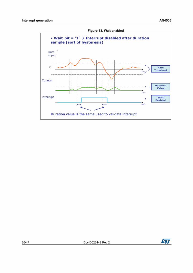
The WAIT bit of the IG_DURATION register has the following meaning:
Wait = ‘0’: the interrupt falls immediately if signal crosses the selected threshold (Figure 12).
Wait = ‘1’: if signal crosses the selected threshold, the interrupt falls only after the duration has counted the number of samples at the selected data rate, written into the duration counter register (Figure 13).
Figure 12. Wait disabled
200 5
400 2.5
800 1.25
Table 26. Duration LSB value in Normal modeODR (Hz) Duration LSB value (ms)
• Wait bit = ‘0’ �� Interrupt disabled as soon as condition is no longer valid (ex: Rate value below threshold)
Rate(dps)
Rate Threshold
0t(n)
t(n)
t(n)
Interrupt
Counter
Duration Value
“Wait” Disabled
Interrupt generation AN4506
26/47 DocID026442 Rev 2
Figure 13. Wait enabled
• Wait bit = ‘1’ �� Interrupt disabled after duration sample (sort of hysteresis)
Rate(dps)
Rate Threshold
0t(n)
t(n)
t(n)
Interrupt
Counter
Duration Value
“Wait” Enabled
Duration value is the same used to validate interrupt
AN4506 Interrupt generation
DocID026442 Rev 2 27/47
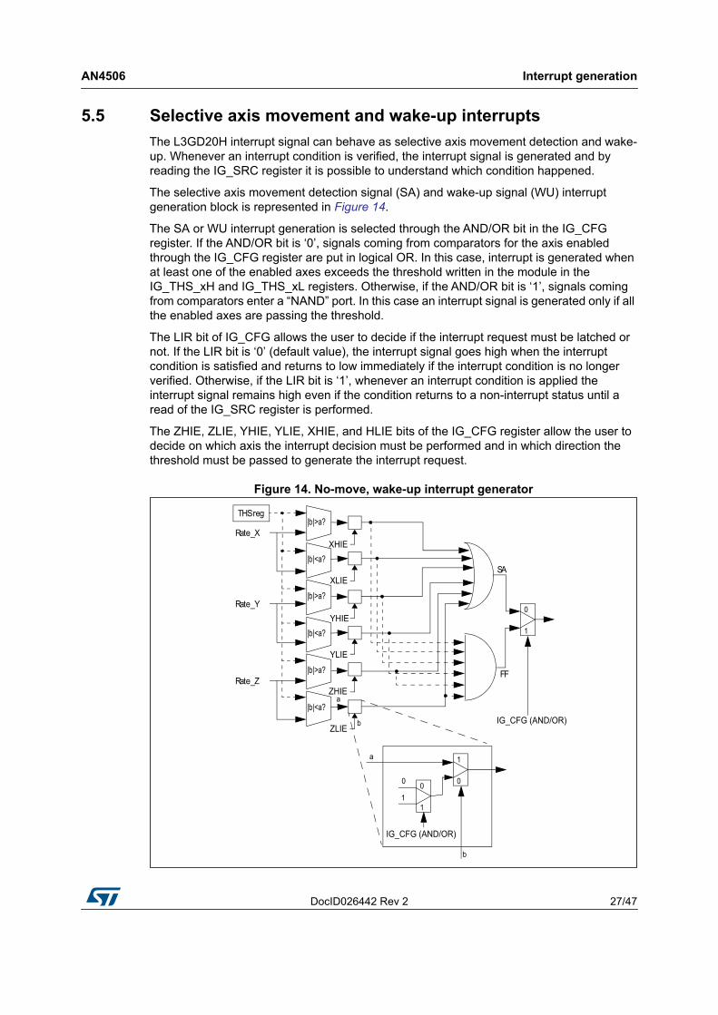
5.5 Selective axis movement and wake-up interruptsThe L3GD20H interrupt signal can behave as selective axis movement detection and wake-up. Whenever an interrupt condition is verified, the interrupt signal is generated and by reading the IG_SRC register it is possible to understand which condition happened.
The selective axis movement detection signal (SA) and wake-up signal (WU) interrupt generation block is represented in Figure 14.
The SA or WU interrupt generation is selected through the AND/OR bit in the IG_CFG register. If the AND/OR bit is ‘0’, signals coming from comparators for the axis enabled through the IG_CFG register are put in logical OR. In this case, interrupt is generated when at least one of the enabled axes exceeds the threshold written in the module in the IG_THS_xH and IG_THS_xL registers. Otherwise, if the AND/OR bit is ‘1’, signals coming from comparators enter a “NAND” port. In this case an interrupt signal is generated only if all the enabled axes are passing the threshold.
The LIR bit of IG_CFG allows the user to decide if the interrupt request must be latched or not. If the LIR bit is ‘0’ (default value), the interrupt signal goes high when the interrupt condition is satisfied and returns to low immediately if the interrupt condition is no longer verified. Otherwise, if the LIR bit is ‘1’, whenever an interrupt condition is applied the interrupt signal remains high even if the condition returns to a non-interrupt status until a read of the IG_SRC register is performed.
The ZHIE, ZLIE, YHIE, YLIE, XHIE, and HLIE bits of the IG_CFG register allow the user to decide on which axis the interrupt decision must be performed and in which direction the threshold must be passed to generate the interrupt request.
Figure 14. No-move, wake-up interrupt generator
Interrupt generation AN4506
28/47 DocID026442 Rev 2
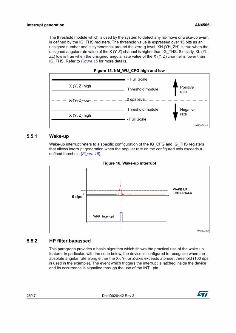
The threshold module which is used by the system to detect any no-move or wake-up event is defined by the IG_THS registers. The threshold value is expressed over 15 bits as an unsigned number and is symmetrical around the zero-g level. XH (YH, ZH) is true when the unsigned angular rate value of the X (Y, Z) channel is higher than IG_THS. Similarly, XL (YL, ZL) low is true when the unsigned angular rate value of the X (Y, Z) channel is lower than IG_THS. Refer to Figure 15 for more details.
Figure 15. NM_WU_CFG high and low
5.5.1 Wake-upWake-up interrupt refers to a specific configuration of the IG_CFG and IG_THS registers that allows interrupt generation when the angular rate on the configured axis exceeds a defined threshold (Figure 16).
Figure 16. Wake-up interrupt
5.5.2 HP filter bypassedThis paragraph provides a basic algorithm which shows the practical use of the wake-up feature. In particular, with the code below, the device is configured to recognize when the absolute angular rate along either the X-, Y-, or Z-axis exceeds a preset threshold (100 dps is used in the example). The event which triggers the interrupt is latched inside the device and its occurrence is signalled through the use of the INT1 pin.
0 dps
AN4506 Interrupt generation
DocID026442 Rev 2 29/47
5.5.3 Using the HP filterThe code provided below gives a basic routine which shows the practical use of the wake-up feature performed on high-pass filtered data. In particular, the device is configured to recognize when the high-frequency component of the angular rate applied along either the X, Y, or Z-axis exceeds a preset threshold (100 dps is used in the example). The event which triggers the interrupt is latched inside the device and its occurrence is signaled through the use of the INT1 pin.
1 Write 0Fh into CTRL1// Turn on the sensor and enable X, Y, and Z// ODR = 100 Hz
2 Write 00h into CTRL2 // High-pass filter disabled
3 Write 80h into CTRL3 // Interrupt driven to INT1 pad
4 Write 00h into CTRL4 // FS = 245 dps
5 Write 34h into IG_THS_XH // Threshold = 100 dps
6 Write 3Eh into IG_THS_XL // Threshold = 100 dps
7 Write 00h into IG_DURATION // Duration = 0
8 Write 02h into IG_CFG // Enable XH interrupt generation
9 Poll INT1 pad; if INT1=0 then go to 8// Poll INT1 pin waiting for the// wake-up event
10 Read IG_SRC // Return the event that has triggered the// interrupt
11 (Wake-up event has occurred; insert your code here) // Event handling
12 Go to 8
1 Write 0Fh into CTRL1// Turn on the sensor and enable X, Y, and Z// ODR = 100 Hz
2 Write 00h into CTRL2 // High-pass filter in Normal mode
3 Write 80h into CTRL3 // Interrupt driven to INT1 pad
4 Write 00h into CTRL4 // FS = 245 dps
5 Write 05h into CTRL5// Data in DataReg and FIFO are high-pass filtered.// High-pass-filtered data are used for interrupt// generation
6 Write 34h into IG_THS_XH // Threshold = 100 dps
7 Write 3Eh into IG_THS_XL // Threshold = 100 dps
8 Write 34h into IG_THS_YH // Threshold = 100 dps
9 Write 3Eh into IG_THS_YL // Threshold = 100 dps
10 Write 34h into IG_THS_ZH // Threshold = 100 dps
11 Write 3Eh into IG_THS_ZL // Threshold = 100 dps
12 Write 00h into IG_DURATION // Duration = 0
Interrupt generation AN4506
30/47 DocID026442 Rev 2
At step 13, a dummy read of the REFERENCE register is performed to set the current/reference angular rate/tilt state against which the device performed the threshold comparison.
This read may be performed any time it is required to set current rate as a reference state without waiting for the filter to settle.
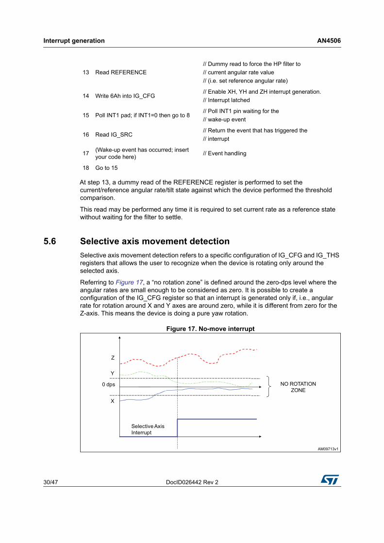
5.6 Selective axis movement detectionSelective axis movement detection refers to a specific configuration of IG_CFG and IG_THS registers that allows the user to recognize when the device is rotating only around the selected axis.
Referring to Figure 17, a “no rotation zone” is defined around the zero-dps level where the angular rates are small enough to be considered as zero. It is possible to create a configuration of the IG_CFG register so that an interrupt is generated only if, i.e., angular rate for rotation around X and Y axes are around zero, while it is different from zero for the Z-axis. This means the device is doing a pure yaw rotation.
Figure 17. No-move interrupt
13 Read REFERENCE // Dummy read to force the HP filter to// current angular rate value// (i.e. set reference angular rate)
14 Write 6Ah into IG_CFG// Enable XH, YH and ZH interrupt generation.// Interrupt latched
15 Poll INT1 pad; if INT1=0 then go to 8// Poll INT1 pin waiting for the// wake-up event
16 Read IG_SRC // Return the event that has triggered the// interrupt
17 (Wake-up event has occurred; insert your code here) // Event handling
18 Go to 15
AN4506 Interrupt generation
DocID026442 Rev 2 31/47
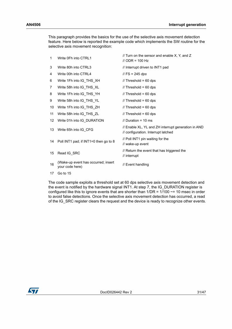
This paragraph provides the basics for the use of the selective axis movement detection feature. Here below is reported the example code which implements the SW routine for the selective axis movement recognition:
The code sample exploits a threshold set at 60 dps selective axis movement detection and the event is notified by the hardware signal INT1. At step 7, the IG_DURATION register is configured like this to ignore events that are shorter than 1/DR = 1/100 ~= 10 msec in order to avoid false detections. Once the selective axis movement detection has occurred, a read of the IG_SRC register clears the request and the device is ready to recognize other events.
1 Write 0Fh into CTRL1// Turn on the sensor and enable X, Y, and Z// ODR = 100 Hz
3 Write 80h into CTRL3 // Interrupt driven to INT1 pad
4 Write 00h into CTRL4 // FS = 245 dps
6 Write 1Fh into IG_THS_XH // Threshold = 60 dps
7 Write 58h into IG_THS_XL // Threshold = 60 dps
8 Write 1Fh into IG_THS_YH // Threshold = 60 dps
9 Write 58h into IG_THS_YL // Threshold = 60 dps
10 Write 1Fh into IG_THS_ZH // Threshold = 60 dps
11 Write 58h into IG_THS_ZL // Threshold = 60 dps
12 Write 01h into IG_DURATION // Duration = 10 ms
13 Write 65h into IG_CFG// Enable XL, YL and ZH interrupt generation in AND // configuration. Interrupt latched
14 Poll INT1 pad; if INT1=0 then go to 8// Poll INT1 pin waiting for the// wake-up event
15 Read IG_SRC // Return the event that has triggered the// interrupt
16 (Wake-up event has occurred; insert your code here) // Event handling
17 Go to 15
First-in first-out (FIFO) buffer AN4506
32/47 DocID026442 Rev 2
6 First-in first-out (FIFO) buffer
In order to limit intervention from the host processor and facilitate post-processing data for event recognition, the L3GD20H embeds a first-in first-out buffer (FIFO) for each of the three output channels, X, Y, and Z.
FIFO use allows consistent power saving for the system; it can wake up only when needed and burst the significant data out from the FIFO.
The FIFO buffer can work according to seven different modes that guarantee a high-level of flexibility during application development: Bypass mode, FIFO mode, Stream mode, Dynamic Stream mode, Stream-to-FIFO mode, Bypass-to-Stream mode and Bypass-to-FIFO mode.
The programmable FIFO threshold and FIFO overrun event can be enabled to generate dedicated interrupts on the DRDY/INT2 pin.
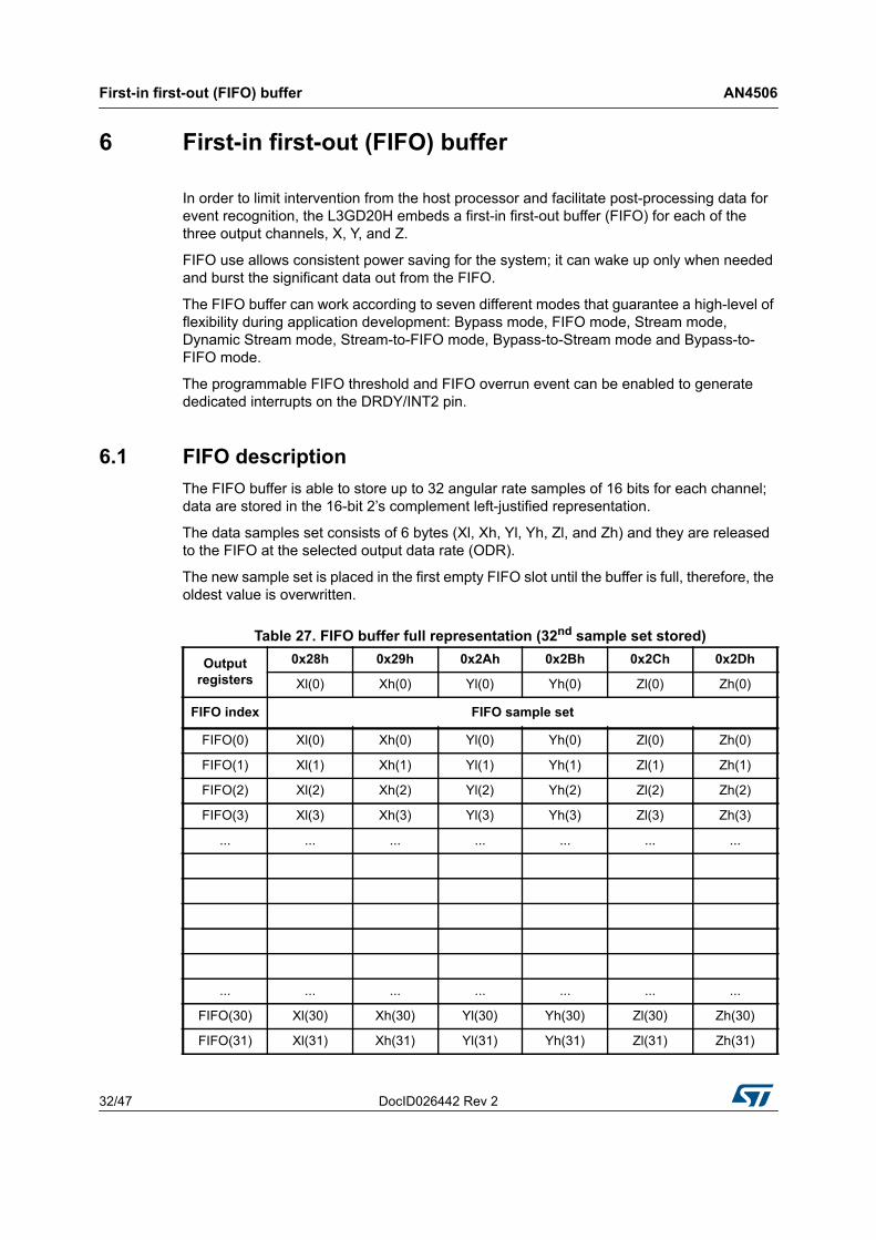
6.1 FIFO descriptionThe FIFO buffer is able to store up to 32 angular rate samples of 16 bits for each channel; data are stored in the 16-bit 2’s complement left-justified representation.
The data samples set consists of 6 bytes (Xl, Xh, Yl, Yh, Zl, and Zh) and they are released to the FIFO at the selected output data rate (ODR).
The new sample set is placed in the first empty FIFO slot until the buffer is full, therefore, the oldest value is overwritten.
Table 27. FIFO buffer full representation (32nd sample set stored)
Output registers
0x28h 0x29h 0x2Ah 0x2Bh 0x2Ch 0x2Dh
Xl(0) Xh(0) Yl(0) Yh(0) Zl(0) Zh(0)
FIFO index FIFO sample set
FIFO(0) Xl(0) Xh(0) Yl(0) Yh(0) Zl(0) Zh(0)
FIFO(1) Xl(1) Xh(1) Yl(1) Yh(1) Zl(1) Zh(1)
FIFO(2) Xl(2) Xh(2) Yl(2) Yh(2) Zl(2) Zh(2)
FIFO(3) Xl(3) Xh(3) Yl(3) Yh(3) Zl(3) Zh(3)
... ... ... ... ... ... ...
... ... ... ... ... ... ...
FIFO(30) Xl(30) Xh(30) Yl(30) Yh(30) Zl(30) Zh(30)
FIFO(31) Xl(31) Xh(31) Yl(31) Yh(31) Zl(31) Zh(31)
AN4506 First-in first-out (FIFO) buffer
DocID026442 Rev 2 33/47
Table 27 represents the FIFO full status when 32 samples are stored in the buffer while Table 28 represents the next step when the 33rd sample is inserted into FIFO and the 1st sample is overwritten. The new oldest sample set is made available in the output registers.
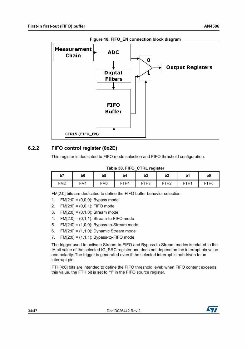
When FIFO is enabled and the mode is different from Bypass, the L3GD20H output registers (28h to 2Dh) always contain the oldest FIFO sample set.
6.2 FIFO registersThe FIFO buffer is managed by three different gyroscope registers, two of these allow enabling and configuring FIFO behavior, the third provides information about the buffer status.
6.2.1 Control register 5 (0x24)The FIFO_EN bit in CTRL5 must be set to 1 in order to enable the internal first-in first-out buffer; while this bit is set, the gyroscope output registers (28h to 2Dh) do not contain the current angular rate value but they always contain the oldest value stored in FIFO.
Table 28. FIFO overrun representation (33rd sample set stored and 1st sample discarded)
Output registers
0x28h 0x29h 0x2Ah 0x2Bh 0x2Ch 0x2Dh
Xl(1) Xh(1) Yl(1) Yh(1) Zl(1) Zh(1)
FIFO index Sample set
FIFO(0) Xl(1) Xh(1) Yl(1) Yh(1) Zl(1) Zh(1)
FIFO(1) Xl(2) Xh(2) Yl(2) Yh(2) Zl(2) Zh(2)
FIFO(2) Xl(3) Xh(3) Yl(3) Yh(3) Zl(3) Zh(3)
FIFO(3) Xl(4) Xh(4) Yl(4) Yh(4) Zl(4) Zh(4)
... ... ... ... ... ... ...
... ... ... ... ... ... ...
FIFO(30) Xl(31) Xh(31) Yl(31) Yh(31) Zl(31) Zh(31)
FIFO(31) Xl(32) Xh(32) Yl(32) Yh(32) Zl(32) Zh(32)
Table 29. FIFO enable bit in CTRL5b7 b6 b5 b4 b3 b2 b1 b0
X FIFO_EN X X X X X X
First-in first-out (FIFO) buffer AN4506
34/47 DocID026442 Rev 2
Figure 18. FIFO_EN connection block diagram
6.2.2 FIFO control register (0x2E)This register is dedicated to FIFO mode selection and FIFO threshold configuration.
FM[2:0] bits are dedicated to define the FIFO buffer behavior selection:1. FM[2:0] = (0,0,0): Bypass mode2. FM[2:0] = (0,0,1): FIFO mode3. FM[2:0] = (0,1,0): Stream mode4. FM[2:0] = (0,1,1): Stream-to-FIFO mode5. FM[2:0] = (1,0,0): Bypass-to-Stream mode6. FM[2:0] = (1,1,0): Dynamic Stream mode7. FM[2:0] = (1,1,1): Bypass-to-FIFO mode
The trigger used to activate Stream-to-FIFO and Bypass-to-Stream modes is related to the IA bit value of the selected IG_SRC register and does not depend on the interrupt pin value and polarity. The trigger is generated even if the selected interrupt is not driven to an interrupt pin.
FTH[4:0] bits are intended to define the FIFO threshold level; when FIFO content exceeds this value, the FTH bit is set to “1” in the FIFO source register.
Table 30. FIFO_CTRL registerb7 b6 b5 b4 b3 b2 b1 b0
FM2 FM1 FM0 FTH4 FTH3 FTH2 FTH1 FTH0
AN4506 First-in first-out (FIFO) buffer
DocID026442 Rev 2 35/47
6.2.3 FIFO source register (0x2F)This register is updated at every ODR and provides information about the FIFO buffer status.
FTH bit is set high when FIFO content exceeds FIFO threshold. OVRN bit is set high when FIFO buffer is full; this means that the FIFO buffer contains
32 unread samples. At the following ODR a new sample set replaces the oldest FIFO value. The OVRN bit is reset when the first sample set has been read.
EMPTY flag is set high when all FIFO samples have been read and FIFO is empty. FSS[4:0] field always contains the current number of unread samples stored in the
FIFO buffer. When FIFO is enabled, this value increases at ODR frequency until the buffer is full, whereas, it decreases every time that one sample set is retrieved from FIFO.
Register content is updated synchronous to the FIFO write and read operation.
The FIFO threshold flag, the FIFO overrun and FIFO empty event can be enabled to generate a dedicated interrupt on the DRDY/INT2 pin by configuring CTRL3.
INT2_FTH bit drives FIFO threshold flag (FTH) on the DRDY/INT2 pin INT2_ORun bit drives Overrun event (OVRN) on the DRDY/INT2Y pin INT2_Empty bit drives Empty event (EMPTY) on the DRDY/INT2 pin.
If one or more bits are set to “1”, the DRDY/INT2 pin status is the logical OR combination of the three signals.
Table 31. FIFO_SRC registerb7 b6 b5 b4 b3 b2 b1 b0
FTH OVRN EMPTY FSS4 FSS3 FSS2 FSS1 FSS0
Table 32. FIFO_SRC_REG behavior assuming FTH[4:0] = 15FTH OVRN EMPTY FSS[4:0] Unread FIFO samples Timing
0 0 1 00000 0 t0
0 0 0 00001 1 t0 + 1/ODR
0 0 0 00010 2 t0 + 2/ODR
... ... ... ... ... ...
0 0 0 01111 15 t0 + 15/ODR
1 0 0 10000 16 t0 + 16/ODR
... ... ... ... ... ...
1 0 0 11110 30 t0 + 30/ODR
1 0 0 11111 31 t0 + 31/ODR
1 1 0 11111 32 t0 + 32/ODR
Table 33. CTRL3 (0x22)b7 b6 b5 b4 b3 b2 b1 b0
X X X X X INT2_FTH INT2_ORun INT2_Empty
First-in first-out (FIFO) buffer AN4506
36/47 DocID026442 Rev 2
6.3 FIFO modesThe L3GD20H FIFO buffer can be configured to operate in five different modes selectable by the FM[2:0] field in the FIFO_CTRL register. Available configurations ensure a high level of flexibility and extend the number of functions usable in application development.
Bypass, FIFO, Stream, Dynamic Stream, Stream-to-FIFO, Bypass-to-Stream and Bypass-to-FIFO modes are described in the following paragraphs.
6.3.1 Bypass modeWhen Bypass mode is enabled, FIFO is not operational: buffer content is cleared, output registers (0x28 to 0x2D) are frozen at the last value loaded, and the FIFO buffer remains empty until another mode is selected.
Follow these steps for Bypass mode configuration:1. Turn on FIFO by setting the FIFO_En bit to “1” in control register 5 (0x24). After this
operation the FIFO buffer is enabled but isn’t collecting data, output registers are frozen to the last sample set loaded.
2. Activate Bypass mode by setting the FM[2:0] field to “000” in the FIFO_CTRL register (0x2E). If this mode is enabled, the FIFO_SRC register (0x2F) is forced equal to 0x20.
Bypass mode must be used in order to stop and reset the FIFO buffer when a different mode is operating. Note that setting the FIFO buffer in Bypass mode clears the whole buffer content.
6.3.2 FIFO modeIn FIFO mode, the buffer continues filling until full (32 sample sets stored,) then it stops collecting data and the FIFO content remains unchanged until a different mode is selected.
Follow these steps for FIFO mode configuration:1. Turn on FIFO by setting the FIFO_En bit to “1” in control register 5 (0x24). After this
operation the FIFO buffer is enabled but is not collecting data, output registers are frozen to the last samples set loaded.
2. Activate FIFO mode by setting the FM[2:0] field to “001” in the FIFO control register (0x2E).
By selecting this mode, FIFO starts data collection and the source register (0x2F) changes according to the number of samples stored. At the end of the procedure, the FIFO source register is set to 0xDF and the OVRN flag generates an interrupt if the INT2_ORun bit is set to 1 in the CTRL3 register. Data can be retrieved when the OVRN is “1”, by performing a 32 sample set read from the output registers. Data can also be retrieved on the FTH flag instead of the OVRN when the application requires a lower number of samples. Communication speed is not so important in FIFO mode because data collection is stopped and there is no risk of overwriting data already acquired. Before restarting FIFO mode, at the end of the reading procedure, it is necessary to set Bypass mode (to clear the FIFO content).
AN4506 First-in first-out (FIFO) buffer
DocID026442 Rev 2 37/47
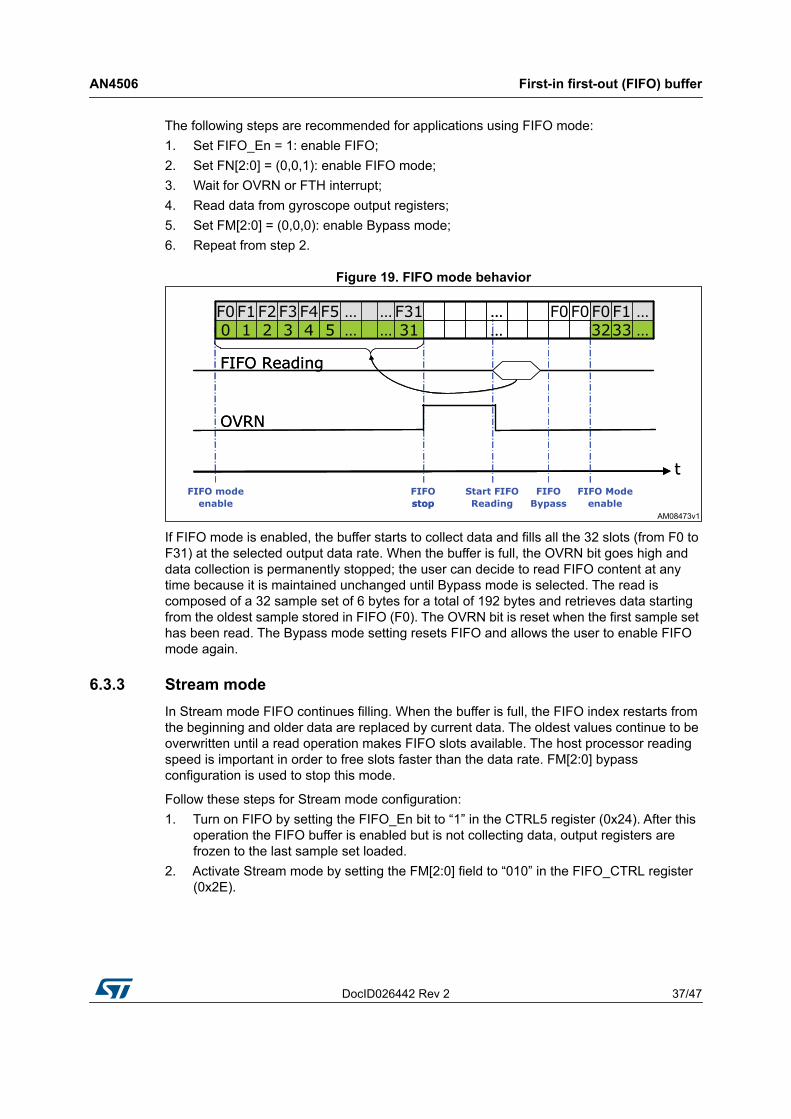
The following steps are recommended for applications using FIFO mode:1. Set FIFO_En = 1: enable FIFO;2. Set FN[2:0] = (0,0,1): enable FIFO mode;3. Wait for OVRN or FTH interrupt;4. Read data from gyroscope output registers;5. Set FM[2:0] = (0,0,0): enable Bypass mode;6. Repeat from step 2.
Figure 19. FIFO mode behavior
If FIFO mode is enabled, the buffer starts to collect data and fills all the 32 slots (from F0 to F31) at the selected output data rate. When the buffer is full, the OVRN bit goes high and data collection is permanently stopped; the user can decide to read FIFO content at any time because it is maintained unchanged until Bypass mode is selected. The read is composed of a 32 sample set of 6 bytes for a total of 192 bytes and retrieves data starting from the oldest sample stored in FIFO (F0). The OVRN bit is reset when the first sample set has been read. The Bypass mode setting resets FIFO and allows the user to enable FIFO mode again.
6.3.3 Stream modeIn Stream mode FIFO continues filling. When the buffer is full, the FIFO index restarts from the beginning and older data are replaced by current data. The oldest values continue to be overwritten until a read operation makes FIFO slots available. The host processor reading speed is important in order to free slots faster than the data rate. FM[2:0] bypass configuration is used to stop this mode.
Follow these steps for Stream mode configuration:1. Turn on FIFO by setting the FIFO_En bit to “1” in the CTRL5 register (0x24). After this
operation the FIFO buffer is enabled but is not collecting data, output registers are frozen to the last sample set loaded.
2. Activate Stream mode by setting the FM[2:0] field to “010” in the FIFO_CTRL register (0x2E).
First-in first-out (FIFO) buffer AN4506
38/47 DocID026442 Rev 2
As described for FIFO mode, data can be retrieved when OVRN is set to “1” performing a 32 sample set reading from the output registers; data can be retrieved also on the FTH flag if the application requires a lower number of samples (see Section 6.3.4).
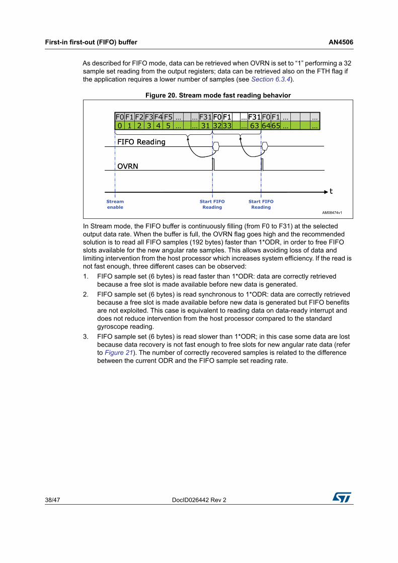
Figure 20. Stream mode fast reading behavior
In Stream mode, the FIFO buffer is continuously filling (from F0 to F31) at the selected output data rate. When the buffer is full, the OVRN flag goes high and the recommended solution is to read all FIFO samples (192 bytes) faster than 1*ODR, in order to free FIFO slots available for the new angular rate samples. This allows avoiding loss of data and limiting intervention from the host processor which increases system efficiency. If the read is not fast enough, three different cases can be observed:1. FIFO sample set (6 bytes) is read faster than 1*ODR: data are correctly retrieved
because a free slot is made available before new data is generated.2. FIFO sample set (6 bytes) is read synchronous to 1*ODR: data are correctly retrieved
because a free slot is made available before new data is generated but FIFO benefits are not exploited. This case is equivalent to reading data on data-ready interrupt and does not reduce intervention from the host processor compared to the standard gyroscope reading.
3. FIFO sample set (6 bytes) is read slower than 1*ODR; in this case some data are lost because data recovery is not fast enough to free slots for new angular rate data (refer to Figure 21). The number of correctly recovered samples is related to the difference between the current ODR and the FIFO sample set reading rate.
AM08474v1
tStreamenable
OVRN
FIFO Reading
Start FIFOReading
Start FIFOReading
……656463…333231……543210……F1F0F31…F1F0F31……F5F4F3F2F1F0
t
OVRN
FIFO Reading
……656463…333231……543210……F1F0F31…F1F0F31……F5F4F3F2F1F0
AN4506 First-in first-out (FIFO) buffer
DocID026442 Rev 2 39/47
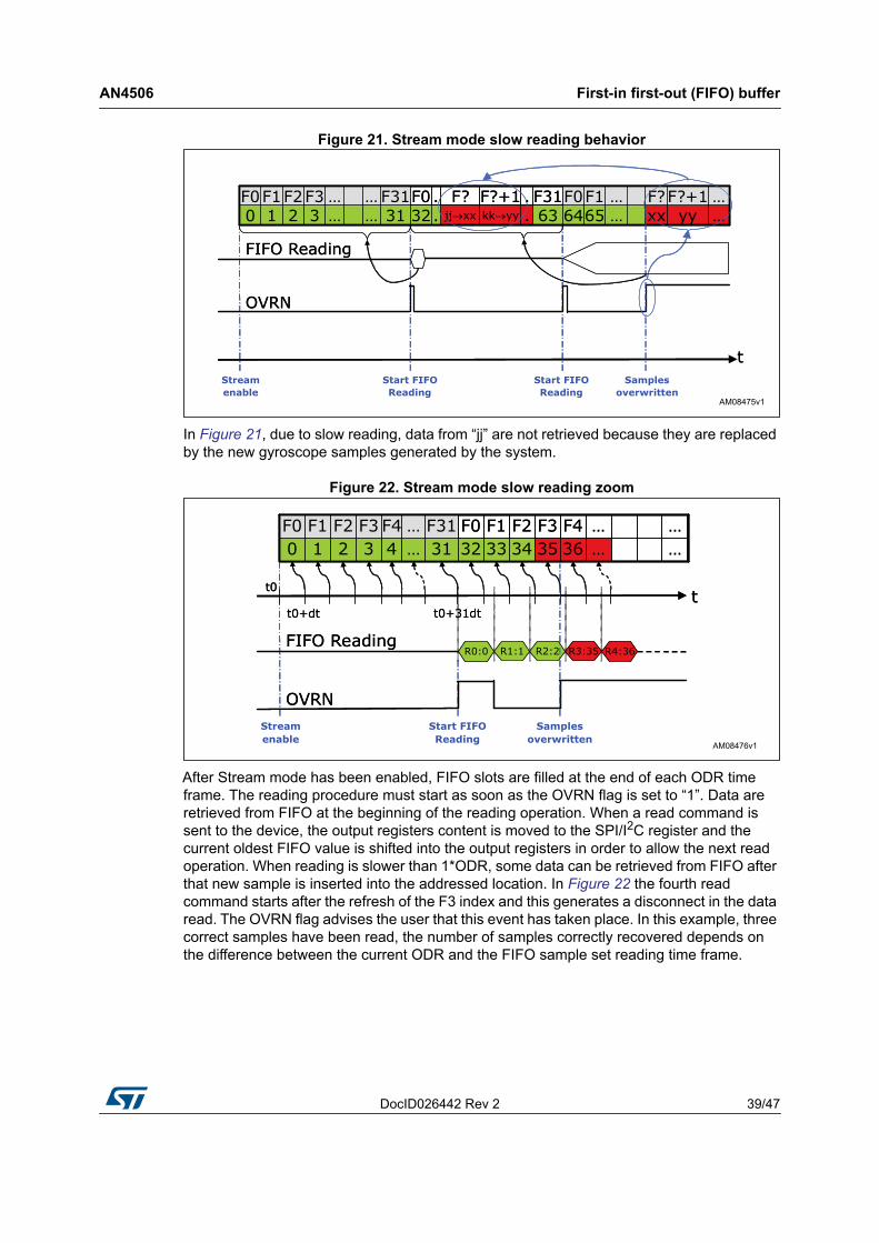
Figure 21. Stream mode slow reading behavior
In Figure 21, due to slow reading, data from “jj” are not retrieved because they are replaced by the new gyroscope samples generated by the system.
Figure 22. Stream mode slow reading zoom
After Stream mode has been enabled, FIFO slots are filled at the end of each ODR time frame. The reading procedure must start as soon as the OVRN flag is set to “1”. Data are retrieved from FIFO at the beginning of the reading operation. When a read command is sent to the device, the output registers content is moved to the SPI/I2C register and the current oldest FIFO value is shifted into the output registers in order to allow the next read operation. When reading is slower than 1*ODR, some data can be retrieved from FIFO after that new sample is inserted into the addressed location. In Figure 22 the fourth read command starts after the refresh of the F3 index and this generates a disconnect in the data read. The OVRN flag advises the user that this event has taken place. In this example, three correct samples have been read, the number of samples correctly recovered depends on the difference between the current ODR and the FIFO sample set reading time frame.
AM08475v1
tStreamenable
OVRN
FIFO Reading
Start FIFOReading
Start FIFOReading
.
.…yyxx…656463.kk→yyjj→xx3231……3210…F?+1F?…F1F0F31.F?+1F?F0F31……F3F2F1F0
Samplesoverwritten
t
OVRN
FIFO Reading
.
.…yyxx…656463.kk→yyjj→xx3231……3210…F?+1F?…F1F0F31.F?+1F?F0F31……F3F2F1F0
AM08476v1
Streamenable
t
OVRN
R0:0FIFO Reading
Start FIFOReading
Samplesoverwritten
……363534333231…43210……F4F3F2F1F0F31…F4F3F2F1F0
R1:1 R2:2 R3:35 R4:36
t0
t0+dt t0+31dtt
OVRN
R0:0FIFO Reading
……363534333231…43210……F4F3F2F1F0F31…F4F3F2F1F0
R1:1 R2:2 R3:35 R4:36
t0
t0+dt t0+31dt
First-in first-out (FIFO) buffer AN4506
40/47 DocID026442 Rev 2
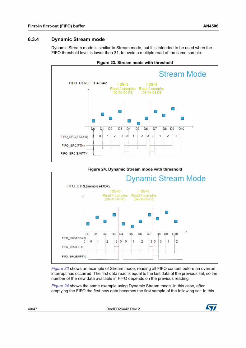
6.3.4 Dynamic Stream modeDynamic Stream mode is similar to Stream mode, but it is intended to be used when the FIFO threshold level is lower than 31, to avoid a multiple read of the same sample.
Figure 23. Stream mode with threshold
Figure 24. Dynamic Stream mode with threshold
Figure 23 shows an example of Stream mode, reading all FIFO content before an overrun interrupt has occurred. The first data read is equal to the last data of the previous set, so the number of the new data available in FIFO depends on the previous reading.
Figure 24 shows the same example using Dynamic Stream mode. In this case, after emptying the FIFO the first new data becomes the first sample of the following set. In this
AN4506 First-in first-out (FIFO) buffer
DocID026442 Rev 2 41/47
way, the number of new data available in the FIFO does not depend on the previous reading.
Follow these steps for Dynamic Stream mode configuration:1. Turn on FIFO by setting the FIFO_En bit to “1” in the CTRL5 register (0x24). After this
operation the FIFO buffer is enabled but is not collecting data, output registers are frozen to the last sample set loaded.
2. Activate Dynamic Stream mode by setting the FM[2:0] field to “110” in the FIFO_CTRL register (0x2E).
6.3.5 Stream-to-FIFO modeThis mode is a combination of the Stream and FIFO modes described above. In Stream-to-FIFO mode, the FIFO buffer starts operating in Stream mode and switches to FIFO mode when the selected interrupt occurs.
Follow these steps for Stream-to-FIFO mode configuration:1. Configure desired interrupt generator using register IG_CFG (0x30).2. Turn on FIFO by setting the FIFO_En bit to “1” in the CTRL5 register (0x24). After this
operation the FIFO buffer is enabled but is not collecting data, output registers are frozen to the last samples set loaded.
3. Activate Stream-to-FIFO mode by setting the FM[2:0] field to “011” in the FIFO control register (0x2E).
The interrupt trigger is related to the IA bit in the IG_SRC register and it is generated even if the interrupt signal is not driven to an interrupt pad. Switching modes is performed if both IA and OVRN bits are set high. Stream-to-FIFO mode is sensitive to the trigger level and not to the trigger edge; this means that if Stream-to-FIFO is in FIFO mode and the interrupt condition disappears, the FIFO buffer returns to Stream mode because the IA bit becomes zero. It is recommended to latch the interrupt signal used as the FIFO trigger in order to avoid losing interrupt events. If the selected interrupt is latched, it is necessary to read the register IG_SRC to clear the IA bit; after reading, the IA bit takes 2*ODR to go low.
In Stream mode the FIFO buffer continues filling, when the buffer is full, the OVRN bit is set high and the next samples overwrite the oldest. When trigger occurs, two different cases can be observed:1. If the FIFO buffer is already full (OVRN = “1”), it stops collecting data at the first sample
after the trigger. FIFO content is composed of #30 samples collected before the trigger event, the sample that has generated the interrupt event and one sample after trigger.
2. If FIFO is not full yet (initial transient), it continues filling until it is full (OVRN = “1”) and then, if trigger is still present, it stops collecting data.
First-in first-out (FIFO) buffer AN4506
42/47 DocID026442 Rev 2
Figure 25. Stream-to-FIFO mode: interrupt not latched
Figure 26. Stream-to-FIFO mode: interrupt latched
Stream-to-FIFO can be used in order to analyze the sample history that generates an interrupt; the standard operation is to read FIFO content when FIFO mode is triggered and FIFO buffer is full and stopped.
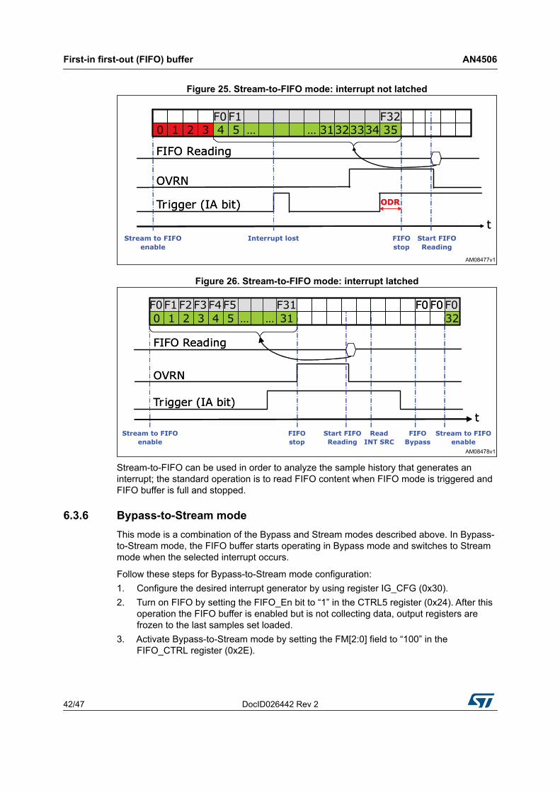
6.3.6 Bypass-to-Stream modeThis mode is a combination of the Bypass and Stream modes described above. In Bypass-to-Stream mode, the FIFO buffer starts operating in Bypass mode and switches to Stream mode when the selected interrupt occurs.
Follow these steps for Bypass-to-Stream mode configuration:1. Configure the desired interrupt generator by using register IG_CFG (0x30).2. Turn on FIFO by setting the FIFO_En bit to “1” in the CTRL5 register (0x24). After this
operation the FIFO buffer is enabled but is not collecting data, output registers are frozen to the last samples set loaded.
3. Activate Bypass-to-Stream mode by setting the FM[2:0] field to “100” in the FIFO_CTRL register (0x2E).
AN4506 First-in first-out (FIFO) buffer
DocID026442 Rev 2 43/47
The interrupt trigger is related to the IA bit in the IG_SRC register and it is generated even if the interrupt signal is not driven to an interrupt pad. Bypass-to-Stream mode is sensitive to the trigger level and not to the trigger edge; this means that if the FIFO buffer is in Stream mode and the interrupt condition disappears, the FIFO buffer returns to Bypass mode because the IA bit becomes zero.
It is recommended to latch the interrupt signal used as the stream trigger in order to avoid losing interrupt events. If the selected interrupt is latched, it is necessary to read the register IG_SRC to clear the IA bit; after reading, the IA bit takes 2*ODR to go low.
In Stream mode the FIFO buffer continues filling. When the buffer is full, the OVRN bit is set high and the next samples overwrite the oldest.
Figure 27. Bypass-to-Stream mode
Bypass-to-Stream can be used in order to start the acquisition when the configured interrupt is generated.
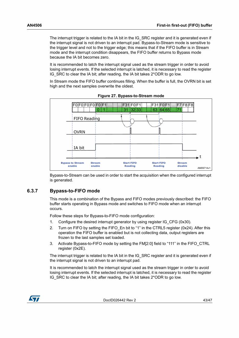
6.3.7 Bypass-to-FIFO modeThis mode is a combination of the Bypass and FIFO modes previously described: the FIFO buffer starts operating in Bypass mode and switches to FIFO mode when an interrupt occurs.
Follow these steps for Bypass-to-FIFO mode configuration:1. Configure the desired interrupt generator by using register IG_CFG (0x30).2. Turn on FIFO by setting the FIFO_En bit to “1” in the CTRL5 register (0x24). After this
operation the FIFO buffer is enabled but is not collecting data, output registers are frozen to the last samples set loaded.
3. Activate Bypass-to-FIFO mode by setting the FM[2:0] field to “111” in the FIFO_CTRL register (0x2E).
The interrupt trigger is related to the IA bit in the IG_SRC register and it is generated even if the interrupt signal is not driven to an interrupt pad.
It is recommended to latch the interrupt signal used as the stream trigger in order to avoid losing interrupt events. If the selected interrupt is latched, it is necessary to read the register IG_SRC to clear the IA bit; after reading, the IA bit takes 2*ODR to go low.
First-in first-out (FIFO) buffer AN4506
44/47 DocID026442 Rev 2
After the interrupt occurs and FIFO switches to FIFO mode, the buffer starts collecting data and fills all the 32 slots (from F0 to F31) at the selected output data rate. When the buffer is full, the OVRN bit goes up and data collection is permanently stopped; the user can read FIFO content. The reading procedure is composed of a 32 sample set of 6 bytes for a total of 192 bytes and retrieves data starting from the oldest sample stored in FIFO (F0). The OVRN bit is reset when the first sample set has been read.
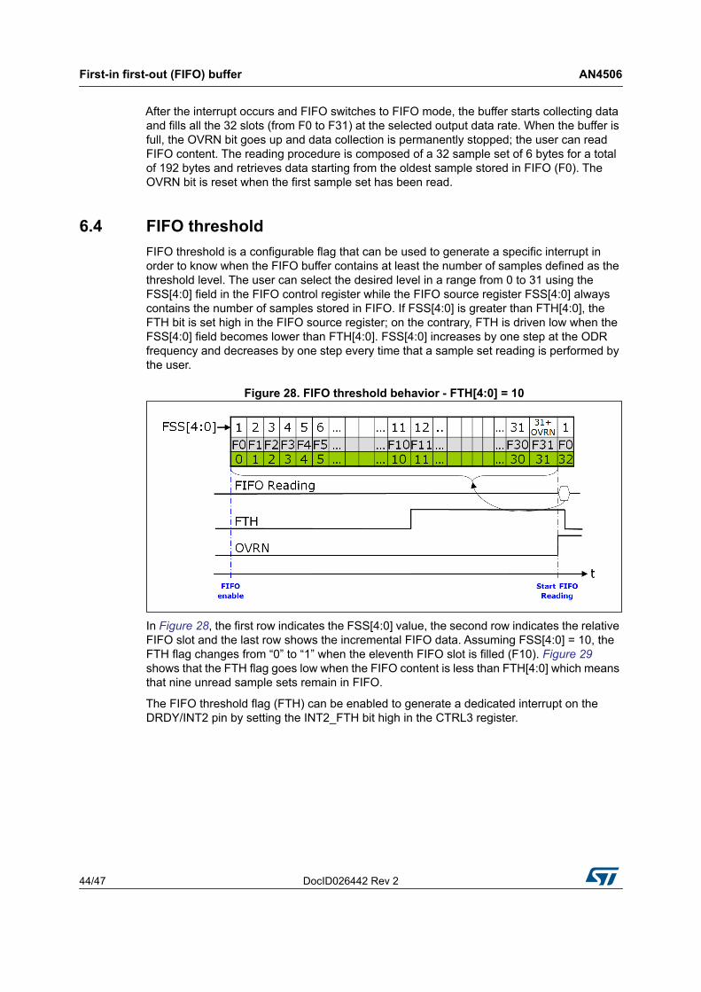
6.4 FIFO thresholdFIFO threshold is a configurable flag that can be used to generate a specific interrupt in order to know when the FIFO buffer contains at least the number of samples defined as the threshold level. The user can select the desired level in a range from 0 to 31 using the FSS[4:0] field in the FIFO control register while the FIFO source register FSS[4:0] always contains the number of samples stored in FIFO. If FSS[4:0] is greater than FTH[4:0], the FTH bit is set high in the FIFO source register; on the contrary, FTH is driven low when the FSS[4:0] field becomes lower than FTH[4:0]. FSS[4:0] increases by one step at the ODR frequency and decreases by one step every time that a sample set reading is performed by the user.
Figure 28. FIFO threshold behavior - FTH[4:0] = 10
In Figure 28, the first row indicates the FSS[4:0] value, the second row indicates the relative FIFO slot and the last row shows the incremental FIFO data. Assuming FSS[4:0] = 10, the FTH flag changes from “0” to “1” when the eleventh FIFO slot is filled (F10). Figure 29 shows that the FTH flag goes low when the FIFO content is less than FTH[4:0] which means that nine unread sample sets remain in FIFO.
The FIFO threshold flag (FTH) can be enabled to generate a dedicated interrupt on the DRDY/INT2 pin by setting the INT2_FTH bit high in the CTRL3 register.
AN4506 First-in first-out (FIFO) buffer
DocID026442 Rev 2 45/47
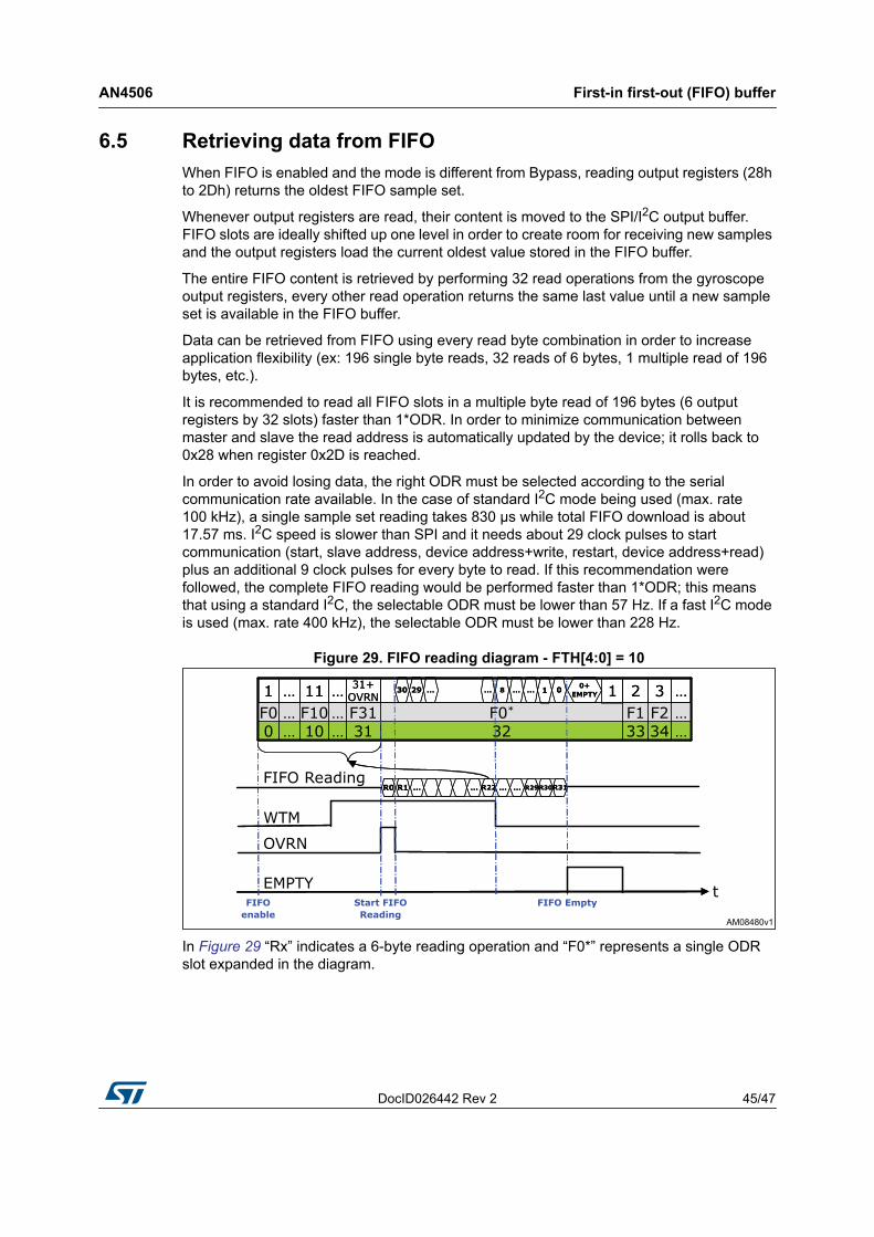
6.5 Retrieving data from FIFOWhen FIFO is enabled and the mode is different from Bypass, reading output registers (28h to 2Dh) returns the oldest FIFO sample set.
Whenever output registers are read, their content is moved to the SPI/I2C output buffer. FIFO slots are ideally shifted up one level in order to create room for receiving new samples and the output registers load the current oldest value stored in the FIFO buffer.
The entire FIFO content is retrieved by performing 32 read operations from the gyroscope output registers, every other read operation returns the same last value until a new sample set is available in the FIFO buffer.
Data can be retrieved from FIFO using every read byte combination in order to increase application flexibility (ex: 196 single byte reads, 32 reads of 6 bytes, 1 multiple read of 196 bytes, etc.).
It is recommended to read all FIFO slots in a multiple byte read of 196 bytes (6 output registers by 32 slots) faster than 1*ODR. In order to minimize communication between master and slave the read address is automatically updated by the device; it rolls back to 0x28 when register 0x2D is reached.
In order to avoid losing data, the right ODR must be selected according to the serial communication rate available. In the case of standard I2C mode being used (max. rate 100 kHz), a single sample set reading takes 830 μs while total FIFO download is about 17.57 ms. I2C speed is slower than SPI and it needs about 29 clock pulses to start communication (start, slave address, device address+write, restart, device address+read) plus an additional 9 clock pulses for every byte to read. If this recommendation were followed, the complete FIFO reading would be performed faster than 1*ODR; this means that using a standard I2C, the selectable ODR must be lower than 57 Hz. If a fast I2C mode is used (max. rate 400 kHz), the selectable ODR must be lower than 228 Hz.
Figure 29. FIFO reading diagram - FTH[4:0] = 10
In Figure 29 “Rx” indicates a 6-byte reading operation and “F0*” represents a single ODR slot expanded in the diagram.
Temperature sensor AN4506
46/47 DocID026442 Rev 2
7 Temperature sensor
The L3GD20H is provided with an internal temperature sensor that is suitable for delta temperature measurement. Temperature data are generated with a frequency of 1 Hz and are stored inside the OUT_TEMP register in 2’s complement format with a sensitivity of -1 LSB/°C.
8 Revision history
Table 34. Document revision historyDate Revision Changes
18-Jun-2014 1 Initial release.
30-Apr-2015 2Updated Section 2.5: Switching modesUpdated Section 3.5: DEN functionUpdated Section 6.3: FIFO modes

AN4506
DocID026442 Rev 2 47/47
IMPORTANT NOTICE – PLEASE READ CAREFULLY
STMicroelectronics NV and its subsidiaries (“ST”) reserve the right to make changes, corrections, enhancements, modifications, and improvements to ST products and/or to this document at any time without notice. Purchasers should obtain the latest relevant information on ST products before placing orders. ST products are sold pursuant to ST’s terms and conditions of sale in place at the time of order acknowledgement.
Purchasers are solely responsible for the choice, selection, and use of ST products and ST assumes no liability for application assistance or the design of Purchasers’ products.
No license, express or implied, to any intellectual property right is granted by ST herein.
Resale of ST products with provisions different from the information set forth herein shall void any warranty granted by ST for such product.
ST and the ST logo are trademarks of ST. All other product or service names are the property of their respective owners.
Information in this document supersedes and replaces information previously supplied in any prior versions of this document.
© 2015 STMicroelectronics – All rights reserved


![EXPRESSION OF INTEREST [EOI] - geleservices.com · (RTGS) / Axis Bank Over-the-counter (OTC). ... 3.1.1.26 Device shall have 3 axis accelerometer and 3 axis gyroscope for getting](https://img.pdfslide.us/doc/110x75/5b595e257f8b9a4e1b8d23aa/expression-of-interest-eoi-rtgs-axis-bank-over-the-counter-otc-.jpg)