Embed Size (px)
Citation preview

L10: 6.111 Spring 2009 1Introductory Digital Systems Laboratory
L10: Analog Building Blocks
(OpAmps, A/D, D/A)
Acknowledgement: Dave Wentzloff
Lecture Notes prepared by Professor Anantha Chadrakasan

L10: 6.111 Spring 2009 2Introductory Digital Systems Laboratory
Introduction to Operational Amplifiers
Typically very high input resistance ~ 300KΩHigh DC gain (~105)Output resistance ~75Ω
DC Model
LM741 Pinout
inout VfaV ⋅= )(
a(f)
f10Hz
105-20dB/decade
+10 to +15V
-10 to -15V
idva ⋅idv
inRoutR+
−outv

L10: 6.111 Spring 2009 3Introductory Digital Systems Laboratory
The Inside of a 741 OpAmp
DifferentialInput Stage
AdditionalGain Stage Output Stage
Current Source for biasing
Bipolar versionhas small inputBias current
MOS OpAmpshave ~ 0 input current
Gain is Sensitive to Operating Condition (e.g., Device, Temperature, Power supply voltage, etc.)
Output devicesprovides largedrive current

L10: 6.111 Spring 2009 4Introductory Digital Systems Laboratory
Simple Model for an OpAmp
+
-
i+ ~ 0
i- ~ 0+
-
+-
vid
vout
vout
vid
VCC = 10V
-VCC = -10V
ε = 100μV
-100μV
Reasonable approximation
+
-vid
+- avid
+
-vout
Linear Mode
If -VCC < vout < VCC
+
-vid -VCC
+
-vou
t
Negative Saturation
vid < - ε
-+
+
-vid
+
-vou
t
Positive Saturation
vid > ε
-+ +VCC
-VCC
VCC
Small input range for “Open” loop Configuration

L10: 6.111 Spring 2009 5Introductory Digital Systems Laboratory
The Power of (Negative) Feedback
inv outv1R
2R
-+
-
+
vid+- avid
+
-vout
inv
R2
-+
R1
021
=+
++
Rvv
Rvv idoutidin
avv out
id = ⎥⎦
⎤⎢⎣
⎡++−=
2211
11RR
aRa
vRv outin
( ) ( )11 1
2
21
2 >>−≈++
−= aifRR
RRaaR
vv
in
out
Overall (closed loop) gain does not depend on open loop gainTrade gain for robustnessEasier analysis approach: “virtual short circuit approach”
v+ = v- = 0 if OpAmp is linear
+
-

L10: 6.111 Spring 2009 6Introductory Digital Systems Laboratory
Basic OpAmp Circuits
+
−
Voltage Follower (buffer) Non-inverting
Differential Input
invoutv
inout vv ≈
Integrator
+
-
inout vR
RRv1
21 +≈
( )121
2ininR
Rout vvv −≈ dtvv
t
inRCout ∫∞−
−≈ 1

L10: 6.111 Spring 2009 7Introductory Digital Systems Laboratory
Use With Open Loop
Analog Comparator:
Is V+ > V- ?The Output is a DIGITAL signal
LM311 is a single supplycomparator

L10: 6.111 Spring 2009 8Introductory Digital Systems Laboratory
Data Conversion: Quantization Noise
Quantization noise exists even with ideal A/D and D/A converters inv
noisev
LSB
A/D D/A
digitalcode
inv
Quantizationnoise
+−
00 01 10 1104refV
2refV4
3 refV
Binary code
Ana
log
Out
put
00
01
10
11
04refV
2refV
43 refV
Analog Input
Bin
ary
Out
put
refV
4refV
2refV
43 refV
refV
A/D Conversion D/A Conversion

L10: 6.111 Spring 2009 9Introductory Digital Systems Laboratory
Non-idealities in Data Conversion
Binary code
Ana
log
Ideal
Offseterror
Binary code
Ana
log
Ideal
Gainerror
Offset – a constant voltage offset that appears at the output when the digital input is 0
Gain error – deviation of slope from ideal value of 1
Binary code
Ana
log
Ideal
Integralnonlinearity
Integral Nonlinearity – maximum deviation from the ideal analog output voltage
Differential nonlinearity – the largest increment in analog output for a 1-bit change
Binary code
Ana
log Ideal
Non-monoticity
L10: 6.111 Spring 2009 10Introductory Digital Systems Laboratory
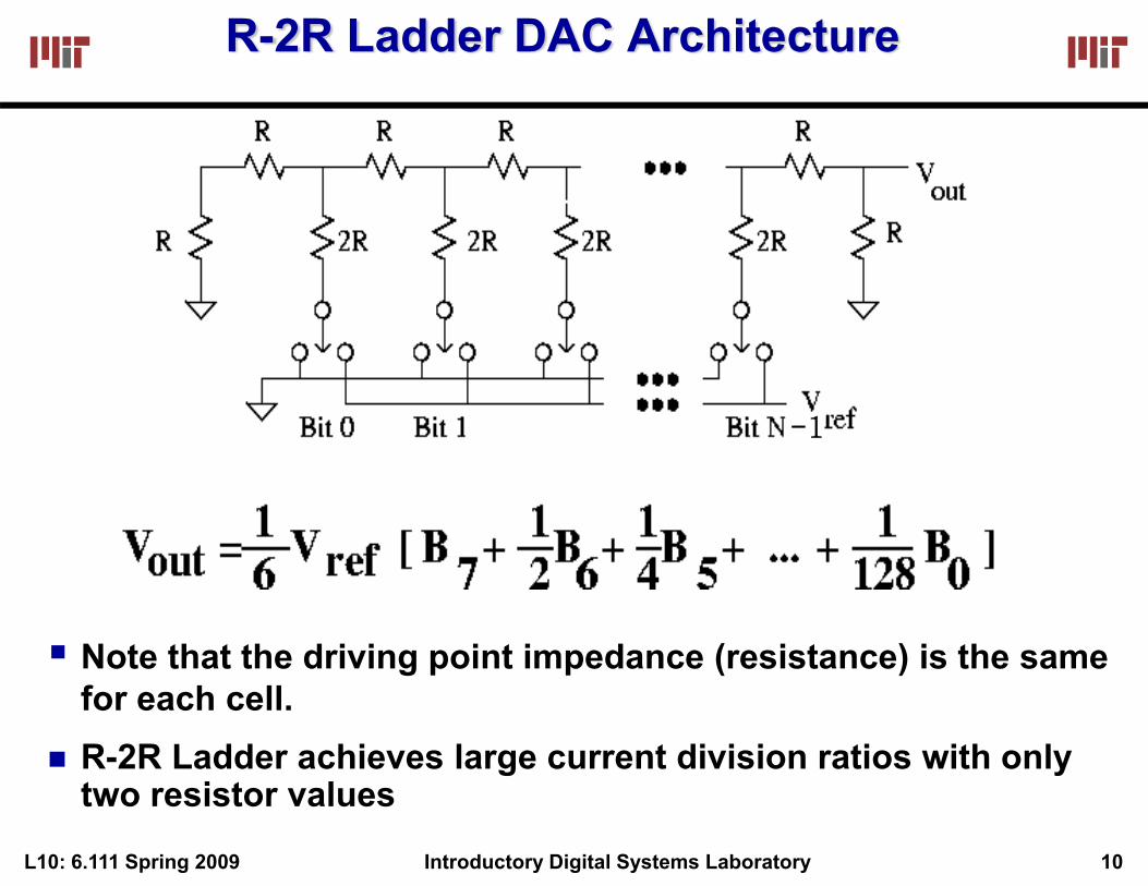
R-2R Ladder DAC Architecture
Note that the driving point impedance (resistance) is the same for each cell.R-2R Ladder achieves large current division ratios with only two resistor values
-1

L10: 6.111 Spring 2009 11Introductory Digital Systems Laboratory
DAC (AD 558) Specs
8-bit DACSingle Supply Operation: 5V to 15VIntegrates required references (bandgap voltage reference)Uses a R-2R resistor ladder Settling time 1μsProgrammable output range from0V to 2.56V or 0V to 10VSimple Latch based interface

L10: 6.111 Spring 2009 12Introductory Digital Systems Laboratory
Chip Architecture and Interface
CE CS
LATCHD[7:0]
Outputs are noisy when input bits settles, so it is best to have inputs stable before latching the input data

L10: 6.111 Spring 2009 13Introductory Digital Systems Laboratory
Setting the Voltage Range
Very similar to anon-inverting amp
Strap output fordifferent voltageranges
Convert data to Offset binary

L10: 6.111 Spring 2009 14Introductory Digital Systems Laboratory
Another Approach: Binary-Weighted DAC
Analog Devices AD9768 uses two banks of ratioed currentsAdditional current division performed by 750 Ω resistor between the two banks
Switch binary-weighted currentsMSB to LSB current ratio is 2N
AD9768
3b 2b 1b 0b
R
outv
( )08
114
122
13 bbbbIRvout
+++−=
+-
I2I I
4I8
Reference current source

L10: 6.111 Spring 2009 15Introductory Digital Systems Laboratory
Glitching and Thermometer D/A
Glitching is caused when switching times in a D/A are not synchronizedExample: Output changes from 011 to 100 – MSB switch is delayedFiltering reduces glitch but increases the D/A settling timeOne solution is a thermometer code D/A – requires 2N – 1 switches but no ratioed currents
100011→outv
t
Binary Thermometer0 0 0 0 00 1 0 0 11 0 0 1 11 1 1 1 1
0TI
R
outv
( )210 TTTIRvout ++−=
I I1T 2T

L10: 6.111 Spring 2009 16Introductory Digital Systems Laboratory
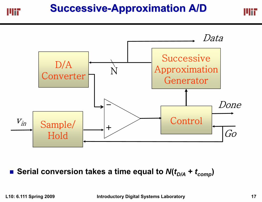
Successive-Approximation A/D
Example: 3-bit A/D conversion, 2 LSB < Vin < 3 LSB
D/A converters are typically compact and easier to design. Why not A/D convert using a D/A converter and a comparator?D to A generates analog voltage which is compared to the input voltageIf D to A voltage > input voltage then set that bit; otherwise, reset that bitThis type of A to D takes a fixed amount of time proportional to the bit length
Vin code
D/A
Comparatorout
C+ −
L10: 6.111 Spring 2009 17Introductory Digital Systems Laboratory
Successive-Approximation A/D
Serial conversion takes a time equal to N(tD/A + tcomp)
SuccessiveApproximation
Generator
Control
Done
Go
-
+Sample/Hold
D/AConverter
vin
N
Data
L10: 6.111 Spring 2009 18Introductory Digital Systems Laboratory
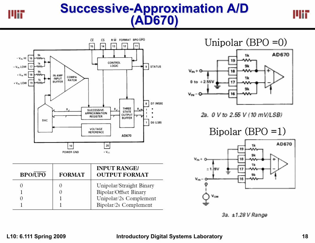
Successive-Approximation A/D (AD670)
~10μs conversion time
Unipolar (BPO =0)
Bipolar (BPO =1)

L10: 6.111 Spring 2009 19Introductory Digital Systems Laboratory
Single Write, Single Read Operation(see data sheet for other modes)
R/W
CE, CS
Data Data Valid
tw
Valid
tDC
tw (write/start pulse width) = 300ns (min)tDC (delay to start conversion) = 700ns (max)tc (conversion time) = 10ms (max)tTD (Bus Access Time) = 250 (max)tDT (Output Float Delay) = 150 (max)
tc tTDtDT
Write
Read
Control bits CE and CS can be wired to ground if A/D is the only chip driving the busSuggestion: tie CE and CS pins together and hardwire BPO and Format
Status

L10: 6.111 Spring 2009 20Introductory Digital Systems Laboratory
Simple A/D Interface FSM
Data[7:0]
STATUS
CS
CE
AD670
cs_b
R/W r_w_b
FSM
clk
reset
sample
DQ
dataavail
status
Status should be synchronized: why?
Courtesy of James Oey and Cemal Akcaba

L10: 6.111 Spring 2009 21Introductory Digital Systems Laboratory
2/5
Example A/D Verilog Interface
module AD670 (clk, reset, sample, dataavail, r_wbar, cs_bar, status, state);
// System Clkinput clk; // Global Reset signal, assume it is synchronized
input reset;
// User Interface input sample; output dataavail;
// A-D Interfaceinput status;reg status_d1, status_d2;output r_wbar, cs_bar;output [3:0] state;
// internal state reg [3:0] state;reg [3:0] nextstate;reg r_wbar_int, r_wbar;reg cs_bar_int, cs_bar;reg dataavail;
// State declarations.parameter IDLE = 0;parameter CONV0 = 1;parameter CONV1 = 2;parameter CONV2 = 3;parameter WAITSTATUSHIGH = 4;parameter WAITSTATUSLOW = 5;parameter READDELAY0 = 6;parameter READDELAY1 = 7;parameter READCYCLE = 8;
always @ (posedge clk or negedge reset) begin
if (!reset) state <=IDLE;else begin state <=nextstate;
status_d1 <= status;status_d2 <= status_d1;
r_wbar <= r_wbar_int;cs_bar <=cs_bar_int;
endend1/5

L10: 6.111 Spring 2009 22Introductory Digital Systems Laboratory
3/5
Example A/D Verilog Interface (cont.)
always @ (state or status_d2 or sample) begin// defaultsr_wbar_int = 1; cs_bar_int = 1; dataavail = 0;
case (state)
IDLE: beginif(sample) nextstate = CONV0;else nextstate = IDLE;end
CONV0:begin
r_wbar_int = 0; cs_bar_int = 0; nextstate = CONV1;
end
CONV1:begin
r_wbar_int = 0; cs_bar_int = 0; nextstate = CONV2;
end
CONV2:begin
r_wbar_int = 0; cs_bar_int = 0; nextstate = WAITSTATUSHIGH;
end WAITSTATUSHIGH:begin
cs_bar_int = 0; if (status_d2) nextstate = WAITSTATUSLOW;
else nextstate = WAITSTATUSHIGH;end
WAITSTATUSLOW:begin
cs_bar_int = 0; if (!status_d2) nextstate = READDELAY0;else nextstate = WAITSTATUSLOW;
end
4/5

L10: 6.111 Spring 2009 23Introductory Digital Systems Laboratory
Example A/D Verilog Interface(cont.)
READDELAY0:begin
cs_bar_int = 0; nextstate = READDELAY1;
end
READDELAY1:begin
cs_bar_int = 0; nextstate = READCYCLE;
end
READCYCLE:begin
cs_bar_int = 0; dataavail = 1;nextstate = IDLE;
end
default: nextstate = IDLE;endcase // case(state)
end // always @ (state or status_d2 or sample)endmodule // adcInterface
5/5

L10: 6.111 Spring 2009 24Introductory Digital Systems Laboratory
Simulation
On reset, present state goes to 0
Sample pulse initiates data conversion
Notice a one cycle delay since A/D control signal delayed through a register
r_w_b must stay low for at least 3 cycles (@ 100ns period)
Status is synchronized – two register delays
Wait for ~10ms for status to go low
Enable read flip-flop

L10: 6.111 Spring 2009 25Introductory Digital Systems Laboratory
Flash A/D Converter
Brute-force A/D conversionSimultaneously compare the analog value with every possible reference valueFastest method of A/D conversionSize scales exponentially with precision(requires 2N comparators)
C+
−
C+
−
C+
−
R
R
refV inv
0b
1b
The
rmom
ete r
tobi
nary
ComparatorsR
R
Can be implemented as OpAmp in open loop

L10: 6.111 Spring 2009 26Introductory Digital Systems Laboratory
AD 775 – Flash Data Converter

L10: 6.111 Spring 2009 27Introductory Digital Systems Laboratory
High Performance Converters:Use Pipelining and Parallelism!
Sample/Hold
−
+
Amplifier1-bit
A/DConverter
D/AConverter 2 Sample/
Hold
−
+
Amplifier1-bit
A/DConverter
D/AConverter 2 …
Pipelining (used in video rate, RF basestations, etc.)
Parallelism (use many slower A/D’s in parallel to build veryhigh speed A/D converters)
[ISSCC 2003],Poulton et. al.
20Gsample/sec,8-bit ADCfrom Agilent Labs

L10: 6.111 Spring 2009 28Introductory Digital Systems Laboratory
Summary of Analog Blocks
Analog blocks are integral components of any system. Need data converters (analog to digital and digital to analog), analog processing (OpAmps circuits, switched capacitors filters, etc.), power converters (e.g., DC-DC conversion), etc.We looked at example interfaces for A/D and D/A converters
Make sure you register critical signals (enables, R/W, etc.)
Analog design incorporate digital principlesGlitch free operation using codingParallelism and Pipelining!More advanced concepts such as calibration