Embed Size (px)
Citation preview
© 2016 Freescale Semiconductor, Inc. All rights reserved.
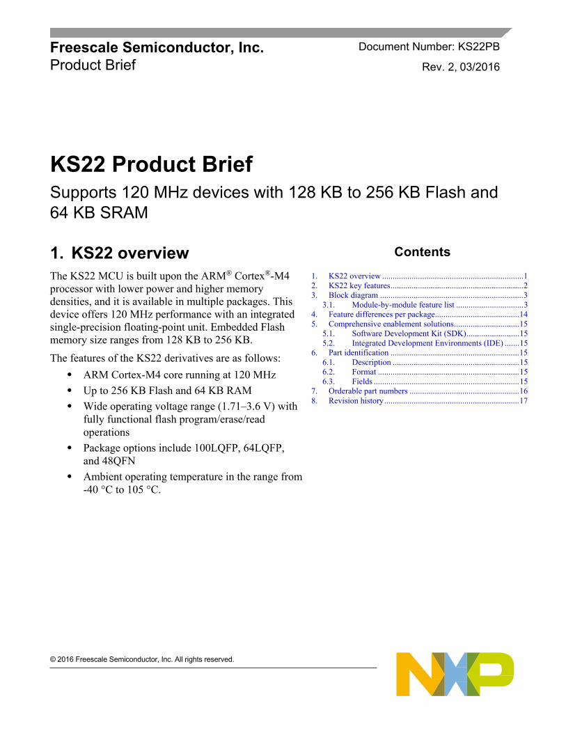
KS22 Product Brief Supports 120 MHz devices with 128 KB to 256 KB Flash and 64 KB SRAM
1. KS22 overview The KS22 MCU is built upon the ARM® Cortex®-M4 processor with lower power and higher memory densities, and it is available in multiple packages. This device offers 120 MHz performance with an integrated single-precision floating-point unit. Embedded Flash memory size ranges from 128 KB to 256 KB.
The features of the KS22 derivatives are as follows: • ARM Cortex-M4 core running at 120 MHz • Up to 256 KB Flash and 64 KB RAM • Wide operating voltage range (1.71–3.6 V) with
fully functional flash program/erase/read operations
• Package options include 100LQFP, 64LQFP, and 48QFN
• Ambient operating temperature in the range from -40 °C to 105 °C.
Freescale Semiconductor, Inc. Document Number: KS22PB
Product Brief Rev. 2 , 03/2016
Contents 1. KS22 overview ................................................................... 1 2. KS22 key features ............................................................... 2 3. Block diagram .................................................................... 3
3.1. Module-by-module feature list ................................ 3 4. Feature differences per package ........................................ 14 5. Comprehensive enablement solutions ............................... 15
5.1. Software Development Kit (SDK) ......................... 15 5.2. Integrated Development Environments (IDE) ....... 15
6. Part identification ............................................................. 15 6.1. Description ............................................................ 15 6.2. Format ................................................................... 15 6.3. Fields ..................................................................... 15
7. Orderable part numbers .................................................... 16 8. Revision history ................................................................ 17
KS22 key features
KS22 Product Brief, Rev. 2, 03/2016 2 Freescale Semiconductor, Inc.
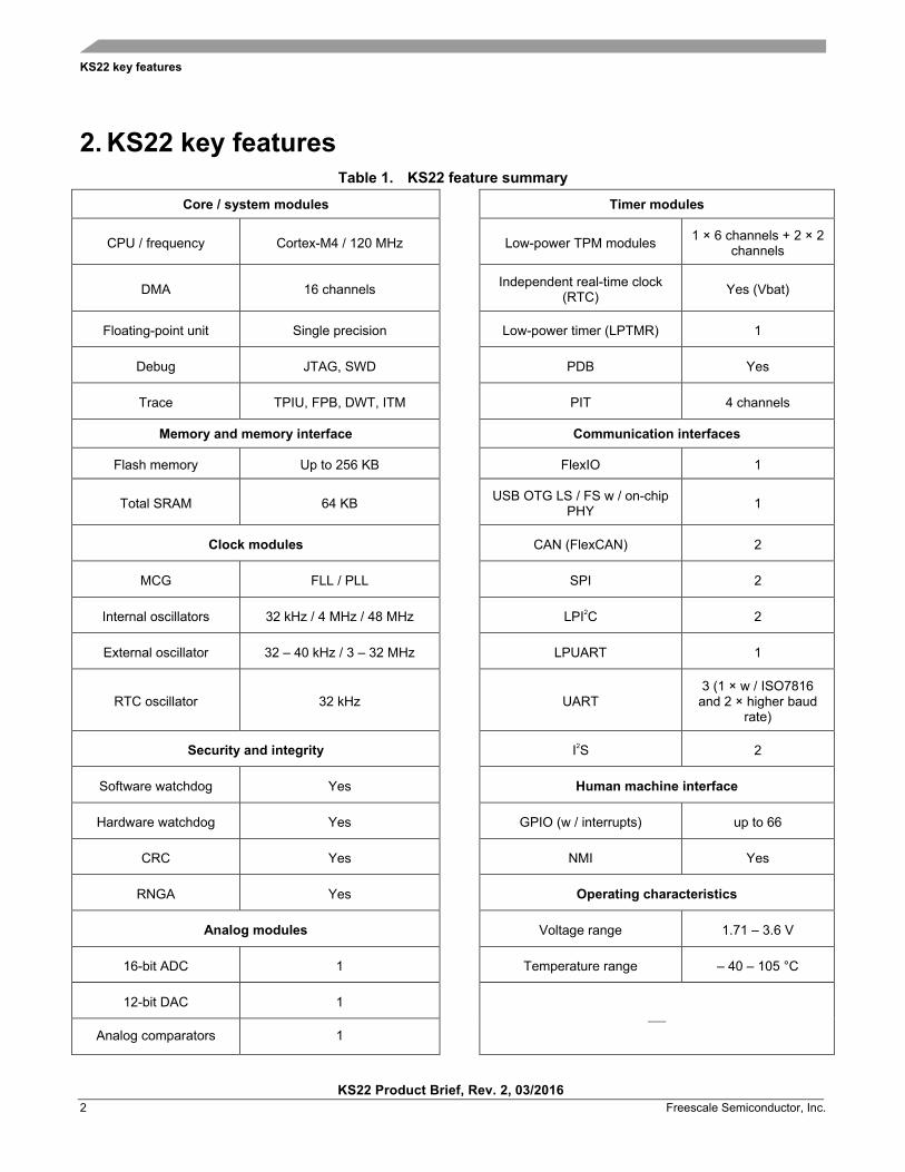
2. KS22 key features Table 1. KS22 feature summary
Core / system modules Timer modules
CPU / frequency Cortex-M4 / 120 MHz Low-power TPM modules 1 × 6 channels + 2 × 2 channels
DMA 16 channels Independent real-time clock (RTC) Yes (Vbat)
Floating-point unit Single precision Low-power timer (LPTMR) 1
Debug JTAG, SWD PDB Yes
Trace TPIU, FPB, DWT, ITM PIT 4 channels
Memory and memory interface Communication interfaces
Flash memory Up to 256 KB FlexIO 1
Total SRAM 64 KB USB OTG LS / FS w / on-chip PHY 1
Clock modules CAN (FlexCAN) 2
MCG FLL / PLL SPI 2
Internal oscillators 32 kHz / 4 MHz / 48 MHz LPI2C 2
External oscillator 32 – 40 kHz / 3 – 32 MHz LPUART 1
RTC oscillator 32 kHz UART 3 (1 × w / ISO7816
and 2 × higher baud rate)
Security and integrity I2S 2
Software watchdog Yes Human machine interface
Hardware watchdog Yes GPIO (w / interrupts) up to 66
CRC Yes NMI Yes
RNGA Yes Operating characteristics
Analog modules Voltage range 1.71 – 3.6 V
16-bit ADC 1 Temperature range – 40 – 105 °C
12-bit DAC 1 —
Analog comparators 1
Block diagram
KS22 Product Brief, Rev. 2, 03/2016 Freescale Semiconductor, Inc. 3
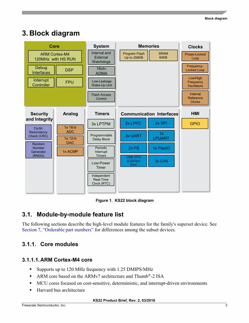
3. Block diagram
FPU32-byte
Register File
DebugInterfaces DSP
InterruptController
ARM Cortex-M4120MHz with HS RUN
Internal and External
Watchdogs
16ch-ADMA
Low-LeakageWake-Up Unit
Program FlashUp to 256KB
SRAM64KB
Phase-LockedLoop
Frequency-Locked Loop
Low/HighFrequencyOscillators
InternalReference
Clocks
CyclicRedundancyCheck (CRC)
3x LPTPM
ProgrammableDelay Block
PeriodicInterruptTimers
Low-PowerTimer
IndependentReal-Time
Clock (RTC)
2x I2S
2x SPI
3x UART
GPIO
Core System Memories Clocks
Securityand Integrity
Analog Timers Communication Interfaces HMI
USB OTG(LS/FS)+
PHY
2x LPI2C
1x LPUART
1x 16-b ADC
1x 12-b DAC
2x CAN
Flash Access Control
1x FlexIO
FPU
1x ACMP
Random Number
Generator (RNGA)
Figure 1. KS22 block diagram
3.1. Module-by-module feature list The following sections describe the high-level module features for the family's superset device. See Section 7, “Orderable part numbers” for differences among the subset devices.
3.1.1. Core modules
3.1.1.1. ARM Cortex-M4 core • Supports up to 120 MHz frequency with 1.25 DMIPS/MHz • ARM core based on the ARMv7 architecture and Thumb®-2 ISA • MCU cores focused on cost-sensitive, deterministic, and interrupt-driven environments • Harvard bus architecture
Block diagram
KS22 Product Brief, Rev. 2, 03/2016 4 Freescale Semiconductor, Inc.
• Three-stage pipeline with branch speculation • Integrated bus matrix • Integrated Digital Signal Processor (DSP) • Configurable Nested Vectored Interrupt Controller (NVIC) • Advanced configurable debug component • Single-Precision Floating-Point Unit (SPFPU)
3.1.1.2. Nested Vectored Interrupt Controller (NVIC) • Close coupling with Cortex-M4 core's Harvard architecture enables low-latency interrupt
handling • Up to 120 interrupt sources • Includes a single non-maskable interrupt • 16 levels of priority, with each interrupt source being dynamically configurable • Supports nesting of interrupts when higher-priority interrupts are activated • Relocatable vector table
3.1.1.3. Wakeup Interrupt Controller (WIC) • Supports interrupt handling when system clocking is disabled in low-power modes • Takes over and emulates the NVIC behavior when correctly primed by the NVIC on entering
deep sleep • A rudimentary interrupt-masking system with no prioritization logic signals for wakeup as soon
as non-masked interrupt is detected • Does not contain programmer’s model visible state, and is therefore invisible to end users, other
than through the benefits of reduced power consumption while sleeping
3.1.1.4. Debug controller • Serial-Wire JTAG Debug Port (SWJ-DP) combines
— External interface that provides a standard JTAG or cJTAG interface for debug access — External interface that provides a serial-wire bidirectional debug interface
• Debug Watchpoint and Trace (DWT) with the following functionality: — Four comparators configurable as hardware watchpoint, PC sampler event trigger, or data
address sampler event trigger — Several counters or data match event trigger for performance profiling — Configurable to emit PC samples at defined intervals, or to emit interrupt event
information • Instrumentation Trace Macrocell (ITM) with the following functionality:
— Software trace—writing directly to ITM stimulus registers can cause packet emitting
Block diagram
KS22 Product Brief, Rev. 2, 03/2016 Freescale Semiconductor, Inc. 5
— Hardware trace—packets generated by DWT are emitted by ITM — Time stamping—emitted relative to packets
• Test Port Interface Unit (TPIU) acts as a bridge between ITM and off-chip Trace Port Analyzer • Flash Patch and Breakpoints (FPB) implements hardware breakpoints, and patches code and data
from code space to system space
3.1.2. System modules
3.1.2.1. Power Management Control Unit (PMC) • Separate digital (regulated) and analog (referenced to digital) supply outputs • Programmable power-saving modes • No output supply decoupling capacitors required • Available wakeup from power-saving modes via RTC and external inputs • Integrated Power-On Reset (POR) • Integrated Low Voltage Detect (LVD) with reset (brownout) capability • Selectable LVD trip points • Programmable Low Voltage Warning (LVW) interrupt capability • Buffered bandgap reference voltage output • Factory-programmed trim for bandgap and LVD • 1 kHz Low-Power Oscillator (LPO)
3.1.2.2. DMA Channel Multiplexer (DMA MUX) • Up to 16 independently selectable DMA channel routers • Four periodic trigger sources available • Each channel router can be assigned to one of 63 possible peripheral DMA sources
3.1.2.3. DMA controller • Up to 16 fully programmable channels with 32-byte transfer control descriptors • Data movement via dual-address transfers for 8-bit, 16-bit, 32-bit, 128-bit, and 256-bit data
values • Programmable source and destination addresses, transfer size, and support for enhanced address
modes • Support for major and minor nested counters with one request and one interrupt per channel • Support for channel-to-channel linking and scatter/gather for continuous transfers with
fixed-priority and round-robin channel arbitration
Block diagram
KS22 Product Brief, Rev. 2, 03/2016 6 Freescale Semiconductor, Inc.
3.1.2.4. System clocks • Frequency-Locked Loop (FLL)
— Digitally-Controlled Oscillator (DCO) with programmable frequency range — Internal or external reference clock can be used to control the FLL — 0.2% resolution using 32 kHz internal reference clock
• Phase-Locked Loop (PLL) — Voltage-Controlled Oscillator (VCO) — External reference clock is used to control the PLL — Modulo VCO frequency divider phase/frequency detector — Integrated loop filter
• Internal reference clock generator — Can be used to control the FLL — Either slow or fast clock can be selected as the clock source for the MCU — Can be used as a clock source for other on-chip peripherals
• External clock from the Crystal Oscillator — Can be used to control the FLL and/or the PLL — Can be selected as the clock source for the MCU
• External clock monitor with reset request capability • Lock detector with interrupt request capability for use with the PLL • Auto Trim Machine (ATM) for trimming both slow and fast internal reference clocks • Multiple clock source options available for most peripherals
3.1.3. Memories and memory interfaces
3.1.3.1. On-chip memory • Up to 256 KB program Flash memory • 64 KB SRAM • Security circuitry to prevent unauthorized access to RAM and Flash contents
3.1.4. Security and integrity
3.1.4.1. Cyclic Redundancy Check (CRC) • Hardware CRC generator circuit using 16-bit/32-bit shift register • User-configurable 16-bit/32-bit CRC • Programmable generator polynomial • Error detection for all single-bit, double-bit, odd-bit, and most multi-bit errors
Block diagram
KS22 Product Brief, Rev. 2, 03/2016 Freescale Semiconductor, Inc. 7
• Programmable initial seed value • High-speed CRC calculation • Optional feature to transpose input data and CRC result via transpose register, required on
applications where bytes are in the LSB format
3.1.4.2. Watchdog Timer (WDOG) • Independent, configurable clock source input • Write-once control bits with unlock sequence • Programmable timeout period • Ability to test the Watchdog Timer and reset • Windowed refresh option • Robust refresh mechanism • Cumulative count of Watchdog resets between Power-On Resets • Configurable interrupt on timeout
3.1.4.3. External Watchdog Monitor (EWM) • Independent 1 kHz LPO clock source • Output signal to gate external circuit, which is controlled by CPU service or external input
3.1.4.4. Random Number Generator Accelerator (RNGA) • Supports the key-generation algorithm defined in the Digital Signature Standard
— http://www.itl.nist.gov/fipspubs/fip186.htm • Integrated entropy sources capable of providing the PRNG with entropy for its seed
3.1.5. Analog modules
3.1.5.1. 16-bit Analog-to-Digital Converter (ADC) • Linear successive approximation algorithm with up to 16-bit resolution • Output modes:
— Differential 16-bit, 13-bit, 11-bit, and 9-bit modes, in two’s complement 16-bit sign-extended format
— Single-ended 16-bit, 12-bit, 10-bit, and 8-bit modes, in right-justified unsigned format • Single or continuous conversion • Configurable sample time and conversion speed/power • Conversion complete and hardware average complete flag and interrupt • Input clock selectable from up to four sources
Block diagram
KS22 Product Brief, Rev. 2, 03/2016 8 Freescale Semiconductor, Inc.
• Operation in low-power modes for low noise • Asynchronous clock source for low-noise operation with an option to output the clock • Selectable asynchronous hardware conversion trigger with hardware channel select • Automatic compare with interrupt for various programmable values • Temperature sensor • Hardware average function • Self-calibration mode
3.1.5.2. High-Speed Analog Comparator (CMP) • 6-bit DAC programmable reference generator output • Up to seven selectable comparator inputs; each input can be compared with any input by any
polarity sequence • Selectable interrupt on rising edge, falling edge, or either rising or falling edges of the
comparator output • Comparator output supports:
— Sampled — Windowed (ideal for certain PWM zero-crossing-detection applications) — Digitally filtered using external sample signal or scaled peripheral clock
• Two performance modes: — Shorter propagation delay at the expense of higher power — Low power, with longer propagation delay
• Operational in all MCU power modes
3.1.5.3. 12-bit Digital-to-Analog Converter (DAC) • 12-bit resolution • On-chip programmable reference generator output. The voltage output range is from 1/4096 Vin
to Vin, and the step is 1/4096 Vin , where Vin is the input voltage • Vin can be selected from one reference source • Static operation in Normal Stop mode • 16-word data buffer supported with multiple operation modes • DMA support
Block diagram
KS22 Product Brief, Rev. 2, 03/2016 Freescale Semiconductor, Inc. 9
3.1.6. Timers
3.1.6.1. Programmable Delay Block (PDB) • Up to 15 trigger input sources and software trigger sources • One configurable PDB channel for ADC hardware trigger
— One trigger output for ADC hardware trigger, and up to two pre-trigger outputs for ADC trigger select per PDB channel
— One 16-bit delay register per pre-trigger output — Optional bypass of the pre-trigger outputs’ delay registers — Operation in One-Shot or Continuous modes — Optional Back-To-Back mode operation, which enables the ADC conversions completely
to trigger the next PDB channel • One DAC interval trigger
— One interval trigger output for DAC — One 16-bit delay interval register — Optional bypass of the delay interval trigger registers — Optional external triggers
• Up to eight pulse outputs (pulse-outs) — Pulse-outs can be enabled or disabled independently — Programmable pulse width
• DMA support
3.1.6.2. LPTPM • TPM clock mode is selectable
— It can increment on every edge of the asynchronous counter clock — It can increment on the rising edge of an external clock input synchronized to the
asynchronous counter clock • Prescaler can divide by 1, 2, 4, 8, 16, 32, 64, or 128 • TPM includes a 16-bit counter
— It can be a free-running counter or a modulo counter — The counting can be either up or up-down
• Includes six channels that can be configured for input capture, output compare, edge-aligned PWM mode, or center-aligned PWM mode
• Supports the generation of interrupt and/or DMA requests when the counter overflows (per channel)
• Supports selectable trigger input to reset the counter, or to make it start incrementing
Block diagram
KS22 Product Brief, Rev. 2, 03/2016 10 Freescale Semiconductor, Inc.
• Supports the generation of hardware triggers when the counter overflows (per channel)
3.1.6.3. Periodic Interrupt Timers (PITs) • Up to four general-purpose interrupt timers • Up to four interrupt timers for triggering of ADC conversions • 32-bit counter resolution • Clocked by the bus clock • DMA support • Two timers can be cascaded to form a 64-bit timer
3.1.6.4. Low-Power Timer • Operates as timer or pulse counter • Selectable clock for prescaler / glitch filter • Configurable glitch filter or prescaler • Interrupt generated on timer compare • Hardware trigger generated on timer compare
3.1.6.5. Real-Time Clock (RTC) • Independent power supply, POR, and 32 kHz crystal oscillator • 32-bit second counter with 32-bit alarm • 16-bit prescaler with compensation • Register write protection
— Hard lock requires VBAT POR to enable write access — Soft lock requires system reset to enable write/read access
3.1.7. Communication interface
3.1.7.1. USB On-The-Go Module (FS/LS) • Complies with USB specification rev 2.0 • USB host mode
— Supports Enhanced-Host-Controller Interface (EHCI) — Enables direct connection of FS/LS devices without OHCI/UHCI companion controller — Supported by Linux and other commercially available operating systems
• USB device mode — Full-speed operation via the on-chip transceiver — Supports one upstream-facing port
Block diagram
KS22 Product Brief, Rev. 2, 03/2016 Freescale Semiconductor, Inc. 11
— Supports 16 programmable bidirectional USB endpoints, including endpoint 0 • Suspend mode/low power
— As a host, firmware can suspend individual devices or entire USB, and disable chip clocks for low-power operation
— Device supports low-power suspend — Remote wakeup supported for host and device — Integrated with the processor’s low-power modes
• Includes on-chip full-speed (12 Mbps) and low-speed (1.5 Mbps) transceivers • A configurable connection, enabling any UART transmit and receive pins to be connected to the
full-speed USB physical layer
3.1.7.2. Serial Peripheral Interface (SPI) • Full-duplex three-wire synchronous transfers • Master mode or Slave mode • Data streaming operation in Slave mode with continuous slave selection • Buffered transmit/receive operation using the Transmit/Receive First-In First-Out (TX/RX
FIFO) with a depth of four entries • Programmable transfer attributes on a per-frame basis • Multiple Peripheral Chip Select (PCS) (six PCS are available for SPI0 and four PCS for SPI1),
expandable to 64 with external demultiplexer • Deglitching support for up to 32 Peripheral Chip Selects (PCSes) with external demultiplexer • DMA support for adding entries to TX FIFO, and removing entries from RX FIFO • Global interrupt request line • Modified SPI transfer formats for communication with slower peripheral devices • Power-saving architectural features
3.1.7.3. Low-Power Inter-Integrated Circuit (LPI2C) • Standard, Fast, Fast+, and Ultra Fast modes are supported • HS mode supported in Slave mode • Multi-master support including synchronization and arbitration • Clock stretching • General-call, 7-bit, and 10-bit addressing • Software reset, START byte, and Device ID require software support
Block diagram
KS22 Product Brief, Rev. 2, 03/2016 12 Freescale Semiconductor, Inc.
3.1.7.4. UART • Full-duplex operation • 13-bit baud rate selection with /32 fractional divide, based on the module clock frequency • Programmable 8-bit or 9-bit data formats • Programmable transmitter output polarity • Programmable receive input polarity • Up to 14-bit break character transmission • 11-bit break character detection option • Two receiver wakeup methods with idle line or address mark wakeup • Address match feature in the receiver to reduce address mark wakeup ISR overhead • Ability to select MSB or LSB to be the first bit on wire • UART0 supporting ISO-7816 protocol to interface with SIM cards and smart cards • Receiver framing error detection • Hardware parity generation and checking • 1/16 bit-time noise detection • DMA interface
3.1.7.5. LPUART • Full-duplex, standard Non-Return-to-Zero (NRZ) format • Programmable baud rates (13-bit modulo divider) with configurable oversampling ratio from 4×
to 32× • Transmit and receive baud rate can operate asynchronously to the bus clock:
— Baud rate can be configured independently of the bus clock frequency — Supports operation in Stop modes
• Interrupt, DMA, or polled operation: • Hardware parity generation and checking • Programmable 8-bit, 9-bit, or 10-bit character length • Programmable 1-bit or 2-bit stop bits • Three receiver wakeup methods:
— Idle line wakeup — Address mark wakeup — Receive data match
• Automatic address matching to reduce ISR overhead: — Address mark matching — Idle line address matching — Address match start, address match end
• Optional 13-bit break character generation/11-bit break character detection
Block diagram
KS22 Product Brief, Rev. 2, 03/2016 Freescale Semiconductor, Inc. 13
• Configurable idle length detection supporting 1, 2, 4, 8, 16, 32, 64, or 128 idle characters • Selectable transmitter output and receiver input polarity
3.1.7.6. Synchronous Serial Interface (I2S) • Independent (asynchronous) or shared (synchronous) transmit and receive sections with separate
or shared internal/external clocks and frame syncs, operating in Master or Slave modes, intended for audio support
• Master or Slave mode operation • Normal mode operation using frame sync • Network mode operation, enabling multiple devices to share the port with up to 32 time slots • Programmable data interface modes, such as I2S, LSB-aligned, and MSB-aligned • Programmable word length (8, 10, 12, 16, 18, 20, 22, or 24 bits) • AC97 support
3.1.7.7. FlexCAN • Full implementation of the CAN protocol specification (version 2.0B) • Flexible mailboxes with data length of 0–8 B • Each mailbox is configurable as RX or TX, all supporting standard and extended messages • Individual RX mask registers per mailbox • Fully-featured RX FIFO with storage capacity of up to six frames, and automatic internal pointer
handling • Transmission abort capability • Programmable clock source for the CAN Protocol Interface, either the bus clock or the crystal
oscillator • Unused structures’ space can be used as general-purpose RAM space • Listen-Only mode capability • Programmable Loop-Back mode supporting self-test operation • Programmable transmission priority scheme: lowest ID, lowest buffer number, or highest priority • Time Stamp based on 16-bit free-running timer • Global network time, synchronized by a specific message • Maskable interrupts • Independent of the transmission medium (an external transceiver is assumed) • Short latency time due to an arbitration scheme for high-priority messages • Low-power modes, with programmable wakeup on bus activity
Feature differences per package
KS22 Product Brief, Rev. 2, 03/2016 14 Freescale Semiconductor, Inc.
3.1.7.8. FlexIO The FlexIO module is capable of supporting a wide range of protocols including, but not limited to:
• UART • I2C • SPI • I2S • PWM/waveform generation
The following key features are provided: • Array of 32-bit shift registers with transmit, receive, and data match modes • Double-buffered shifter operation for continuous data transfer • Shifter concatenation to support large transfer sizes • Automatic start/stop bit generation • Interrupt, DMA, or polled transmit/receive operation • Programmable baud rates independent of bus clock frequency, with support for asynchronous
operation during Stop modes • Highly flexible 16-bit timers with support for a variety of internal or external trigger, reset,
enable, and disable conditions
3.1.8. Human-machine interface
3.1.8.1. General-Purpose Input/Output (GPIO) • Programmable glitch filter and interrupt with selectable polarity on selected input pins • Hysteresis and configurable pull up/pull down device on all input pins • Configurable slew rate on all output pins • Configurable drive strength on selected output pins • Independent pin value register to read logic level on digital pin
4. Feature differences per package Table 2. Feature differences per package
Package 64LQFP 100LQFP 48QFN Flash Up to 256 KB Up to 256 KB Up to 256 KB SRAM
64 KB 64 KB 64 KB
Total GPIOs 40 66 35
GPIOs with interrupt 40 66 35
High-drive GPIOs 8 8 8
Part identification
KS22 Product Brief, Rev. 2, 03/2016 Freescale Semiconductor, Inc. 15
5. Comprehensive enablement solutions
5.1. Software Development Kit (SDK) • Extensive suite of robust peripheral drivers, stacks, and middleware • Includes software examples demonstrating the usage of peripheral drivers, middleware,
and FreeRTOS
5.2. Integrated Development Environments (IDE) • Freescale Kinetis Design Studio IDE
— No-cost Integrated Development Environment (IDE) for Kinetis MCUs — Eclipse and GCC-based IDE for C/C++ editing, compiling, and debugging
• IAR Embedded Workbench® iar.com/kinetis • ARM Keil® Microcontroller Development Kit keil.com/freescale • Atollic® TrueSTUDIO® atollic.com/index.php/partnerfreescale • Broad ARM ecosystem support through Freescale Connect partners
6. Part identification
6.1. Description The chip part numbers have fields that identify the specific part. You can use the values of these fields to determine the specific part you have received.
6.2. Format The device part numbers have the following format: Q KS## A FFF T PP CC (N)
6.3. Fields The following table lists the possible values for each field in the part number. However, not all combinations are valid.
Orderable part numbers
KS22 Product Brief, Rev. 2, 03/2016 16 Freescale Semiconductor, Inc.
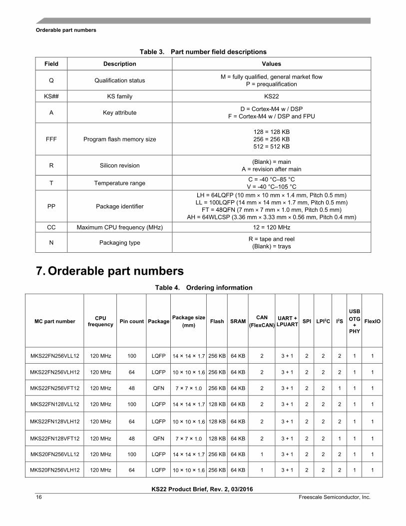
Table 3. Part number field descriptions
Field Description Values
Q Qualification status M = fully qualified, general market flow P = prequalification
KS## KS family KS22
A Key attribute D = Cortex-M4 w / DSP F = Cortex-M4 w / DSP and FPU
FFF Program flash memory size 128 = 128 KB 256 = 256 KB 512 = 512 KB
R Silicon revision (Blank) = main A = revision after main
T Temperature range C = -40 °C–85 °C V = -40 °C–105 °C
PP Package identifier
LH = 64LQFP (10 mm × 10 mm × 1.4 mm, Pitch 0.5 mm) LL = 100LQFP (14 mm × 14 mm × 1.7 mm, Pitch 0.5 mm)
FT = 48QFN (7 mm × 7 mm × 1.0 mm, Pitch 0.5 mm) AH = 64WLCSP (3.36 mm × 3.33 mm × 0.56 mm, Pitch 0.4 mm)
CC Maximum CPU frequency (MHz) 12 = 120 MHz
N Packaging type R = tape and reel (Blank) = trays
7. Orderable part numbers Table 4. Ordering information
MC part number CPU frequency Pin count Package
Package size (mm)
Flash SRAM CAN
(FlexCAN) UART + LPUART SPI LPI2C I2S
USB OTG
+ PHY
FlexIO
MKS22FN256VLL12 120 MHz 100 LQFP 14 × 14 × 1.7 256 KB 64 KB 2 3 + 1 2 2 2 1 1
MKS22FN256VLH12 120 MHz 64 LQFP 10 × 10 × 1.6 256 KB 64 KB 2 3 + 1 2 2 2 1 1
MKS22FN256VFT12 120 MHz 48 QFN 7 × 7 × 1.0 256 KB 64 KB 2 3 + 1 2 2 1 1 1
MKS22FN128VLL12 120 MHz 100 LQFP 14 × 14 × 1.7 128 KB 64 KB 2 3 + 1 2 2 2 1 1
MKS22FN128VLH12 120 MHz 64 LQFP 10 × 10 × 1.6 128 KB 64 KB 2 3 + 1 2 2 2 1 1
MKS22FN128VFT12 120 MHz 48 QFN 7 × 7 × 1.0 128 KB 64 KB 2 3 + 1 2 2 1 1 1
MKS20FN256VLL12 120 MHz 100 LQFP 14 × 14 × 1.7 256 KB 64 KB 1 3 + 1 2 2 2 1 1
MKS20FN256VLH12 120 MHz 64 LQFP 10 × 10 × 1.6 256 KB 64 KB 1 3 + 1 2 2 2 1 1
Revision history
KS22 Product Brief, Rev. 2, 03/2016 Freescale Semiconductor, Inc. 17
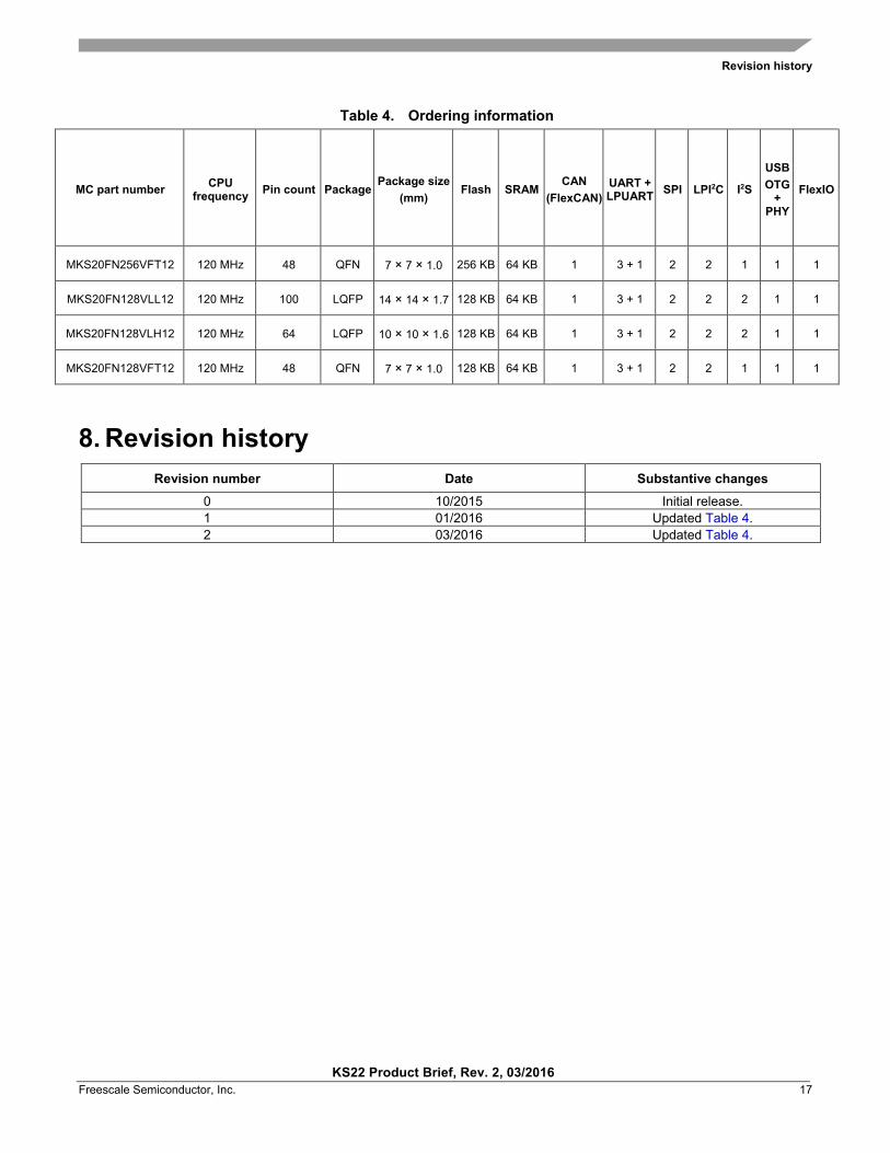
Table 4. Ordering information
MC part number CPU frequency Pin count Package
Package size (mm)
Flash SRAM CAN
(FlexCAN) UART + LPUART SPI LPI2C I2S
USB OTG
+ PHY
FlexIO
MKS20FN256VFT12 120 MHz 48 QFN 7 × 7 × 1.0 256 KB 64 KB 1 3 + 1 2 2 1 1 1
MKS20FN128VLL12 120 MHz 100 LQFP 14 × 14 × 1.7 128 KB 64 KB 1 3 + 1 2 2 2 1 1
MKS20FN128VLH12 120 MHz 64 LQFP 10 × 10 × 1.6 128 KB 64 KB 1 3 + 1 2 2 2 1 1
MKS20FN128VFT12 120 MHz 48 QFN 7 × 7 × 1.0 128 KB 64 KB 1 3 + 1 2 2 1 1 1
8. Revision history Revision number Date Substantive changes
0 10/2015 Initial release. 1 01/2016 Updated Table 4. 2 03/2016 Updated Table 4.
Document Number: KS22PB Rev. 2
03/2016
How to Reach Us:
Home Page: freescale.com
Web Support: freescale.com/support
Information in this document is provided solely to enable system and software implementers to use Freescale products. There are no express or implied copyright licenses granted hereunder to design or fabricate any integrated circuits based on the information in this document.
Freescale reserves the right to make changes without further notice to any products herein. Freescale makes no warranty, representation, or guarantee regarding the suitability of its products for any particular purpose, nor does Freescale assume any liability arising out of the application or use of any product or circuit, and specifically disclaims any and all liability, including without limitation consequential or incidental damages. “Typical” parameters that may be provided in Freescale data sheets and/or specifications can and do vary in different applications, and actual performance may vary over time. All operating parameters, including “typicals,” must be validated for each customer application by customer's technical experts. Freescale does not convey any license under its patent rights nor the rights of others. Freescale sells products pursuant to standard terms and conditions of sale, which can be found at the following address: freescale.com/SalesTermsandConditions.
Freescale, the Freescale logo, and Kinetis are trademarks of Freescale Semiconductor, Inc., Reg. U.S. Pat. & Tm. Off.
All other product or service names are the property of their respective owners. ARM, the ARM powered logo, and Cortex are registered trademarks of ARM Limited (or its subsidiaries) in the EU and/or elsewhere. mbed is a trademark of ARM Limited (or its subsidiaries) in the EU and/or elsewhere. All rights reserved.
© 2016 Freescale Semiconductor, Inc.