Embed Size (px)
Citation preview

1. Product profile
1.1 General description
The KMA210 is a magnetic angle sensor module. The MagnetoResistive (MR) sensor bridges, the mixed signal Integrated Circuit (IC) and the required capacitances are integrated into a single package.
This angular measurement module KMA210 is pre-programmed, pre-calibrated and therefore, ready to use.
The KMA210 allows user-specific adjustments of angular range, zero angle and clamping voltages. The settings are stored permanently in a non-volatile memory.
1.2 Features and benefits
KMA210Programmable angle sensorRev. 2 — 7 December 2011 Product data sheet
High precision sensor for magnetic angular measurement
High temperature range up to 160 C
Single package sensor module with integrated filters for improved ElectroMagnetic Compatibility (EMC)
Ratiometric analog output voltage
Automotive qualified in accordance with AEC-Q100 Rev-G
Overvoltage protection up to 16 V
Programmable user adjustments, including zero angle and angular range
Programming via One-Wire Interface (OWI)
Fail-safe non-volatile memory with write protection using lock bit
User-programmable 32-bit identifier
Independent from magnetic field strength above 35 kA/m
Magnet-loss, power-loss and broken bond wire detection
Ready to use without external components
Factory calibrated
NXP Semiconductors KMA210Programmable angle sensor
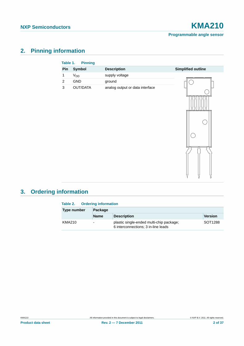
2. Pinning information
3. Ordering information
Table 1. Pinning
Pin Symbol Description Simplified outline
1 VDD supply voltage
2 GND ground
3 OUT/DATA analog output or data interface
1 2 3
Table 2. Ordering information
Type number Package
Name Description Version
KMA210 - plastic single-ended multi-chip package; 6 interconnections; 3 in-line leads
SOT1288
KMA210 All information provided in this document is subject to legal disclaimers. © NXP B.V. 2011. All rights reserved.
Product data sheet Rev. 2 — 7 December 2011 2 of 37
xxxx xxxxxxxxxxxxxxxxxxxxxxxxxxxxxx x xxxxxxxxxxxxxx xxxxxxxxxx xxx xxxxxx xxxxxxxxxxxxxxxxxxxxxxx xxxxxxxxxxxxxxxxxxxxxx xxxxx xxxxxx xx xxxxxxxxxxxxxxxxxxxxxxxxxxxxx xxxxxxxxxxxxxxxxxxxxxx xxxxxxxxxxx xxxxxxx xxxxxxxxxxxxxxxxxxx xxxxxxxxxxxxxxxx xxxxxxxxxxxxxx xxxxxx xx xxxxxxxxxxxxxxxxxxxxxxxxxxxxxxxx xxxxxxxxxxxxxxxxxxxxxxxx xxxxxxx xxxxxxxxxxxxxxxxxxxxxxxxxxxxxxxxxxxxxxxxxxxxxx xxxxxxxxxxx xxxxx x x
KM
A210
Pro
du
ct data sh
NX
P S
emico
nd
ucto
4. F
un
ction
al d
eet
rsK
MA
210P
rog
ramm
ab
le a
ng
le se
ns
or
iagram
ONE-WIREINTERFACE
SERIALINTERFACE
-LOSSTION
INTEGRATEDCAPACITANCES
CL
Cblock
VDD
OUT/DATA
GND
001aan661
All inform
ation provided in this docum
ent is subject to legal disclaim
ers.©
NX
P B
.V. 20
11. All rights reserved
.
Rev. 2 —
7 Decem
ber 2011
3 o
f 37 Fig 1. Functional diagram of KMA210
GND
POWER-LOSSDETECTION
ANGULARRANGE
ADJUSTMENT
ANGLECALCULATION
POWERDETEC
outputbuffer
DACADC
MU
LTIP
LEX
ER
(MU
X)
differentialamplifier
LOW-PASSFILTER
GND
LOW-PASSFILTER
OSCILLATOR
OFFSETCORRECTION
CLOCKGENERATOR
TESTCONTROL
ANALOGVOLTAGE
REGULATOR(CLEAN)
NON-VOLATILEMEMORY
MAGNETORESISTIVESENSOR BRIDGES SIGNAL CONDITIONING INTEGRATED CIRCUIT
DIGITALFILTER ANDAVERAGINGD
EM
UX
ANALOGVOLTAGE
REGULATOR(SWITCHING)
DIGITALVOLTAGE
REGULATORUNDERVOLTAGE
DETECTION/POR
POR

NXP Semiconductors KMA210Programmable angle sensor
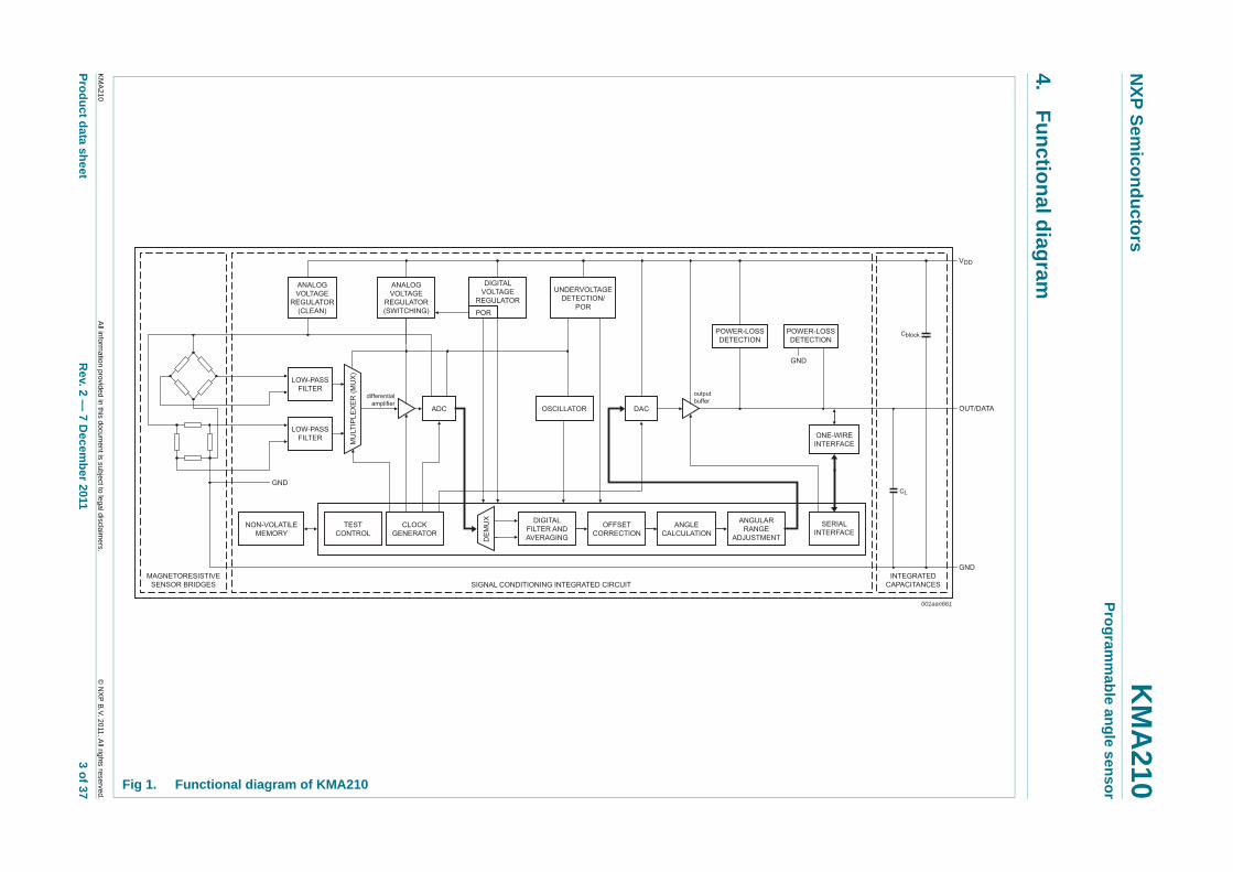
5. Functional description
The KMA210 amplifies two orthogonal differential signals from MR sensor bridges and converts them into the digital domain. The angle is calculated using the COordinate Rotation DIgital Computer (CORDIC) algorithm. After a digital-to-analog conversion the analog signal is provided to the output as a linear representation of the angular value. Zero angle, clamping voltages and angular range are programmable. In addition, two 16-bit registers are available for customer purposes, such as sample identification.
The KMA210 comprises a Cyclic Redundancy Check (CRC) and an Error Detection and Correction (EDC), as well as magnet-loss and broken bond wire detection to ensure a fail-safe operation. A power-loss detection circuit pulls the analog output to the remaining connection, if either the supply voltage or the ground line of the mixed signal IC is interrupted.
After multiplexing the two MR Wheatstone bridge signals and their successive amplification, the signal is converted into the digital domain by an Analog-to-Digital Converter (ADC). Further processing is done within an on-chip state machine. This includes offset cancellation, calculation of the mechanical angle using the CORDIC algorithm, as well as zero angle and angular range adjustment. The internal Digital-to-Analog Converter (DAC) and the analog output stage are used for conversion of the angle information into an analog output voltage, which is ratiometric to the supply voltage.
The configuration parameters are stored in a user-programmable non-volatile memory. The OWI (accessible using pin OUT/DATA) is used for accessing the memory. In order to protect the memory content a lock bit can be set. After locking the non-volatile memory, its content cannot be changed anymore.
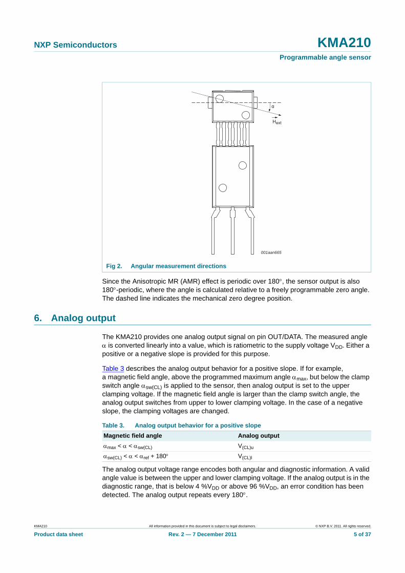
5.1 Angular measurement directions
The differential signals of the MR sensor bridges depend only on the direction of the external magnetic field strength Hext, which is applied parallel to the plane of the sensor. In order to obtain a correct output signal, the minimum saturation field strength has to be exceeded.
KMA210 All information provided in this document is subject to legal disclaimers. © NXP B.V. 2011. All rights reserved.
Product data sheet Rev. 2 — 7 December 2011 4 of 37
NXP Semiconductors KMA210Programmable angle sensor
Since the Anisotropic MR (AMR) effect is periodic over 180, the sensor output is also 180-periodic, where the angle is calculated relative to a freely programmable zero angle. The dashed line indicates the mechanical zero degree position.
6. Analog output
The KMA210 provides one analog output signal on pin OUT/DATA. The measured angle is converted linearly into a value, which is ratiometric to the supply voltage VDD. Either a positive or a negative slope is provided for this purpose.
Table 3 describes the analog output behavior for a positive slope. If for example, a magnetic field angle, above the programmed maximum angle max, but below the clamp switch angle sw(CL) is applied to the sensor, then analog output is set to the upper clamping voltage. If the magnetic field angle is larger than the clamp switch angle, the analog output switches from upper to lower clamping voltage. In the case of a negative slope, the clamping voltages are changed.
The analog output voltage range encodes both angular and diagnostic information. A valid angle value is between the upper and lower clamping voltage. If the analog output is in the diagnostic range, that is below 4 %VDD or above 96 %VDD, an error condition has been detected. The analog output repeats every 180.
Fig 2. Angular measurement directions
001aan665
Hext
α
Table 3. Analog output behavior for a positive slope
Magnetic field angle Analog output
max < < sw(CL) V(CL)u
sw(CL) < < ref + 180 V(CL)l
KMA210 All information provided in this document is subject to legal disclaimers. © NXP B.V. 2011. All rights reserved.
Product data sheet Rev. 2 — 7 December 2011 5 of 37

NXP Semiconductors KMA210Programmable angle sensor
7. Diagnostic features
The KMA210 provides several diagnostic features:
7.1 CRC and EDC supervision
The KMA210 includes a supervision of the programmed data. At power-on, a CRC of the non-volatile memory is performed. Furthermore the memory is protected against bit errors. Every 16-bit data word is saved internally as a 22-bit word for this purpose. The protection logic corrects any single-bit error in a data word, while the sensor continues in normal operation mode. Double-bit errors per word will be detected and switches the device into diagnostic mode.
7.2 Magnet-loss detection
If the applied magnetic field strength is not sufficient, the KMA210 can raise a diagnostic condition. In order to enter the diagnostic mode, due to magnet-loss, the detection has to be enabled first. The device can be programmed into active diagnostic mode, where the output is driven below 4 %VDD or above 96 %VDD.
7.3 Power-loss detection
The power-loss detection circuit enables the detection of an interrupted supply or ground line of the mixed signal IC in normal operation mode up to the maximum operating supply voltage. In the case of a power-loss condition, two internal switches in the sensor are closed, connecting the pin of the analog output to the supply voltage and the ground pins.
max = ref + rng
Fig 3. Characteristic of the analog output
001aag811
αrng
0 αref αmaxαsw(CL)
αref + 180°
α (deg)180
VO(%VDD)
V(CL)u
V(CL)I
KMA210 All information provided in this document is subject to legal disclaimers. © NXP B.V. 2011. All rights reserved.
Product data sheet Rev. 2 — 7 December 2011 6 of 37

NXP Semiconductors KMA210Programmable angle sensor
Table 4 describes the power-loss behavior and gives the resulting output voltage depending on the interrupted supply or ground line and the load resistance.
7.4 Broken bond wire detection
The broken bond wire detection circuit enables the detection of an interrupted supply or ground line of the MR sensor bridge. In the case of a broken bond wire the device goes into diagnostic mode and a status bit is set.
7.5 Low supply voltage detection and overvoltage protection
If the supply voltage is below the switch-off threshold voltage, a status bit is set and the device goes into diagnostic mode. If the supply voltage is above the overvoltage switch-on threshold voltage, the device enters diagnostic mode. Table 5 describes the system behavior depending on the voltage range of the supply voltage.
Fig 4. Equivalent output circuit in case of a power-loss condition
Table 4. Power-loss behavior
Load resistance Interrupted supply line Interrupted ground line
RL(ext) > 5 k VO 4 %VDD VO 96 %VDD
008aaa259
ZO(pl)
ZO(pl)
OUT/DATA
GND
VDDKMA210
Table 5. System behavior
Supply voltage State Description
0 V to 1.8 V start-up power The output buffer drives an active LOW or is powered down, but the switches of the power-loss detection circuit are not fully opened and set the output to a level between ground and half the supply voltage.
1.8 V to VPOR power-on reset
The power-loss charge pump is fully operational and turns the switches of the detection circuit off. The output buffer drives an active LOW and sets the output to the lower diagnostic level. During the reset phase all circuits are in reset and/or Power-down mode.
VPOR to Vth(on) or Vth(off)
initialization The digital core and the oscillator are active. After reset the content of the non-volatile memory is copied into the shadow registers. The output buffer drives an active LOW and sets the output to the lower diagnostic level.
Vth(on) or Vth(off) to minimum VDD
functional operation
All analog circuits are active and the measured angle is available at the analog output. Not all parameters are within the specified limits.
KMA210 All information provided in this document is subject to legal disclaimers. © NXP B.V. 2011. All rights reserved.
Product data sheet Rev. 2 — 7 December 2011 7 of 37

NXP Semiconductors KMA210Programmable angle sensor
Table 6 describes the diagnostic behavior and the resulting output voltage depending on the error case. Furthermore the duration and termination condition to enter and leave the diagnostic mode are given, respectively.
[1] Status bit stays set in command register until power-on reset.
[2] Depending on the diagnostic level setting.
8. Limiting values
[1] Overvoltage on analog output and supply within the specified operating voltage range.
Minimum VDD to maximum VDD
normal operation
All analog circuits are active and the measured angle is available at the analog output. All parameters are within the specified limits.
Maximum VDD to Vth(ov)
functional operation
All analog circuits are active and the measured angle is available at the analog output. Not all parameters are within the specified limits.
Vth(ov) to 16 V overvoltage The digital core and the oscillator are active but all other circuits are in Power-down mode. The output is set to the lower diagnostic level.
Table 6. Diagnostic behavior
Diagnostic condition Duration Analog output Termination condition
Low voltage 1 s < t < 10 s 4 %VDD functional or normal operation
Overvoltage 1 s < t < 10 s 4 %VDD functional or normal operation
Checksum error n/a 4 %VDD or 96 %VDD[2] power-on reset[1]
Double-bit error n/a 4 %VDD or 96 %VDD[2] power-on reset[1]
Magnet-loss 0.5 ms < t < 6 ms 4 %VDD or 96 %VDD[2] magnet present[1]
Power-loss 2 ms 4 %VDD or 96 %VDD[2] power-on reset
Broken bond wire 0.2 ms < t < 1 ms 4 %VDD or 96 %VDD[2] power-on reset[1]
Table 5. System behavior …continued
Supply voltage State Description
Table 7. Limiting valuesIn accordance with the Absolute Maximum Rating System (IEC 60134).
Symbol Parameter Conditions Min Max Unit
VDD supply voltage 0.3 +16 V
VO output voltage 0.3 +16 V
VO(ov) overvoltage output voltage Tamb < 140 C at t < 1 h
[1] Vth(ov) 16 V
Ir reverse current Tamb < 70 C - 150 mA
Tamb ambient temperature 40 +160 C
Tamb(pr) programming ambient temperature 10 70 C
Tstg storage temperature 40 +125 C
Non-volatile memory
tret(D) data retention time Tamb = 50 C 17 - year
Nendu(W_ER) write or erase endurance Tamb(pr) = 70 C 100 - cycle
KMA210 All information provided in this document is subject to legal disclaimers. © NXP B.V. 2011. All rights reserved.
Product data sheet Rev. 2 — 7 December 2011 8 of 37

NXP Semiconductors KMA210Programmable angle sensor
9. Recommended operating conditions
[1] Normal operation mode.
[2] Between ground and analog output.
[3] Command mode.
[4] Power-loss detection is only possible with a load resistance within the specified range connected to the supply or ground line.
10. Thermal characteristics
11. Characteristics
[1] Normal operation and diagnostic mode excluding overvoltage and undervoltage within the specified operating supply voltage range.
[2] Without load current at the analog output.
[3] Normal operation and diagnostic mode over full voltage range up to limiting supply voltage at steady state.
[4] With minimum load resistance at the analog output.
[5] Diagnostic mode for a supply voltage above the overvoltage threshold voltage up to the limiting supply voltage.
Table 8. Operating conditionsIn a homogenous magnetic field.
Symbol Parameter Conditions Min Typ Max Unit
VDD supply voltage [1] 4.5 5.0 5.5 V
Tamb ambient temperature 40 - +160 C
Tamb(pr) programming ambient temperature 10 - 70 C
CL(ext) external load capacitance [1][2] 0 - 22 nF[2][3] 0 - 6.8 nF
RL(ext) external load resistance [4] 5 - k
Hext external magnetic field strength 35 - - kA/m
Table 9. Thermal characteristics
Symbol Parameter Conditions Typ Unit
Rth(j-a) thermal resistance from junction to ambient
145 K/W
Table 10. Supply currentCharacteristics are valid for the operating conditions, as specified in Section 9.
Symbol Parameter Conditions Min Typ Max Unit
IDD supply current [1][2] 5 - 10.5 mA[3][4] - - 13 mA
Ioff(ov) overvoltage switch-off current [5] - - 6 mA
KMA210 All information provided in this document is subject to legal disclaimers. © NXP B.V. 2011. All rights reserved.
Product data sheet Rev. 2 — 7 December 2011 9 of 37
NXP Semiconductors KMA210Programmable angle sensor
Table 11. Power-on resetCharacteristics are valid for the operating conditions, as specified in Section 9.
Symbol Parameter Conditions Min Typ Max Unit
Vth(on) switch-on threshold voltage
analog output switches on, if VDD > Vth(on)
- 4.30 4.45 V
Vth(off) switch-off threshold voltage
analog output switches off, if VDD < Vth(off)
3.90 4.10 - V
Vhys hysteresis voltage Vhys = Vth(on) Vth(off) 0.1 0.2 - V
VPOR power-on reset voltage IC is initialized - 3.3 3.6 V
Vth(ov) overvoltage threshold voltage
analog output switches off, if VDD > Vth(ov)
6.5 7.5 8.0 V
Vhys(ov) overvoltage hysteresis voltage
0.1 0.3 - V
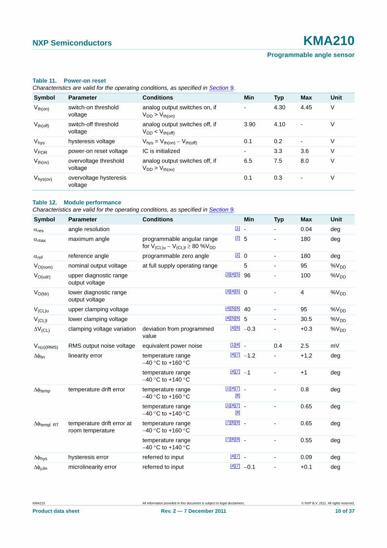
Table 12. Module performanceCharacteristics are valid for the operating conditions, as specified in Section 9.
Symbol Parameter Conditions Min Typ Max Unit
res angle resolution [1] - - 0.04 deg
max maximum angle programmable angular range for V(CL)u V(CL)l 80 %VDD
[2] 5 - 180 deg
ref reference angle programmable zero angle [2] 0 - 180 deg
VO(nom) nominal output voltage at full supply operating range 5 - 95 %VDD
VO(udr) upper diagnostic range output voltage
[3][4][5] 96 - 100 %VDD
VO(ldr) lower diagnostic range output voltage
[3][4][5] 0 - 4 %VDD
V(CL)u upper clamping voltage [4][5][6] 40 - 95 %VDD
V(CL)l lower clamping voltage [4][5][6] 5 - 30.5 %VDD
V(CL) clamping voltage variation deviation from programmed value
[4][5] 0.3 - +0.3 %VDD
Vn(o)(RMS) RMS output noise voltage equivalent power noise [1][4] - 0.4 2.5 mV
lin linearity error temperature range 40 C to +160 C
[4][7] 1.2 - +1.2 deg
temperature range 40 C to +140 C
[4][7] 1 - +1 deg
temp temperature drift error temperature range 40 C to +160 C
[1][4][7]
[8]- - 0.8 deg
temperature range 40 C to +140 C
[1][4][7]
[8]- - 0.65 deg
tempRT temperature drift error at room temperature
temperature range 40 C to +160 C
[7][8][9] - - 0.65 deg
temperature range 40 C to +140 C
[7][8][9] - - 0.55 deg
hys hysteresis error referred to input [4][7] - - 0.09 deg
lin microlinearity error referred to input [4][7] 0.1 - +0.1 deg
KMA210 All information provided in this document is subject to legal disclaimers. © NXP B.V. 2011. All rights reserved.
Product data sheet Rev. 2 — 7 December 2011 10 of 37

NXP Semiconductors KMA210Programmable angle sensor
[1] At a nominal output voltage between 5 %VDD and 95 %VDD and a maximum angle of max = 180.
[2] In steps of resolution < 0.022.
[3] Activation is dependent on the programmed diagnostic mode.
[4] At a low-pass filtered analog output with a cut-off frequency of 0.7 kHz.
[5] Settling to these values is limited by 0.7 kHz low-pass filtering of analog output.
[6] In steps of 0.02 %VDD.
[7] Definition of errors is given in Section 12.
[8] Based on a 3 standard deviation.
[9] Room temperature is given for an ambient temperature of 25 C.
[10] Graph of angular error is shown in Figure 5.
ang angular error temperature range 40 C to +160 C
[4][7] [10]
1.35 - +1.35 deg
temperature range 40 C to +140 C
[4][7] [10]
1.1 - +1.1 deg
mang slope of angular error [4][7] [10]
- - 0.04 deg/deg
ZO(pl) power-loss output impedance
impedance to remaining supply line in case of lost supply voltage or lost ground
- - 210
Table 12. Module performance …continuedCharacteristics are valid for the operating conditions, as specified in Section 9.
Symbol Parameter Conditions Min Typ Max Unit
(1) 40 C to +160 C
(2) 40 C to +140 C
Fig 5. Envelope curve for the magnitude of angular error
001aal765
1.401.35
|Δφang|(deg)
1.10
0.75
0.65
0−16 −12.25 −1 0 1 12.25
α1 − α0 (deg)16 20−20
(1)(2)
KMA210 All information provided in this document is subject to legal disclaimers. © NXP B.V. 2011. All rights reserved.
Product data sheet Rev. 2 — 7 December 2011 11 of 37
NXP Semiconductors KMA210Programmable angle sensor
[1] Measured at 1 MHz.
Table 13. DynamicsCharacteristics are valid for the operating conditions, as specified in Section 9.
Symbol Parameter Conditions Min Typ Max Unit
ton turn-on time until first valid result - - 5 ms
fupd update frequency 2.4 3.125 - kHz
ts settling time after an ideal mechanical angle step of 45, until 90 % of the final value is reached
- - 1.8 ms
tcmd(ent) enter command mode time after power on 20 - 30 ms
trec(ov) overvoltage recovery time after overvoltage - - 4 ms
Table 14. Digital interfaceCharacteristics are valid for the operating conditions, as specified in Section 9.
Symbol Parameter Conditions Min Typ Max Unit
VIH HIGH-level input voltage 80 - - %VDD
VIL LOW-level input voltage - - 20 %VDD
VOH HIGH-level output voltage IO = 2 mA 80 - - %VDD
VOL LOW-level output voltage IO = 2 mA - - 20 %VDD
Iod overdrive current absolute value for overdriving the output buffer
- - 20 mA
tstart start time LOW level before rising edge 5 - - s
tstop stop time HIGH level before falling edge 5 - - s
Tbit bit period minimum period may be limited by the load capacitance
10 - 100 s
Tbit bit period deviation deviation between received clock and sent clock
0.8Tbit 1Tbit 1.2Tbit s
tw0 pulse width 0 0.175Tbit 0.25Tbit 0.375Tbit s
tw1 pulse width 1 0.625Tbit 0.75Tbit 0.825Tbit s
tto time-out time communication reset guaranteed after maximum tto
- - 220 s
ttko(slv) slave takeover time duration of LOW level for slave takeover
1 - 5 s
ttko(mas) master takeover time duration of LOW level for master takeover
0Tbit - 0.5Tbit s
tprog programming time for a single memory address 20 - - ms
tcp charge pump time waiting time after enabling the non-volatile memory charge pump clock
1 - - ms
Table 15. Internal capacitancesCharacteristics are valid for the operating conditions, as specified in Section 9.
Symbol Parameter Conditions Min Typ Max Unit
Cblock blocking capacitance [1] 25 47 75 nF
CL load capacitance [1] 1.1 2.2 3.3 nF
KMA210 All information provided in this document is subject to legal disclaimers. © NXP B.V. 2011. All rights reserved.
Product data sheet Rev. 2 — 7 December 2011 12 of 37

NXP Semiconductors KMA210Programmable angle sensor
12. Definition of errors
12.1 General
Angular measurement errors by the KMA210 result from linearity errors, temperature drift errors and hysteresis errors. Figure 6 shows the output signal of an ideal sensor, where the measured angle meas corresponds ideally to the magnetic field angle . This curve will further be denoted as angle reference line ref() with a slope of 0.5 %VDD/degree.
The angular range is set to max = 180 and the clamping voltages are programmed to V(CL)l = 5 %VDD and V(CL)u = 95 %VDD for a valid definition of errors.
12.2 Hysteresis error
The hysteresis error hys is defined as the maximum difference between the angles, given by the device output when performing a positive (clockwise) rotation and negative (counter clockwise) rotation over an angular range of 180, measured at a constant temperature.
Equation 1 gives the mathematical description for the hysteresis value hys:
(1)
Fig 6. Definition of the reference line
001aag812
180 α (deg)
φmeas(deg)
φref(α)
Fig 7. Definition of the hysteresis error
001aag813
180 α (deg)
φmeas(deg)
Δφhys
hys ( ) meas 180( ) meas 0( )–=
KMA210 All information provided in this document is subject to legal disclaimers. © NXP B.V. 2011. All rights reserved.
Product data sheet Rev. 2 — 7 December 2011 13 of 37

NXP Semiconductors KMA210Programmable angle sensor
12.3 Linearity error
The KMA210 output signal deviation from a best straight line BSL, with the same slope as the reference line, is defined as linearity error. The magnetic field angle is varied at fixed temperatures for measurement of this linearity error. The output signal deviation from the best straight line at the given temperature is the linearity error lin. It is a function of the magnetic field angle and the temperature of the device Tamb.
12.4 Microlinearity error
The microlinearity error lin is the device output deviation from 1, if the magnetic field angle is changed by = 1.
12.5 Temperature drift error
The temperature drift temp is defined as the envelope over the deviation of the angle versus the temperature range. It is considered as the pure thermal effect.
Fig 8. Definition of the linearity error
001aag814
180 α (deg)
φmeas(deg)
Δφlin(α, Tamb)φref(α)
φBSL(α, Tamb)
Fig 9. Definition of the microlinearity error
001aag815
α (deg)
φmeas(deg)
Δφmeas = 1° + Δφμlin(α)
φref(α)
Δα = 1°
KMA210 All information provided in this document is subject to legal disclaimers. © NXP B.V. 2011. All rights reserved.
Product data sheet Rev. 2 — 7 December 2011 14 of 37

NXP Semiconductors KMA210Programmable angle sensor
Equation 2 gives the mathematical description for temperature drift value temp:
(2)
with:
Tx: temperature for maximum meas at angle
Ty: temperature for minimum meas at angle
The deviation from the value at room temperature tempRT describes the temperature drift of the angle, compared to the value, which the sensor provides at room temperature:
(3)
with:
TRT: room temperature (25 C)
12.6 Angular error
The angular error ang is the error of angle difference measured by the sensor, if the mechanical angle deviates from 0 to 1. Here 0 and 1 are arbitrary angles within the angular range. The angle measurement at 0 is the initially programmed reference angle, programmed by the customer at room temperature and zero hour upon production. The angle measurement at 1 is made at any temperature within the ambient temperature range:
(4)
with:
0, 1: arbitrary mechanical angles within the angular range
meas(0, TRT): programmed angle at 0, TRT = 25 C and zero hour upon production
meas(1, Tamb): angle measured by the sensor at 1 and any temperature within Tamb
This error comprises non-linearity and temperature drift related to the room temperature.
Fig 10. Definition of the temperature drift error
001aag816
180 α (deg)
φmeas(deg)
Δφtemp
Ty
Tx
temp ( ) meas Tx,( ) meas Ty,( )–=
temp RT Tamb,( ) meas Tamb,( ) meas TRT,( )–=
ang meas 1 Tamb,( ) meas 0 TRT,( )– 1 0– –=
KMA210 All information provided in this document is subject to legal disclaimers. © NXP B.V. 2011. All rights reserved.
Product data sheet Rev. 2 — 7 December 2011 15 of 37
NXP Semiconductors KMA210Programmable angle sensor
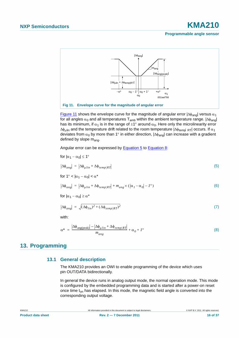
Figure 11 shows the envelope curve for the magnitude of angular error |ang| versus 1 for all angles 0 and all temperatures Tamb within the ambient temperature range. |ang| has its minimum, if 1 is in the range of 1 around 0. Here only the microlinearity error lin and the temperature drift related to the room temperature |tempRT| occurs. If 1 deviates from 0 by more than 1 in either direction, |ang| can increase with a gradient defined by slope mang.
Angular error can be expressed by Equation 5 to Equation 8:
for |1 0| 1
(5)
for 1 < |1 0| < *
(6)
for |1 0| *
(7)
with:
(8)
13. Programming
13.1 General description
The KMA210 provides an OWI to enable programming of the device which uses pin OUT/DATA bidirectionally.
In general the device runs in analog output mode, the normal operation mode. This mode is configured by the embedded programming data and is started after a power-on reset once time ton has elapsed. In this mode, the magnetic field angle is converted into the corresponding output voltage.
Fig 11. Envelope curve for the magnitude of angular error
001aal766
|Δφμlin + Δφtemp|RT|
−α* α0 − 1°α0
|Δφang|
α0 + 1° +α*
mang
|Δφang(peak)|
α1
ang lin temp RT+=
ang lin temp RT+ mang 1 0– 1– +=
ang lin 2 temp RT 2+=
ang(peak) lin temp RT+–
mang----------------------------------------------------------------------------------- 0 1+ +=
KMA210 All information provided in this document is subject to legal disclaimers. © NXP B.V. 2011. All rights reserved.
Product data sheet Rev. 2 — 7 December 2011 16 of 37
NXP Semiconductors KMA210Programmable angle sensor
Command mode has to be entered to enable programming. In this mode, the customer can adjust all required parameters (for example zero angle and angular range) to meet the application requirements. After enabling the internal charge pump and waiting for tcp the data is stored in the non-volatile memory. After changing the contents of the memory, the checksum must be recalculated and written (see Section 13.4).
In order to enter the command mode, a specific command sequence must be sent after a power-on reset and during the time slot tcmd(ent). The external source used to send the command sequence must overdrive the output buffer of the KMA210. In doing so it provides current Iod.
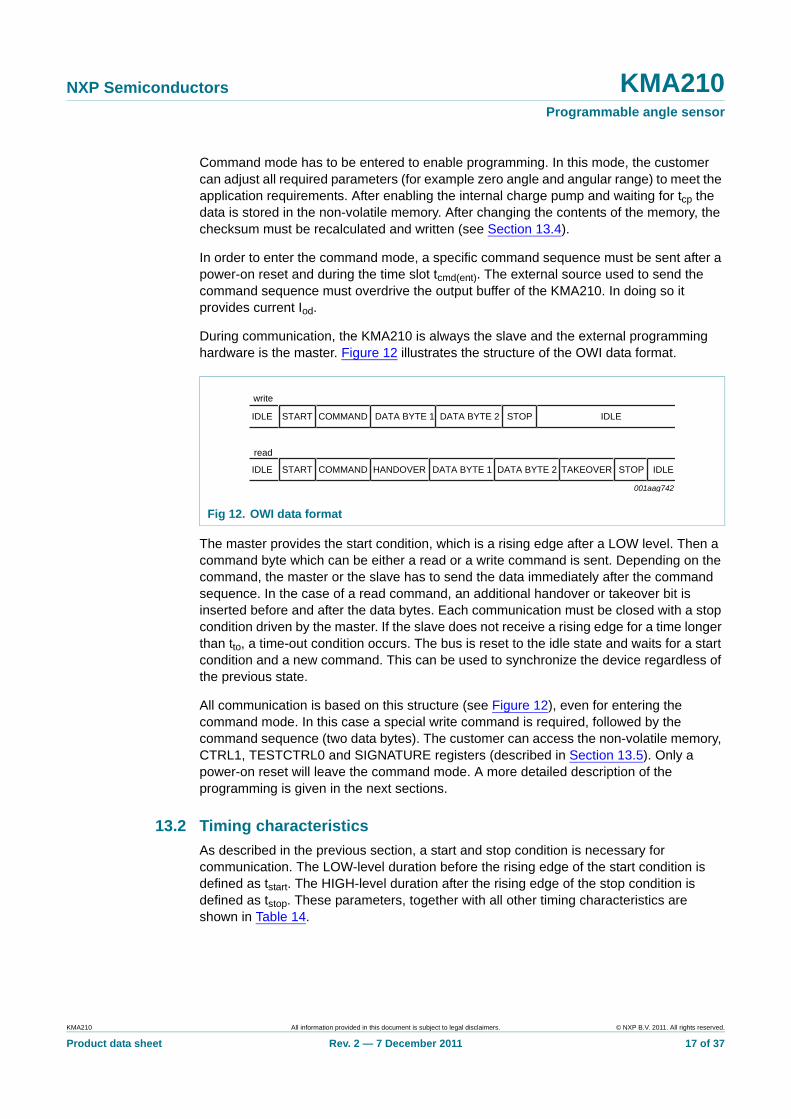
During communication, the KMA210 is always the slave and the external programming hardware is the master. Figure 12 illustrates the structure of the OWI data format.
The master provides the start condition, which is a rising edge after a LOW level. Then a command byte which can be either a read or a write command is sent. Depending on the command, the master or the slave has to send the data immediately after the command sequence. In the case of a read command, an additional handover or takeover bit is inserted before and after the data bytes. Each communication must be closed with a stop condition driven by the master. If the slave does not receive a rising edge for a time longer than tto, a time-out condition occurs. The bus is reset to the idle state and waits for a start condition and a new command. This can be used to synchronize the device regardless of the previous state.
All communication is based on this structure (see Figure 12), even for entering the command mode. In this case a special write command is required, followed by the command sequence (two data bytes). The customer can access the non-volatile memory, CTRL1, TESTCTRL0 and SIGNATURE registers (described in Section 13.5). Only a power-on reset will leave the command mode. A more detailed description of the programming is given in the next sections.
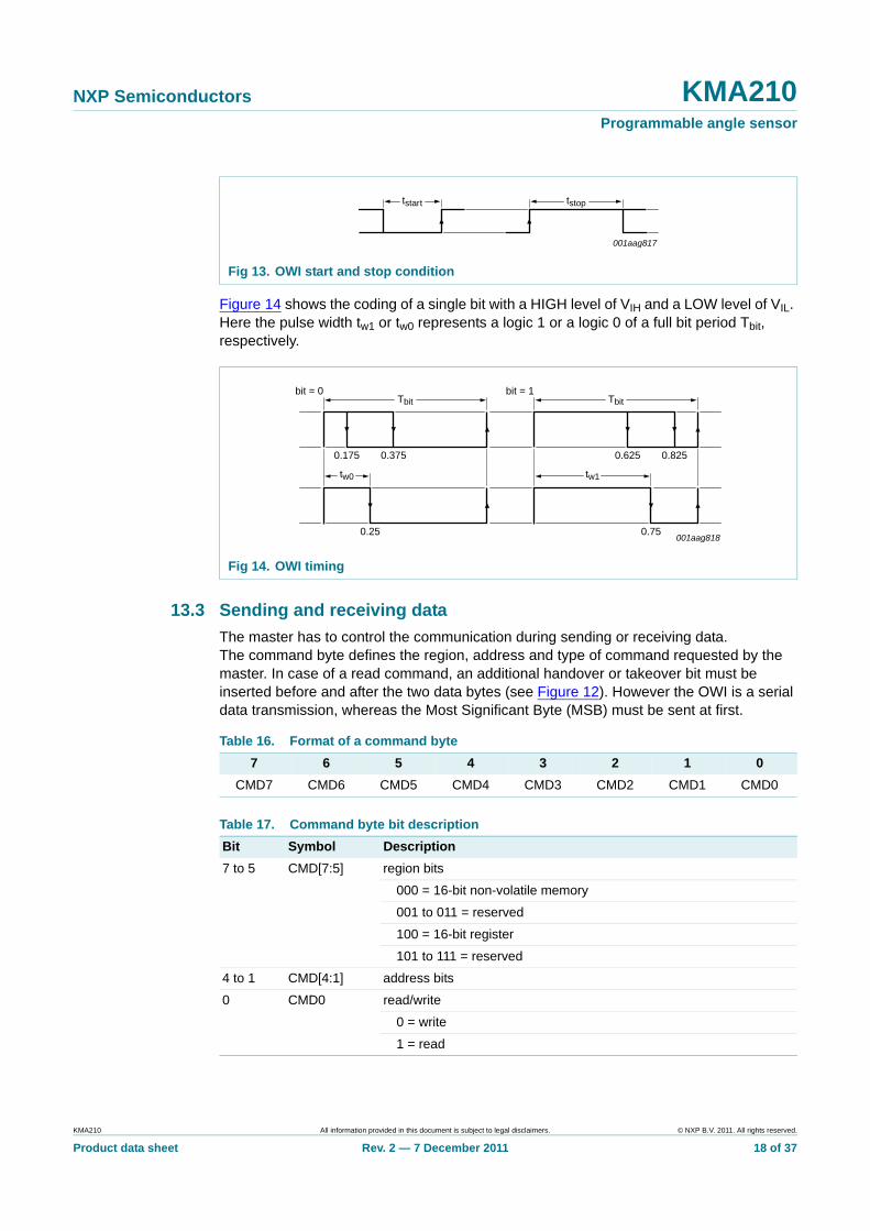
13.2 Timing characteristics
As described in the previous section, a start and stop condition is necessary for communication. The LOW-level duration before the rising edge of the start condition is defined as tstart. The HIGH-level duration after the rising edge of the stop condition is defined as tstop. These parameters, together with all other timing characteristics are shown in Table 14.
Fig 12. OWI data format
001aag742
write
IDLE IDLESTART STOPCOMMAND DATA BYTE 1 DATA BYTE 2
IDLE START COMMAND HANDOVER TAKEOVER STOP IDLEDATA BYTE 1 DATA BYTE 2
read
KMA210 All information provided in this document is subject to legal disclaimers. © NXP B.V. 2011. All rights reserved.
Product data sheet Rev. 2 — 7 December 2011 17 of 37
NXP Semiconductors KMA210Programmable angle sensor
Figure 14 shows the coding of a single bit with a HIGH level of VIH and a LOW level of VIL. Here the pulse width tw1 or tw0 represents a logic 1 or a logic 0 of a full bit period Tbit, respectively.
13.3 Sending and receiving data
The master has to control the communication during sending or receiving data. The command byte defines the region, address and type of command requested by the master. In case of a read command, an additional handover or takeover bit must be inserted before and after the two data bytes (see Figure 12). However the OWI is a serial data transmission, whereas the Most Significant Byte (MSB) must be sent at first.
Fig 13. OWI start and stop condition
Fig 14. OWI timing
001aag817
tstart tstop
001aag818
0.175
bit = 0 bit = 1
0.25
0.375
Tbit
tw0 tw1
0.625
0.75
0.825
Tbit
Table 16. Format of a command byte
7 6 5 4 3 2 1 0
CMD7 CMD6 CMD5 CMD4 CMD3 CMD2 CMD1 CMD0
Table 17. Command byte bit description
Bit Symbol Description
7 to 5 CMD[7:5] region bits
000 = 16-bit non-volatile memory
001 to 011 = reserved
100 = 16-bit register
101 to 111 = reserved
4 to 1 CMD[4:1] address bits
0 CMD0 read/write
0 = write
1 = read
KMA210 All information provided in this document is subject to legal disclaimers. © NXP B.V. 2011. All rights reserved.
Product data sheet Rev. 2 — 7 December 2011 18 of 37
NXP Semiconductors KMA210Programmable angle sensor
A more detailed description of all customer accessible registers is given in Section 13.5. Both default value and the complete command including the address and write or read request are also listed.
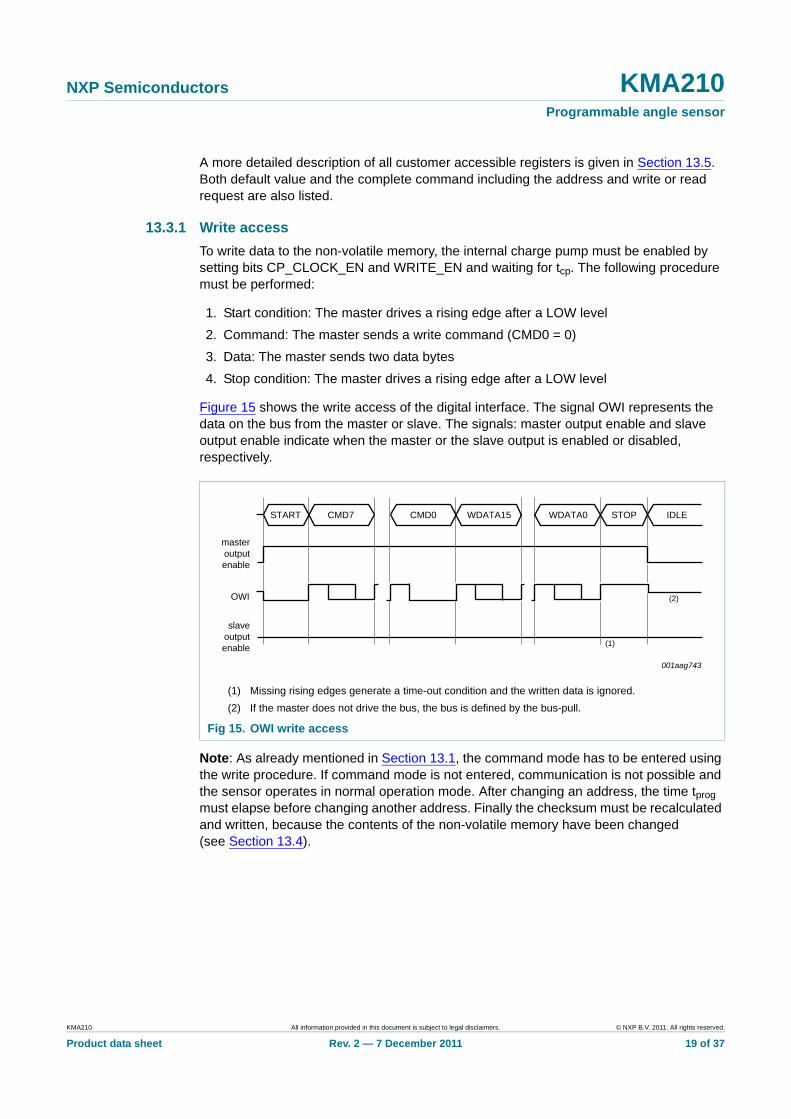
13.3.1 Write access
To write data to the non-volatile memory, the internal charge pump must be enabled by setting bits CP_CLOCK_EN and WRITE_EN and waiting for tcp. The following procedure must be performed:
1. Start condition: The master drives a rising edge after a LOW level
2. Command: The master sends a write command (CMD0 = 0)
3. Data: The master sends two data bytes
4. Stop condition: The master drives a rising edge after a LOW level
Figure 15 shows the write access of the digital interface. The signal OWI represents the data on the bus from the master or slave. The signals: master output enable and slave output enable indicate when the master or the slave output is enabled or disabled, respectively.
Note: As already mentioned in Section 13.1, the command mode has to be entered using the write procedure. If command mode is not entered, communication is not possible and the sensor operates in normal operation mode. After changing an address, the time tprog must elapse before changing another address. Finally the checksum must be recalculated and written, because the contents of the non-volatile memory have been changed (see Section 13.4).
(1) Missing rising edges generate a time-out condition and the written data is ignored.
(2) If the master does not drive the bus, the bus is defined by the bus-pull.
Fig 15. OWI write access
001aag743
masteroutputenable
slaveoutputenable
START CMD7 CMD0 STOP
(1)
(2)
IDLEWDATA15 WDATA0
OWI
KMA210 All information provided in this document is subject to legal disclaimers. © NXP B.V. 2011. All rights reserved.
Product data sheet Rev. 2 — 7 December 2011 19 of 37
NXP Semiconductors KMA210Programmable angle sensor
13.3.2 Read access
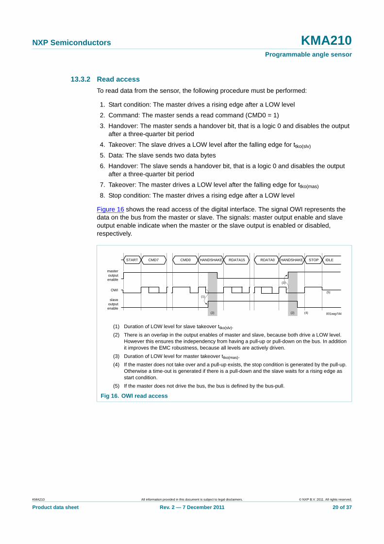
To read data from the sensor, the following procedure must be performed:
1. Start condition: The master drives a rising edge after a LOW level
2. Command: The master sends a read command (CMD0 = 1)
3. Handover: The master sends a handover bit, that is a logic 0 and disables the output after a three-quarter bit period
4. Takeover: The slave drives a LOW level after the falling edge for ttko(slv)
5. Data: The slave sends two data bytes
6. Handover: The slave sends a handover bit, that is a logic 0 and disables the output after a three-quarter bit period
7. Takeover: The master drives a LOW level after the falling edge for ttko(mas)
8. Stop condition: The master drives a rising edge after a LOW level
Figure 16 shows the read access of the digital interface. The signal OWI represents the data on the bus from the master or slave. The signals: master output enable and slave output enable indicate when the master or the slave output is enabled or disabled, respectively.
(1) Duration of LOW level for slave takeover ttko(slv).
(2) There is an overlap in the output enables of master and slave, because both drive a LOW level. However this ensures the independency from having a pull-up or pull-down on the bus. In addition it improves the EMC robustness, because all levels are actively driven.
(3) Duration of LOW level for master takeover ttko(mas).
(4) If the master does not take over and a pull-up exists, the stop condition is generated by the pull-up. Otherwise a time-out is generated if there is a pull-down and the slave waits for a rising edge as start condition.
(5) If the master does not drive the bus, the bus is defined by the bus-pull.
Fig 16. OWI read access
001aag744
masteroutputenable
slaveoutputenable
START CMD7 CMD0 RDATA0
(1)
(2) (2) (4)
(5)
(3)
HANDSHAKE HANDSHAKERDATA15 IDLESTOP
OWI
KMA210 All information provided in this document is subject to legal disclaimers. © NXP B.V. 2011. All rights reserved.
Product data sheet Rev. 2 — 7 December 2011 20 of 37
NXP Semiconductors KMA210Programmable angle sensor
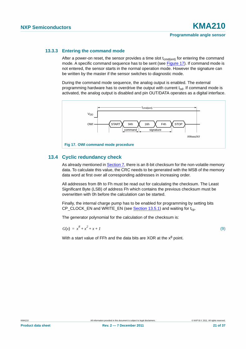
13.3.3 Entering the command mode
After a power-on reset, the sensor provides a time slot tcmd(ent) for entering the command mode. A specific command sequence has to be sent (see Figure 17). If command mode is not entered, the sensor starts in the normal operation mode. However the signature can be written by the master if the sensor switches to diagnostic mode.
During the command mode sequence, the analog output is enabled. The external programming hardware has to overdrive the output with current Iod. If command mode is activated, the analog output is disabled and pin OUT/DATA operates as a digital interface.
13.4 Cyclic redundancy check
As already mentioned in Section 7, there is an 8-bit checksum for the non-volatile memory data. To calculate this value, the CRC needs to be generated with the MSB of the memory data word at first over all corresponding addresses in increasing order.
All addresses from 8h to Fh must be read out for calculating the checksum. The Least Significant Byte (LSB) of address Fh which contains the previous checksum must be overwritten with 0h before the calculation can be started.
Finally, the internal charge pump has to be enabled for programming by setting bits CP_CLOCK_EN and WRITE_EN (see Section 13.5.1) and waiting for tcp.
The generator polynomial for the calculation of the checksum is:
(9)
With a start value of FFh and the data bits are XOR at the x8 point.
Fig 17. OWI command mode procedure
008aaa263
tcmd(ent)
signaturecommand
STARTOWI
VDD
94h 16h F4h STOP
G x( ) x8
x2
x 1+ + +=
KMA210 All information provided in this document is subject to legal disclaimers. © NXP B.V. 2011. All rights reserved.
Product data sheet Rev. 2 — 7 December 2011 21 of 37

NXP Semiconductors KMA210Programmable angle sensor
13.4.1 Software example in C
1 #include <stdio.h.>23 // calc_crc accepts unsigned 16-bit data in data4 int calc_crc(int crc, unsigned int data)5 {6 const int gpoly = 0x107; // generator polynomial7 int i; //index variable8 for (i = 15; i >= 0; i--)9 {10 crc <<= 1; //shift left11 crc = (int) ((data & (1u<<i))>>i);12 // XOR of with generator polynomial when MSB(9) = HIGH13 if (crc & 0x100) crc ^= gpoly;14 }15 return crc;16 }17 int main(void)18 {19 int crc, crc_res, i;20 // 8 LSB are CRC field filled with 021 unsigned int data_seq[] = {0x0000, 0xFFC1, 0x0400, 0x0100,22 0x1300, 0x0000, 0x0000, 0x0000};23 // calculate checksum over all data24 crc = 0xFF; // start value of crc register25 printf(“Address\tValue\n”);26 for (i = 0; i <= 7; i++)27 {28 printf(“0x%1X\t0x%04X\n”, i, data_seq[i]);29 crc = calc_crc(crc, data_seq[i]);30 }31 crc_res = crc; // crc_res = 0xA932 printf(“\nChecksum\n0x%02X\n”, crc_res);33 // check procedure for above data sequence34 crc = 0xFF;35 for (i = 0; i <= 6; i++)36 crc = calc_crc(crc, data_seq[i]);37 // last word gets crc inserted38 crc = calc_crc(crc, data_seq[i] crc_res);39 printf(“\nCheck procedure for data sequence: must be 0x00 is 0x%02X.\n”,crc);40 return 1;41 }
The checksum of this data sequence is A9h.
KMA210 All information provided in this document is subject to legal disclaimers. © NXP B.V. 2011. All rights reserved.
Product data sheet Rev. 2 — 7 December 2011 22 of 37

NXP Semiconductors KMA210Programmable angle sensor
13.5 Registers
13.5.1 Command registers
To enter the command mode, the signature given in Table 18 must be written into the specific register using the OWI. This must be done as described in Section 13.3.3, with a write command, followed by the signature, but after a power-on reset and not later than tcmd(ent).
Table 18. Command registers
Command write/read
Register Bit Access Field Description
82h/83h CTRL1 15 R IN_DIAG_MODE shows if there is a diagnostic condition present; this bit is not affected by the setting of register field FORCE_DIAG_OFF
14 W FORCE_DIAG_OFF force diagnostic mode off; default: 0b
13 - - reserved
12 R LOW_VOLTAGE_DET low voltage condition detected
11 R/W CP_CLOCK_EN charge pump clock enabled (must be set after setting write enable signal for writing to non-volatile memory); default: 0b
10 and 9 - - reserved
8 R ERR_CORRECT single-bit error of non-volatile memory has been detected and corrected; updated every memory readout; remains set until the diagnostic condition disappears and a power-on reset is done
7 R UNCORR_ERR double-bit error of non-volatile memory has been detected; updated every memory readout; remains set until the diagnostic condition disappears and a power-on reset is done
6 R MAGNET_LOSS_DET magnet-loss detected; bit remains set until the diagnostic condition disappears and a power-on reset is done; magnet-loss detection must be enabled for entering diagnostic mode
5 R BROKEN_BOND_DET broken bond wire detected; bit remains set until the diagnostic condition disappears and a power-on reset is done
4 R CRC_BAD checksum error detected; updated every start-up
3 to 0 - - reserved
94h/- SIGNATURE 15 to 0 W SIGNATURE write signature 16F4h within tcmd(ent) to enter command mode; see Section 13.3.3 for more details
96h/97h TESTCTRL0 15 to 12 - - reserved
11 W WRITE_EN write enable signal; must be set before writing to non-volatile memory; default: 0b
10 to 0 - - reserved
KMA210 All information provided in this document is subject to legal disclaimers. © NXP B.V. 2011. All rights reserved.
Product data sheet Rev. 2 — 7 December 2011 23 of 37

NXP Semiconductors KMA210Programmable angle sensor
13.5.2 Non-volatile memory registers
The device includes several internal registers which are used for customization and identification.
The initial signature allows read access to all areas but only write access to customer registers. Write accesses to reserved areas are ignored. Since these registers are implemented as non-volatile memory cells, writing to the registers needs a specific time tprog after each write access to complete.
As there is no check for the programming time, the user must make sure no other accesses to the non-volatile memory are made during the programming cycle. The non-volatile memory must not be addressed during the time tprog.
Note: Before data can be stored in the non-volatile memory, the internal charge pump has to be switched on for the programming duration by setting register CTRL1, bit 11 CP_CLOCK_EN and register TESTCTRL0, bit 11 WRITE_EN. Register addresses 8h to Fh have to be read out and consulted to calculate the checksum.
Table 19. Non-volatile memory registers
Address Command write/read
Register Bit Description Default MSB/LSB
0h -/01h reserved - addresses are reserved for calibration purposes [1]
1h -/03h
2h -/05h
3h -/07h
4h -/09h
5h -/0Bh
6h -/0Dh
7h -/0Fh
8h 10h/11h ZERO_ANGLE 15 to 0 mechanical zero degree position; see Table 20 00h/00h
9h 12h/13h ANG_RNG_MULT_MSB 15 to 6 CLAMP_SW_ANGLE; when the measured angle is bigger than CLAMP_SW_ANGLE the output switches to CLAMP_LO for a positive slope; see Table 25
FFh/C1h
5 to 0 ANG_RNG_MULT_MSB; most significant bits of the angular range multiplicator; see Table 23
Ah 14h/15h ANG_RNG_MULT_LSB 15 and 14 DIAGNOSTIC_LEVEL; diagnostic level behavior of the analog output; see Table 24
00b — active LOW (in lower diagnostic range) with driver strength of the analog output
01b — active HIGH (in upper diagnostic range) with driver strength of the analog output
10b — reserved
11b — reserved
04h/00h
13 SLOPE_DIR; slope of analog output
0b — rising (not inverted)
1b — falling (inverted)
12 to 0 ANG_RNG_MULT_LSB; least significant bits of the angular range multiplicator
KMA210 All information provided in this document is subject to legal disclaimers. © NXP B.V. 2011. All rights reserved.
Product data sheet Rev. 2 — 7 December 2011 24 of 37

NXP Semiconductors KMA210Programmable angle sensor
[1] Variable and individual for each device.
[2] Undefined; must be written as zero for default.
Mechanical angular range 0000h = 0 to FFFFh = 180 1 LSB.
Examples:
• Mechanical zero angle 0 = 0000h
• Mechanical zero angle 10 = 0E38h
• Mechanical zero angle 45 = 4000h
[1] Undefined; must be written as zero for default and may return any value when read.
Values 0 to 255 are reserved. It is not permitted to use such values.
Examples:
• 100 %VDD = 5120 (reserved)
• 10 %VDD = 512
• 5 %VDD = 256
Bh 16h/17h CLAMP_LO 15 0b — reserved 01h/00h
14 and 13 undefined[2]
12 to 0 lower clamping level; see Table 21
Ch 18h/19h CLAMP_HI 15 to 13 undefined[2] 13h/00h
12 to 0 upper clamping level; see Table 22
Dh 1Ah/1Bh ID_LO 15 to 0 lower 16 bits of identification code 00h/00h
Eh 1Ch/1Dh ID_HI 15 to 0 upper 16 bits of identification code 00h/00h
Fh 1Eh/1Fh CTRL_CUST 15 LOCK; irreversible write protection of non-volatile memory
1b — enabled
00h/[1]
14 to 8 MAGNET_LOSS; magnet-loss detection
00h — disabled
49h — enabled
7 to 0 CRC; checksum (see Section 13.4)
Table 19. Non-volatile memory registers …continued
Address Command write/read
Register Bit Description Default MSB/LSB
Table 20. ZERO_ANGLE - mechanical zero degree position (address 8h) bit allocationData format: unsigned fixed point; resolution: 216.
Bit 15 14 13 12 11 10 9 8 7 6 5 4 3 2 1 0
Value 21 22 23 24 25 26 27 28 29 210 211 212 213 214 215 216
Table 21. CLAMP_LO - lower clamping level (address Bh) bit allocationData format: unsigned integer (DAC values 256 to 4864); resolution: 20.
Bit 15 14 13 12 11 10 9 8 7 6 5 4 3 2 1 0
Value 0 U[1] U[1] 212 211 210 29 28 27 26 25 24 23 22 21 20
KMA210 All information provided in this document is subject to legal disclaimers. © NXP B.V. 2011. All rights reserved.
Product data sheet Rev. 2 — 7 December 2011 25 of 37

NXP Semiconductors KMA210Programmable angle sensor
[1] Undefined; must be written as zero for default and may return any value when read.
Values 4865 to 5120 are reserved. It is not permitted to use such values.
Examples:
• 100 %VDD = 5120 (reserved)
• 95 %VDD = 4864
• 90 %VDD = 4608
(10)
Examples:
•
•
[1] Variable; depending on the setting of diagnostic level and slope of analog output.
(11)
Mechanical angular range 0000h = 0 to 3FFh = 180 1 LSB.
(12)
If the magnetic field angle is larger than the CLAMP_SW_ANGLE, the output switches to CLAMP_LO for a positive slope. The value of CLAMP_SW_ANGLE can be calculated from other non-volatile memory constants but must be programmed.
Table 22. CLAMP_HI - upper clamping level (address Ch) bit allocationData format: unsigned integer (DAC values 256 to 4864); resolution: 20.
Bit 15 14 13 12 11 10 9 8 7 6 5 4 3 2 1 0
Value U[1] U[1] U[1] 212 211 210 29 28 27 26 25 24 23 22 21 20
Table 23. ANG_RNG_MULT_MSB - most significant bits of angular range multiplicator (address 9h) bit allocationData format: unsigned fixed point; resolution: 21.
Bit 15 14 13 12 11 10 9 8 7 6 5 4 3 2 1 0
Value CLAMP_SW_ANGLE 24 23 22 21 20 21
ANG_RNG_MULTCLAMP_HI CLAMP_LO–
8192-------------------------------------------------------------------- 180
ANGULAR_RANGE-----------------------------------------------------=
ANG_RNG_MULT4864 256–
8192--------------------------- 180
180----------- 0.5625= =
ANG_RNG_MULT4864 256–
8192--------------------------- 180
90----------- 1.125= =
Table 24. ANG_RNG_MULT_LSB - least significant bits of angular range multiplicator (address Ah) bit allocationData format: unsigned fixed point; resolution: 214.
Bit 15 14 13 12 11 10 9 8 7 6 5 4 3 2 1 0
Value V[1] V[1] 22 23 24 25 26 27 28 29 210 211 212 213 214
ANG_RNG_MULTCLAMP_HI CLAMP_LO–
8192-------------------------------------------------------------------- 180
ANGULAR_RANGE-----------------------------------------------------=
Table 25. CLAMP_SW_ANGLE - clamp switch angle (address 9h) bit allocationData format: unsigned fixed point; resolution: 210.
Bit 15 14 13 12 11 10 9 8 7 6 5 4 3 2 1 0
Value 21 22 23 24 25 26 27 28 29 210 ANG_RNG_MULT_MSB
CLAMP_SW_ANGLE12--- 1
CLAMP_HI CLAMP_LO–8192
--------------------------------------------------------------------- 1ANG_RNG_MULT-------------------------------------------------+
=
KMA210 All information provided in this document is subject to legal disclaimers. © NXP B.V. 2011. All rights reserved.
Product data sheet Rev. 2 — 7 December 2011 26 of 37
NXP Semiconductors KMA210Programmable angle sensor
14. Electromagnetic compatibility
EMC is verified in an independent and certified test laboratory.
14.1 Emission (CISPR 25)
Tests according to CISPR 25 were fulfilled.
14.1.1 Conducted radio disturbance
Test of the device according to CISPR 25, third edition (2008-03), Chapter 6.2.
Classification level: 5.
14.1.2 Radiated radio disturbance
Test of the device according to CISPR 25, third edition (2008-03), Chapter 6.4.
Classification level: 5 (without addition of 6 dB in FM band).
14.2 Radiated disturbances (ISO 11452-1 third edition (2005-02), ISO 11452-2, ISO 11452-4 and ISO 11452-5)
The common understanding of the requested function is that an effect is tolerated as described in Table 26 during the disturbance. The reachable values are setup dependent and may differ from the final application.
14.2.1 Absorber lined shielded enclosure
Tests according to ISO 11452-2, second edition (2004-11), were fulfilled.
Test level: 200 V/m; extended up to 10 GHz.
State: A.
14.2.2 Bulk-current injection
Tests according to ISO 11452-4, third edition (2005-04), were fulfilled.
Test level: 200 mA.
State: A.
14.2.3 Strip line
Tests according to ISO 11452-5, second edition (2002-04), were fulfilled.
Test level: 200 V/m; extended up to 1 GHz.
State: A.
Table 26. Failure condition for radiated disturbances
Parameter Comment Min Max Unit
Variation of output signal in analog output mode
value measured relative to the output at test start
- 0.9 %VDD
KMA210 All information provided in this document is subject to legal disclaimers. © NXP B.V. 2011. All rights reserved.
Product data sheet Rev. 2 — 7 December 2011 27 of 37

NXP Semiconductors KMA210Programmable angle sensor
14.2.4 Immunity against mobile phones
Tests according to ISO 11452-2, second edition (2004-11), were fulfilled.
State: A.
Definition of Global System for Mobile Communications (GSM) signal:
• Pulse modulation: per GSM specification (217 Hz; 12.5 % duty cycle)
• Modulation grade: 60 dB
• Sweep: linear 800 MHz to 3 GHz (duration 10 s at 890 MHz, 940 MHz and 1.8 GHz band)
• Antenna polarization: vertical, horizontal
• Field strength: 200 V/m during on-time [calibration in Continuous Wave (CW)]
In deviation of ISO 11452-2 a GSM signal (definition see above) instead of an AM signal was used.
14.3 Electrical transient transmission by capacitive coupling [ISO 7637-3, second edition (2007-07)]
The common understanding of the requested function is that an effect is tolerated as described in Table 27 during the disturbance.
Tests according to ISO 7637-3 were fulfilled.
Test level: IV (for 12 V electrical system).
Classification level: B for pulse Fast a, B for pulse Fast b.
Table 27. Failure condition for electrical transient transmission
Parameter Comment Min Max Unit
Variation of output signal in analog output mode
value measured relative to the output at test start
- 0.9 %VDD
KMA210 All information provided in this document is subject to legal disclaimers. © NXP B.V. 2011. All rights reserved.
Product data sheet Rev. 2 — 7 December 2011 28 of 37
NXP Semiconductors KMA210Programmable angle sensor
15. ElectroStatic Discharge (ESD)
15.1 Human body model (AEC-Q100-002)
The KMA210 must not be damaged at 8 kV, according to the human body model at 100 pF and 1.5 k. This protection is ensured at all external pins (OUT/DATA, VDD and GND).
Classification level: H3B.
Furthermore, all interconnects (pins between package head and package body) must not be damaged at 2 kV.
Classification level: H2.
15.2 Human metal model (ANSI/ESD SP5.6-2009)
The KMA210 must not be damaged at 8 kV, according to the human metal model at 150 pF and 330 inside the ESD gun. This test utilizes waveforms of the IEC 61000-4-2 standard on component level. The contact discharge will be applied in an unsupplied state at pins OUT/DATA and VDD referred to GND which is connected directly to the ground plane.
Test setup: A.
Test level: 5.
15.3 Machine model (AEC-Q100-003)
The KMA210 must not be damaged at 400 V, according to the machine model. This protection is ensured at all external pins (OUT/DATA, VDD and GND).
Classification level: M4.
Furthermore, all interconnects (pins between package head and package body) must not be damaged at 200 V.
Classification level: M3.
All pins have latch-up protection.
15.4 Charged-device model (AEC-Q100-011)
The KMA210 must not be damaged at 750 V, according to the charged-device model. This protection is ensured at all external pins (OUT/DATA, VDD and GND).
Classification level: C4.
Furthermore, all interconnects (pins between package head and package body) must not be damaged at 500 V.
Classification level: C3B.
KMA210 All information provided in this document is subject to legal disclaimers. © NXP B.V. 2011. All rights reserved.
Product data sheet Rev. 2 — 7 December 2011 29 of 37
NXP Semiconductors KMA210Programmable angle sensor
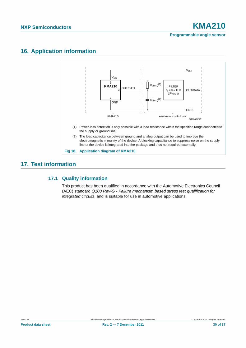
16. Application information
17. Test information
17.1 Quality information
This product has been qualified in accordance with the Automotive Electronics Council (AEC) standard Q100 Rev-G - Failure mechanism based stress test qualification for integrated circuits, and is suitable for use in automotive applications.
(1) Power-loss detection is only possible with a load resistance within the specified range connected to the supply or ground line.
(2) The load capacitance between ground and analog output can be used to improve the electromagnetic immunity of the device. A blocking capacitance to suppress noise on the supply line of the device is integrated into the package and thus not required externally.
Fig 18. Application diagram of KMA210
008aaa260
2
3
VDD
GND
OUT/DATA
KMA210 electronic control unit
VDD
GND
OUT/DATA
1RL(ext)(1)
CL(ext)(2)
KMA210 FILTERfg = 0.7 kHz
1st order
KMA210 All information provided in this document is subject to legal disclaimers. © NXP B.V. 2011. All rights reserved.
Product data sheet Rev. 2 — 7 December 2011 30 of 37
NXP Semiconductors KMA210Programmable angle sensor
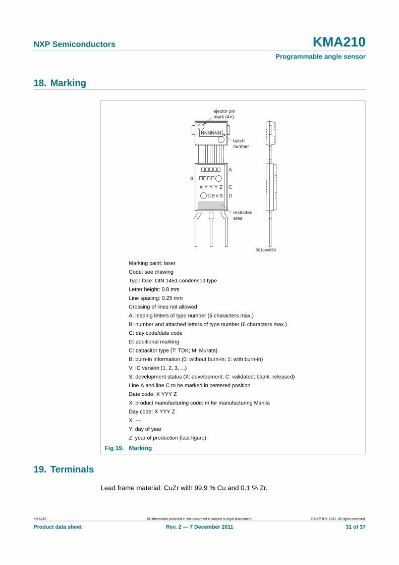
18. Marking
19. Terminals
Lead frame material: CuZr with 99.9 % Cu and 0.1 % Zr.
Marking paint: laser
Code: see drawing
Type face: DIN 1451 condensed type
Letter height: 0.8 mm
Line spacing: 0.25 mm
Crossing of lines not allowed
A: leading letters of type number (5 characters max.)
B: number and attached letters of type number (6 characters max.)
C: day code/date code
D: additional marking
C: capacitor type (T: TDK; M: Murata)
B: burn-in information (0: without burn-in; 1: with burn-in)
V: IC version (1, 2, 3, ...)
S: development status (X: development; C: validated; blank: released)
Line A and line C to be marked in centered position
Date code: X YYY Z
X: product manufacturing code; m for manufacturing Manila
Day code: X YYY Z
X: ---
Y: day of year
Z: year of production (last figure)
Fig 19. Marking
001aan664
batchnumber
A
B
ejector pinmark (4×)
C
D
restrictedarea
NNNNNN
X Y Y Y
C B V S
Z
KMA210 All information provided in this document is subject to legal disclaimers. © NXP B.V. 2011. All rights reserved.
Product data sheet Rev. 2 — 7 December 2011 31 of 37

NXP Semiconductors KMA210Programmable angle sensor
20. Package outline
Fig 20. Package outline SOT1288
ReferencesOutlineversion
Europeanprojection Issue date
IEC JEDEC JEITA
SOT1288
sot1288_po
11-06-2811-06-30
Unit
mmmaxnommin
0.41
0.34
1.57
1.47
4.1
3.9
8.1
7.9
5.45
5.252.54
6.42
6.32
5.85 1.75
1.55
0.65
0.55
0.17
b
Dimensions
Note1. Terminal within this zone are uncontrolled to allow for flow of plastic between and besides the leads/fins.
Plastic single-ended multi-chip package;6 interconnections; 3 in-line leads SOT1288
bp1 c
0.30
0.24
D D1 E e HE
21.4
21.0
HE1 HE2 K1
1.65
1.45
K2 L
7.1
6.9
L1
0.85
0.75
L2
4.75
Q r
0 5 10 mm
scale
c
K1
K2
Q
Q
A
1.2 A
D
D1
b
bp1
A
HE
HE2
L
L1
L2
B
C
A
e
pin 1index
0.4 B
HE1
(1), r (1), r
(1)
(1)
(1)
0.2 B0.2 C
center ofreading point
Esection A-A
KMA210 All information provided in this document is subject to legal disclaimers. © NXP B.V. 2011. All rights reserved.
Product data sheet Rev. 2 — 7 December 2011 32 of 37
NXP Semiconductors KMA210Programmable angle sensor
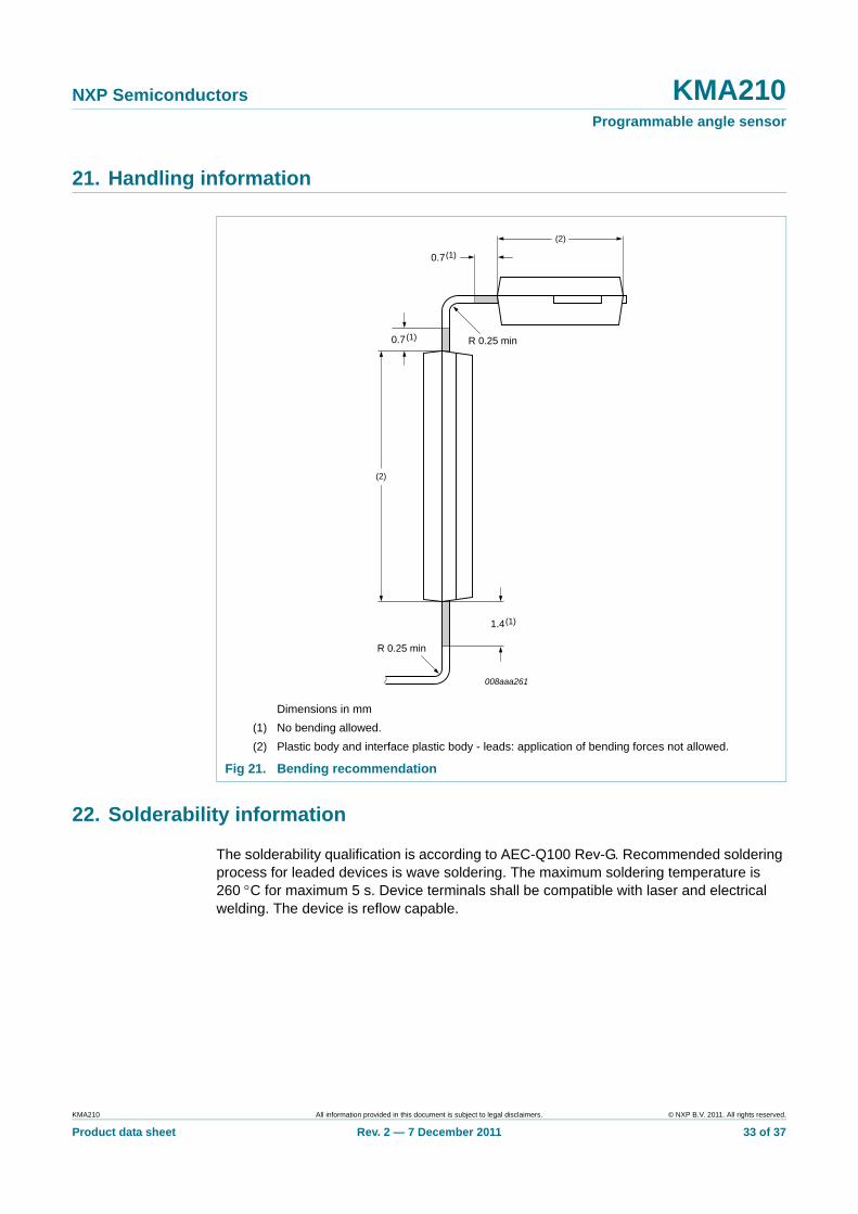
21. Handling information
22. Solderability information
The solderability qualification is according to AEC-Q100 Rev-G. Recommended soldering process for leaded devices is wave soldering. The maximum soldering temperature is 260 C for maximum 5 s. Device terminals shall be compatible with laser and electrical welding. The device is reflow capable.
Dimensions in mm
(1) No bending allowed.
(2) Plastic body and interface plastic body - leads: application of bending forces not allowed.
Fig 21. Bending recommendation
008aaa261
R 0.25 min
R 0.25 min
0.7(1)
1.4(1)
0.7(1)
(2)
(2)
KMA210 All information provided in this document is subject to legal disclaimers. © NXP B.V. 2011. All rights reserved.
Product data sheet Rev. 2 — 7 December 2011 33 of 37
NXP Semiconductors KMA210Programmable angle sensor
23. Revision history
Table 28. Revision history
Document ID Release date Data sheet status Change notice Supersedes
KMA210 v.2 20111207 Product data sheet - KMA210 v.1
Modifications: • Table 6 “Diagnostic behavior”: Power-loss duration changed
• Section 19 “Terminals”: Lead finish information removed
KMA210 v.1 20110630 Product data sheet - -
KMA210 All information provided in this document is subject to legal disclaimers. © NXP B.V. 2011. All rights reserved.
Product data sheet Rev. 2 — 7 December 2011 34 of 37

NXP Semiconductors KMA210Programmable angle sensor
24. Legal information
24.1 Data sheet status
[1] Please consult the most recently issued document before initiating or completing a design.
[2] The term ‘short data sheet’ is explained in section “Definitions”.
[3] The product status of device(s) described in this document may have changed since this document was published and may differ in case of multiple devices. The latest product status information is available on the Internet at URL http://www.nxp.com.
24.2 Definitions
Draft — The document is a draft version only. The content is still under internal review and subject to formal approval, which may result in modifications or additions. NXP Semiconductors does not give any representations or warranties as to the accuracy or completeness of information included herein and shall have no liability for the consequences of use of such information.
Short data sheet — A short data sheet is an extract from a full data sheet with the same product type number(s) and title. A short data sheet is intended for quick reference only and should not be relied upon to contain detailed and full information. For detailed and full information see the relevant full data sheet, which is available on request via the local NXP Semiconductors sales office. In case of any inconsistency or conflict with the short data sheet, the full data sheet shall prevail.
Product specification — The information and data provided in a Product data sheet shall define the specification of the product as agreed between NXP Semiconductors and its customer, unless NXP Semiconductors and customer have explicitly agreed otherwise in writing. In no event however, shall an agreement be valid in which the NXP Semiconductors product is deemed to offer functions and qualities beyond those described in the Product data sheet.
24.3 Disclaimers
Limited warranty and liability — Information in this document is believed to be accurate and reliable. However, NXP Semiconductors does not give any representations or warranties, expressed or implied, as to the accuracy or completeness of such information and shall have no liability for the consequences of use of such information.
In no event shall NXP Semiconductors be liable for any indirect, incidental, punitive, special or consequential damages (including - without limitation - lost profits, lost savings, business interruption, costs related to the removal or replacement of any products or rework charges) whether or not such damages are based on tort (including negligence), warranty, breach of contract or any other legal theory.
Notwithstanding any damages that customer might incur for any reason whatsoever, NXP Semiconductors’ aggregate and cumulative liability towards customer for the products described herein shall be limited in accordance with the Terms and conditions of commercial sale of NXP Semiconductors.
Right to make changes — NXP Semiconductors reserves the right to make changes to information published in this document, including without limitation specifications and product descriptions, at any time and without notice. This document supersedes and replaces all information supplied prior to the publication hereof.
Suitability for use in automotive applications — This NXP Semiconductors product has been qualified for use in automotive applications. Unless otherwise agreed in writing, the product is not designed,
authorized or warranted to be suitable for use in life support, life-critical or safety-critical systems or equipment, nor in applications where failure or malfunction of an NXP Semiconductors product can reasonably be expected to result in personal injury, death or severe property or environmental damage. NXP Semiconductors accepts no liability for inclusion and/or use of NXP Semiconductors products in such equipment or applications and therefore such inclusion and/or use is at the customer's own risk.
Applications — Applications that are described herein for any of these products are for illustrative purposes only. NXP Semiconductors makes no representation or warranty that such applications will be suitable for the specified use without further testing or modification.
Customers are responsible for the design and operation of their applications and products using NXP Semiconductors products, and NXP Semiconductors accepts no liability for any assistance with applications or customer product design. It is customer’s sole responsibility to determine whether the NXP Semiconductors product is suitable and fit for the customer’s applications and products planned, as well as for the planned application and use of customer’s third party customer(s). Customers should provide appropriate design and operating safeguards to minimize the risks associated with their applications and products.
NXP Semiconductors does not accept any liability related to any default, damage, costs or problem which is based on any weakness or default in the customer’s applications or products, or the application or use by customer’s third party customer(s). Customer is responsible for doing all necessary testing for the customer’s applications and products using NXP Semiconductors products in order to avoid a default of the applications and the products or of the application or use by customer’s third party customer(s). NXP does not accept any liability in this respect.
Limiting values — Stress above one or more limiting values (as defined in the Absolute Maximum Ratings System of IEC 60134) will cause permanent damage to the device. Limiting values are stress ratings only and (proper) operation of the device at these or any other conditions above those given in the Recommended operating conditions section (if present) or the Characteristics sections of this document is not warranted. Constant or repeated exposure to limiting values will permanently and irreversibly affect the quality and reliability of the device.
Terms and conditions of commercial sale — NXP Semiconductors products are sold subject to the general terms and conditions of commercial sale, as published at http://www.nxp.com/profile/terms, unless otherwise agreed in a valid written individual agreement. In case an individual agreement is concluded only the terms and conditions of the respective agreement shall apply. NXP Semiconductors hereby expressly objects to applying the customer’s general terms and conditions with regard to the purchase of NXP Semiconductors products by customer.
No offer to sell or license — Nothing in this document may be interpreted or construed as an offer to sell products that is open for acceptance or the grant, conveyance or implication of any license under any copyrights, patents or other industrial or intellectual property rights.
Document status[1][2] Product status[3] Definition
Objective [short] data sheet Development This document contains data from the objective specification for product development.
Preliminary [short] data sheet Qualification This document contains data from the preliminary specification.
Product [short] data sheet Production This document contains the product specification.
KMA210 All information provided in this document is subject to legal disclaimers. © NXP B.V. 2011. All rights reserved.
Product data sheet Rev. 2 — 7 December 2011 35 of 37

NXP Semiconductors KMA210Programmable angle sensor
Export control — This document as well as the item(s) described herein may be subject to export control regulations. Export might require a prior authorization from competent authorities.
24.4 TrademarksNotice: All referenced brands, product names, service names and trademarks are the property of their respective owners.
25. Contact information
For more information, please visit: http://www.nxp.com
For sales office addresses, please send an email to: [email protected]
KMA210 All information provided in this document is subject to legal disclaimers. © NXP B.V. 2011. All rights reserved.
Product data sheet Rev. 2 — 7 December 2011 36 of 37

NXP Semiconductors KMA210Programmable angle sensor
26. Contents
1 Product profile . . . . . . . . . . . . . . . . . . . . . . . . . . 11.1 General description . . . . . . . . . . . . . . . . . . . . . 11.2 Features and benefits . . . . . . . . . . . . . . . . . . . . 1
2 Pinning information. . . . . . . . . . . . . . . . . . . . . . 2
3 Ordering information. . . . . . . . . . . . . . . . . . . . . 2
4 Functional diagram . . . . . . . . . . . . . . . . . . . . . . 3
5 Functional description . . . . . . . . . . . . . . . . . . . 45.1 Angular measurement directions . . . . . . . . . . . 4
6 Analog output. . . . . . . . . . . . . . . . . . . . . . . . . . . 5
7 Diagnostic features . . . . . . . . . . . . . . . . . . . . . . 67.1 CRC and EDC supervision . . . . . . . . . . . . . . . . 67.2 Magnet-loss detection . . . . . . . . . . . . . . . . . . . 67.3 Power-loss detection . . . . . . . . . . . . . . . . . . . . 67.4 Broken bond wire detection . . . . . . . . . . . . . . . 77.5 Low supply voltage detection and overvoltage
protection . . . . . . . . . . . . . . . . . . . . . . . . . . . . . 7
8 Limiting values. . . . . . . . . . . . . . . . . . . . . . . . . . 8
9 Recommended operating conditions. . . . . . . . 9
10 Thermal characteristics . . . . . . . . . . . . . . . . . . 9
11 Characteristics. . . . . . . . . . . . . . . . . . . . . . . . . . 9
12 Definition of errors. . . . . . . . . . . . . . . . . . . . . . 1312.1 General . . . . . . . . . . . . . . . . . . . . . . . . . . . . . . 1312.2 Hysteresis error . . . . . . . . . . . . . . . . . . . . . . . 1312.3 Linearity error . . . . . . . . . . . . . . . . . . . . . . . . . 1412.4 Microlinearity error . . . . . . . . . . . . . . . . . . . . . 1412.5 Temperature drift error . . . . . . . . . . . . . . . . . . 1412.6 Angular error. . . . . . . . . . . . . . . . . . . . . . . . . . 15
13 Programming . . . . . . . . . . . . . . . . . . . . . . . . . . 1613.1 General description . . . . . . . . . . . . . . . . . . . . 1613.2 Timing characteristics . . . . . . . . . . . . . . . . . . . 1713.3 Sending and receiving data . . . . . . . . . . . . . . 1813.3.1 Write access . . . . . . . . . . . . . . . . . . . . . . . . . . 1913.3.2 Read access. . . . . . . . . . . . . . . . . . . . . . . . . . 2013.3.3 Entering the command mode . . . . . . . . . . . . . 2113.4 Cyclic redundancy check . . . . . . . . . . . . . . . . 2113.4.1 Software example in C . . . . . . . . . . . . . . . . . . 2213.5 Registers . . . . . . . . . . . . . . . . . . . . . . . . . . . . 2313.5.1 Command registers . . . . . . . . . . . . . . . . . . . . 2313.5.2 Non-volatile memory registers . . . . . . . . . . . . 24
14 Electromagnetic compatibility . . . . . . . . . . . . 2714.1 Emission (CISPR 25) . . . . . . . . . . . . . . . . . . . 2714.1.1 Conducted radio disturbance . . . . . . . . . . . . . 2714.1.2 Radiated radio disturbance. . . . . . . . . . . . . . . 27
14.2 Radiated disturbances (ISO 11452-1 third edition (2005-02), ISO 11452-2, ISO 11452-4 and ISO 11452-5). . . . . . . . . . . . . . . . . . . . . . 27
14.2.1 Absorber lined shielded enclosure. . . . . . . . . 2714.2.2 Bulk-current injection . . . . . . . . . . . . . . . . . . . 2714.2.3 Strip line . . . . . . . . . . . . . . . . . . . . . . . . . . . . . 2714.2.4 Immunity against mobile phones . . . . . . . . . . 2814.3 Electrical transient transmission by capacitive
coupling [ISO 7637-3, second edition (2007-07)] . . . . . . . . . . . . . . . . . . . . . . . . . . . 28
15 ElectroStatic Discharge (ESD) . . . . . . . . . . . . 2915.1 Human body model (AEC-Q100-002) . . . . . . 2915.2 Human metal model (ANSI/ESD SP5.6-2009) 2915.3 Machine model (AEC-Q100-003). . . . . . . . . . 2915.4 Charged-device model (AEC-Q100-011) . . . . 29
16 Application information . . . . . . . . . . . . . . . . . 30
17 Test information . . . . . . . . . . . . . . . . . . . . . . . 3017.1 Quality information . . . . . . . . . . . . . . . . . . . . . 30
18 Marking . . . . . . . . . . . . . . . . . . . . . . . . . . . . . . 31
19 Terminals . . . . . . . . . . . . . . . . . . . . . . . . . . . . . 31
20 Package outline. . . . . . . . . . . . . . . . . . . . . . . . 32
21 Handling information . . . . . . . . . . . . . . . . . . . 33
22 Solderability information . . . . . . . . . . . . . . . . 33
23 Revision history . . . . . . . . . . . . . . . . . . . . . . . 34
24 Legal information . . . . . . . . . . . . . . . . . . . . . . 3524.1 Data sheet status . . . . . . . . . . . . . . . . . . . . . . 3524.2 Definitions . . . . . . . . . . . . . . . . . . . . . . . . . . . 3524.3 Disclaimers . . . . . . . . . . . . . . . . . . . . . . . . . . 3524.4 Trademarks . . . . . . . . . . . . . . . . . . . . . . . . . . 36
25 Contact information . . . . . . . . . . . . . . . . . . . . 36
26 Contents. . . . . . . . . . . . . . . . . . . . . . . . . . . . . . 37
© NXP B.V. 2011. All rights reserved.
For more information, please visit: http://www.nxp.comFor sales office addresses, please send an email to: [email protected]
Date of release: 7 December 2011
Document identifier: KMA210
Please be aware that important notices concerning this document and the product(s)described herein, have been included in section ‘Legal information’.