Embed Size (px)
Citation preview

KLE.Dr .M.S.SHESHGIRI
COLLEGE OF ENGINEERING & TECHNOLOGY BELAGAVI-08
LIBRARY AND INFORMATION CENTER
QUESTION PAPERS 3rd,4th 5th,6th 7th & gth SEMESTER
ELECTRONICS & COMMUNICATION
JUNE/JULY-2017
KLE Dr. M.S. Sheshgiri College of Engineering & Technology, Library, Belagavi

KLE Dr. M.S. Sheshgiri College of Engineering & Technology, Library, Belagavi

@rn@©~
USN I I I I I I I I I I I 15MAT31
Third Semester B.E. Degree Examination, June/July 2017
Engineering Mathematics - 111
Time: 3 hrs. Max. Marks: 80
1
2
Note: Answer FIVE full questions, choosing onefull question.from each module.
Module-I
a. Obtain the Fourier series expansion of
f(x) = {
rcx O::::; x::::; I
rc(2-x) l::::;x::::;2 (08 Marks)
I l I rc 2
and deduce that ----:, + - 2 + - 2 + · · · · · = - · l" 3 5 8
b. Obtain the constant term and first sine and cosine terms in the Fourier expansion of y from
the following table. (08 Marks)
I~ I ~ I /81 ~41 ~812~ I ~o I OR
a. Expand f(x) = Jxl as a Fourier series in -rc :S x :S rc and deduce that (06 Marks)
l l l re T2+?+sz+ ..... =s·
b. Obtain the half range cosine series for the function f{x) = x sin x in O < x < rc. (05 Marks)
c. The following table gives variations of periodic current over a period T. Show that there is a
direct current part of 0.75 amp in the variable current and obtain the amplitude of first
harmonic. (05 Marks)
t(sec) 0 T T T 2T 5T - - - - -6 3 '" 3 6
A (amp) 1.98 1.3 1.05 1.3 -0.88 -0.25
Module-2
3 a. Find the Fourier Transform of
{
I - x2 Ix I::::; I f(x) =
0 lxl> I
J"' x cos x - sin x xi
Hence evaluate :i cos 72
dx. O x
b. Find the Fourier cosine transform of
{
x for O < x < I
f(x) = 2 -
0
x for I < x < 2
for x > 2
c. Find the inverse Z - transform of
3z2 + 2z
(5z -1)(5z + 2)
I of3
(06 Marks)
(05 Marks)
(05 i\larks)
KLE Dr. M.S. Sheshgiri College of Engineering & Technology, Library, Belagavi

, .. :,,
OR
4 a. Find the Fourier sine transform of e-ax , a> O. x
b. Find the Z - transform of i) cosh ne ii) n2
.
c. Solve the difference equation Yn+2 + 4Yn+1 + 3yn = 3n with Yo= 0, Yi= I.
Module-3
.... 1
15MAT31
(06 Mark1>)
(05 Marks)
(OS Marks)
5 a. Find the coefficient of correlation and two regression lines for the following data: (06 Marks)
x I 2 3 4 5 6 7 8 9 10
y 10 12 16 28 25 36 41 49 40 50
b. Fit a curve of the form y = ae x for the following data : (OS Marks)
I ~ I 1 ~ 3 I s6
s I 21
3 I ~ I ~ I ~0
I c. Use Newton - Raphson method to find a real root of the equation
x sin x + cos x = 0 near x = rr.
OR
(05 Marks)
6 a. In a partially destroyed lab record, only the lines of regression of y on x and x on y are
available as 4x - Sy + 33 = 0 aP.d 20x - 9y = i 07 respectively. Calculate x, y ad
coefficient of correlation between x and y. (06 Marks)
b. Fit a second degree parabola to the following data: (05 Marks)
x 1.0 I .5 2.0 2.5 3.0 3.5 4.0
y 1.1 1.3 1.6 2.0 2.7 3.4 4.1
c. Use the regula - falsi method to obtain a root of the equation 2x - log 10x = 7 which lies
between 3.5 and 4. Carryout 2 iterations. (05 Marks)
]_\,fodule-4
7 a. The population of a town is given by the table (06 Marks)
Year 1951 1961 1971 1981 1991
Population in thou~ands 19.96 39.65 58.81 77.21 94.61
Using Newton's forward and backward interpolation formula, calculate the increase in the
population from the year 1955 to 1985.
b. Use Lagrange's interpolation formula to find y at x = 10, given (05 Marks)
I ~ i 15
2 i 1~1 I 19
41 : ~ I c. Given the values
x 2 4 5 6 8 IO
y 10 96 196 350 868 1746
Construct the interpolating polynomial using Newton's divided difference interpolation
formula. (OS Marks)
OR
8 a. From the fo I lowing table, estimate the number of students who obtained marks bet\veen 40
and 45. (06 Marks)
Marks 30-40 40-50 50-60 60-70 70-80
No. of students 31 42 51 35 31
2 of"3
KLE Dr. M.S. Sheshgiri College of Engineering & Technology, Library, Belagavi

15MAT31
b. Apply Lagrange's formula inversely to obtain the root of the equation flx) = 0, given
f(30) = -30, f(34) = -13, f{38) = 3 . f(42) = 18. (05 Marks) 0.6
c. Use Simpson's ~ rule to find f 3 0
2 e-' dy by taking 7 ordinates. (05 Marks)
Module-5
9 a. Find the work done in moving a particle in the force field F = 3x2
i + (2xz - y)j + z k along
the curve defined by x2
= 4y , 3x3
= 8z from x = 0 to x = 2. (06 Marks)
b. Verify Stoke's theorem for F = (x2 + y2)i - 2xy j around the rectangle x = ± a , y = 0 ,
y = b. (05 Marks)
c. Solve the Euler's equation for the functional r (I+ x2/)y
1dx. (05 Marks)
OR
10 a. Verify Green's theorem for f (xy + y 2)dx + x 2dy, where e is bounded by y = x and y = x2
.
(06 Marks)
b. Evaluate the surface integral f J F. Nds where F = 4xi - 2i.i + z2k and s is the surface
bounding the region x2 + y2 = 4, z = 0 and z = 3. (05 Marks)
c. Show that the shortest distance between any two points in a plane is a straight line. (05 Marks)
* * * * *
3 of3
KLE Dr. M.S. Sheshgiri College of Engineering & Technology, Library, Belagavi

KLE Dr. M.S. Sheshgiri College of Engineering & Technology, Library, Belagavi

@ID@. :.® ~--D D • . o • a i , ·' ~·· ~ , ' • ·, i d • 0 ·~ •4 • •'
USN I I I I I I I I I I I Third Semester B.E. Degree Examination, June/July 2017
Additional Mathematics - I
Time: 3 hrs. Max. Marks: 80
l
2
3
4
5
Note: Answer FIVE full questions, choosing onefull question from each module.
a. Express 3 + 4i in the form x + iy. 3-4i
Module-I
b. Express Jj + i in the polar form and hence find their modulus and amplitudes.
c. Find the sine of the angle between a = 2i- 2j + k and b = i- 2j + 2k.
OR
a. Simplify
(cos30 + i sin 38)4 ( cos40 + i sin 48)5
(cos48 + isin 48) 3 + (cos50 + i sin 58f4
(06 Marks)
(05 Marks)
(05 Marks)
(06 Marks)
b. If a = i + 2j - 3k and b = 3i - j + 2k, then show that ( a + b) and ( a - b) are orthogonal. (05 Marks)
c. Find the value of A, so that the vectors a = 2i - 3j + k, b = i + 2j - 3k and c = j + Ak are
co-planar. (05 Marks)
Module-2 2 ? 2
a. If y = cos (m log x) then prove that x Yn+2 + (2n + 1 )XYn+ 1 + (m- + n ) y 11 = 0.
b. With usual notation prove that
rd8 tan$=-.
dr
(x4+y4J ou ou
c. Ifu = loge , show that x-+ y-= 3. x+y ax oy
OR
a. Find the Pedal equation of r = a[l-cos 0].
b. Expand logc(l+ x) in ascending powers ofx as far as the term containing x4.
c. Find the total derivative of Z = xy2 + x2y, where x = at2 y = 2at.
Module-3
a. Evaluate f sin6
3x dx using Reduction formula. 0
I
b. Evaluate J x 6 "11- x
2 dx - using Reduction formula.
0
1 1-y
c. Evaluate ff xydxdy . I O
OR
I of 2
(06 Marks)
(05 Marks)
(05 Marks)
(06 Marks)
(05 Marks)
(05 Marks)
(06 Marks)
(05 Marks)
(05 Marks)
KLE Dr. M.S. Sheshgiri College of Engineering & Technology, Library, Belagavi

/-'? .)···
15MATDIP31
6 a. Evaluate f sin3 x cos7x dx. (06 Marks)
0
1t
b. Evaluate f x cos6 x dx. (05 Marks)
0
3 2 I
c. Evaluate f f f (x + y + z) dz dx dy. (05 Marks)
0 0 0
Module-4
7 a. A particle moves along the curve r= (l-t3)i + (l+t
2)J + (2t - 5)k. Determine the velocity
and acceleration. (06 Marks)
b. Find the directional derivative of ~ = xy2 + yz3
at the point (2,-1, 1) in the direction of the vector i + 2j + 2k. (05 Marks)
c. Find the constant a, b, c. Such that the vector
F=(x+y+az) i +(x+cy+2z) k +(bx+2y-z)] isirrotational. (05Marks)
OR
8 a. Find the angle between the tangents to the curve r = t2 i + 2t] - t3 k at the points t = ± 1.
b. Find the divergence and curl of the vector - 2 ~ 2 .). ~ , 2 ~
F = (xyz + y z) i + (3x + y z) j + (xz- - y z) k .
c. If F =(ax+ 3y + 4z) i + (x - 2y + 3z)] + (3x + 2y- z) k is solenoidal, find a.
Module-5
9 a. Solve dy y =
x-FY dx
b. Solve dy . - + y cot x = sm x. dx
c. Solve dy x + 2y- l
dx x + 2y + l
OR
10 a. Solve (x2 - y2) dx = 2xy dy.
b. dy 3 6
Sc've ~ dx + y = x y.
c. (1 + xy) ydx + (1 - xy) xdy = 0.
*****
2 of2
(06 Marks)
(05 Marks)
(05 Marks)
(06 Marks)
(05 Marks)
(05 Marks)
(06 Marks)
(05 Marks)
(05 Marks)
KLE Dr. M.S. Sheshgiri College of Engineering & Technology, Library, Belagavi

@.[3@&1~@
USN I I I I I I : I I I I Third Semester B.E. Degree Examination, June/July 2017
Analog Electronics
15EC32
Time: 3 hrs. Max. Marks: 80
Note: Answer any FIVE full questions, choosing ONE full question from each module.
Module-I
1 a. Draw re and h-parameter models of a transistor in common - emitter configuration. Also
give relation between re and h-parameter (05 Marks)
b. Draw the emitter follower circuit. Derive expressions for i) Zi ii) Zo iii) Av using re model. (O~ Marks)
c. Draw and explain the hybrid-1t model of transistor in CE configuration mentioning
significance of each component in model. (05 Marks)
OR
2 a. Derive expressions for Zi, Zo, Av and A1 for common-emitter fixed bias configuration using
hybrid equivalent model. (08 Marks)
b. For the circuit shown below, taking r0 = ooQ calculate i) re ii) Zi iii) Zo iv) Av. (08 Marks)
G·~/)...- l O)".F- ·
ID.J.lf H ox w---1 r~3n
~ l·S-KJL, I I -:::
7 Zo,
Fig.Q2(b)
Module-2
3 a. With circuit diagram of JFET small signal model, determine gm and rd. (08 Marks)
b. For the JFET common-source amplifier using fixed-bias configuration. Derive expressions
for Zi , Zo and Av using AC equivalent circuit. (08 Marks)
1 of3
KLE Dr. M.S. Sheshgiri College of Engineering & Technology, Library, Belagavi

;:~··\ .N :·r·.~-~!--~ , 15EC32 . > 1: .) f3.j~: .'· '
'
OR
4 a. For'°the JFET common-gate configuration shown below, calculate Zi, Zo and Av. (08 l\Iarks)
tls-v
Rp== 3.3)::JL
roJ>.F-.-------1 \-,· o V-o
Fig.Q4(a) b. With neat diagram, explain construction of n-channel JFET, and also draw its
characteristics. (08 Marks)
Module-3
5 a. Describe Miller-effect and derive an equation for miller input and output capacitance. (08 Marks)
b. Discuss low frequency response of BJT amplifier and give expressions for low frequency due to input coupling capacitor Cs and output coupling capacitor Cc. (08 Marks)
OR
6 a. Explain high-frequency response of FET amplifier, and derive expression for cutoff frequencies defined by input and output circuits(fHi and fHo). (08 Marks)
b. For the circuit shown.
Vee= 20V
- 2Jd2- I 2,N
Fig.Q6(b)
ro = oofl, Cn(cbe) = 36pF, Cu (cbc) = 4pF, Cce = 1 pF, Cwi = 6 pF, Cwo = 8pF
i) determine fHiand fi-ro ii) find f13 and fT.
2 of3
(08 Marks)
KLE Dr. M.S. Sheshgiri College of Engineering & Technology, Library, Belagavi

15EC32
Module-4
7 a. What is Barkhauscn criterion? Explain how oscillations start in an oscillator. (04 Marks)
b. With the help of a neat circuit diagram, explain transistor colpitts oscillator. Write the
expression for frequency of oscillations. (08 Marks)
c. A quartz crystal has L = 0.12H, C = 0.04 pf CM= lpF and R = 9.2 kQ, Find:
i) series resonant frequency ii) Parallel resonant frequency. (04 Marks)
OR
8 a. Explain characteristics of a quartz crystal. With a neat diagram explain the crystal oscillator in parallel resonant mode. (08 Marks)
b. The following component values are given for the Wein-bridge oscillator of the circuit of
R, = R2 = 33:kQ C, = C2 = O.OOlµF R3 = 47 kQ, Ri = 15kQ.
i) Will this circuit oscillate? ii) Calculate the resonant frequency. (08 Marks)
Module-5
9 a. Explain series - fed class - A power amplifier. Show that its maximum conversion efficiency is 25%. (08 Marks)
b. Explain with circuit diagram the operation of Class-B push-Pull amplifier using complementary-symmetry transistor pair. Also mention advantages and disadvantages of the circuit. (08 Marks)
OR
10 a. An ideal class -B push-pull power amplifier with input and output transformers has
Yee = 20V, N2 = 2N1 and RL = 200. The transistors has hre = 20. Let the input be
sinusoidal. For the maximum output signal at V CE<P) = V cc, determine : i) The output signal power
ii) The collector dissipation in each transistor iii) Conversion efficiency.
b. The following distortion readings are available for a power amplifier,
D2 = 0.2, D3= 0.02, D4 = 0.06, with I1 = 3.3A and Re= 4Q. i) Calculate the total harmonic distortion
ii) Determine the fundamental power component iii) Calculate the total power.
* * * * *
3 of3
(08 Marks)
(08 Marks)
KLE Dr. M.S. Sheshgiri College of Engineering & Technology, Library, Belagavi

KLE Dr. M.S. Sheshgiri College of Engineering & Technology, Library, Belagavi

C)
0 ;z c 5 .... 0 c..
..§
@ill@®~~
USN I I I I I I I I I I I Third Semester B.E. Degree Examination, June/July 2017
Digital Electronics
Time: 3 hrs. Max. Marks: 80
1
2
3
4
5
6
7
Note: Answer any FIVE full questions, choosing one full.question from each module.
Module-1
a. Convert the given Boolean function into
i) Y = f (a. b, c) =(a+ b) (a+ c) minterm canonical form (04 Marks)
ii) P = f (a, b, c) =(a+ b) (b + c) (c + a) maxterm canonical form. (04 Marks)
b. Using K-map determine the minimal sum of product expression and realize the simplified
expression using only NANO gates.
M = f(W, X, Y, Z) = I (I, 4, 5, 6, 11, 12, 13, 14, 15). (08 Marks)
OR a. Simplify the given Bo6lean function using Quine - McCluskey method:
Y = f(a, b, c, d) = I (0, 2, 3, 5, 8, 10, 11). Verify the result using k-map.
b. Distinguish between prime implicant and Essential prime implicant.
Module-2
(12 Marks)
(04 Marks)
a. Define Decoder. Implement the following multiple output function using IC 74138 and
external gates. Also write the truth table.
P = f1 (X, Y, Z) = L (1, 2, 5, 6) Q = f2 (X, Y, Z) = n (3, 5, 6, 7). (06 :\'forks)
b. Implement the following Boolean function using 8: 1 multiplexer:
Y = f(A, B, C, D) = ABO+ ACD+ BCD+ ACD (10 Marks)
OR a. Design and implement 4-bit look ahead carry adder.
b. Design and implement BCD to Excess-3 code converter.
Module-3
(08 Marks)
(08 Marks)
a. Explain the working principle of gated SR latch. (06 Marks)
b. Explain the working of master slave JK flip-flop with the help of a logic diagram, function
table, logic symbol and timing diagram. (10 Marks)
OR a. With a neat logic diagram, explain the working of positive edge triggered D flip-flop. Also
draw the timing diagram. (08 Marks)
b. Derive the characteristic equation for JK and T flip-flop. (08 Marks)
Module-4 a. Describe the working principle of universal shift register with the help of logic diagram and
mode control table. (08 Marks)
b. Illustrate the operation of 4-bit binary ripple counter using logic diagram and timing
diagram. (08 Marks)
1 of2
KLE Dr. M.S. Sheshgiri College of Engineering & Technology, Library, Belagavi

OR
8 a. Design a synchronous Mod-6 counter using clocked T flip-flop.
b. Explain Mod-4 ring counter using D flip-flop.
Module-5 9 a. Explain Mealy and Moore sequential circuit models.,
b. For the logic diagram shown in I:jg Q 9(b).
i) Write input and output equations
ii) Construct transition table
iii) Draw state diagram.
c.
p
l=1 c.
Clod:-
tJ_
&
Fig Q9(b)
OR
10 a. Define the terms as applied to sequential circuit :
F.2-
!=' I ;i.
Input variable, output variable, Excitation variable and state variable.
b. Design a sequential circuit for a state diagram shown in Fig Q l O(b).
o\O
1\0
,,,
Fig QI O(b)
* * * * * 2 of 2.
15EC33
(IO Marks)
(06 Marks)
(04 Marks)
(12 Marks)
(04 Marks)
(12 Marks)
KLE Dr. M.S. Sheshgiri College of Engineering & Technology, Library, Belagavi

<I)
0 :z
USN
@~@~@llim@
I I I I I I I I I I l Third Semester B.E. Degree Examination, June/July 2017
Network Analysis
15EC34
Time: 3 hrs. Max. Marks: 80
1
2
3
4
Note: Answer any FIVE full questions, choosing ONE full question from each module.
Module-1
a. Calculate the current through 20. resistor for the circuit shown in Fig.Q l(a) using source transformation. (08 Marks)
b. Use mesh analysis to determine the three mesh currents 11, h and h in the circuit shown in Fig.Ql(b). (08 Marks)
1-S Pi
Fig. Q 1 ( a) ,______..__~----l.--! Fig.Ql(b)
OR
a. Find the equivalent resistance RAB using star and delta transformation for network shown in Fig.Q2(a). (08 Marks)
5.11...
f\~\&J\.
l!,.~lilJL
Fig.Q2(a) 6.JL Fig.Q2(b) b. For the circuit shown in Fig.Q2(b), determine all node voltages. (08 Marks)
Module-2 a. Using Millman's theorem, find the current through load resistance RL for the circuit shown
in Fig.Q3(a). (08 Marks)
-J\0 A.
ts~·,; 2. Q .Jl_
Fig.Q3(a)
b. State the maximum power transfer theorem and also prove that 2
P = Vth where max 4RL'
Vth = thevenins voltage.
OR
a. Obtain the Thevenin's equivalent of the circuit shown in Fig.Q4(a).
b. Using superposition theorem, find the current in 6Q. resistor in the Fig.Q4(b).
Fig.Q4(a)
lOOV
.2.o J')... v,
L-----.L.-----0 !:, Fig.Q4(b) 1 of 2
(08 Marks)
(08 Marks)
network shown in (08 Marks)
KLE Dr. M.S. Sheshgiri College of Engineering & Technology, Library, Belagavi

15EC34 i ,_' ,- r! ~¥,. 'iv· Module-3
., . ·'"1,1 ,:<:1 ',(·,~ 5 ·p,< )n the ngt\,:drk shown in Fig.Q5(a), the switch is closed at t = 0, determine
. ·.·. ..,. -,. .
. di d 2i 1-and-at 'dt dt2 ~ ' .-,,.. : ,-:· .
r = ·o,. (08 Marks)
b. For the nct\\'ork shO\rn in Fig.Q5(b), the switch 's' is opened at t = 0 solve for V, DV and D
2V at t = o·. (08 Marks)
\. 0 \I Fig.Q5(a)
,; OR
Fig.Q5(b)
t=-0 IA
6 a. Find the Laplace transform of the periodic signal x(t) shown in Fig.Q6(a). (08 Marks)
{
3, t < 0
b. Given the signal x(t) = -2 0 < t < I
2t-4 t>l
Express x(t) interms of singularity functions. Also find the Laplace transform ofx(t).
x (t) ~- - - - - -
-
1
"""""1'----l-~t\___,_f--_\\___,~· ·_· ·_· _::, r(s et)
Fig.Q6(a) 0 i 1 ~ ~
Module-4
(08 Marks)
7 a. Derive the expressions of half power frequencies W 1 and W2 and also bandwidth of a series
resonance circuit. (09 Marks)
b. Find the values of 1 at which the circuit shown in Fig.Q7(b) resonates at a frequency of
500 r/s. (07 Marks)
Fig.Q7(b)
OR
.2.JL L
8 a. Derive the expressions of a resonance frequency and dynamic impedance of a parallel
9
resonance circuit. (09 Marks)
b. A coil has a R = 20Q, 1 = 80mH and C = I OOpF are connected in series. Determine :
i) impedance at resonance ii) resonance frequency iii) quality factor iv) circuit current if supply voltage is 50V. (07 Marks)
Module-5 a. Derive the expression of Z-parameters in term ofh-parameter. (07 Marks)
b. Find the ABCD - parameters for the network shown in Fig.Q9(b). (09 Marks)
4 t' I Jl._ '4f- i..:2 ._-:;' 2 .11.. ~ "C.. 1
I~ I~ --.--:k~ l I Fig.Q9(b) v, J IF IF J '- Fig.QIO(a) v, }'"" J>n. Y''' ~
1
OR
10 a. Find the Y-parameter for the two port network shown in Fig.QIO(a).
b. Obtain the expression of h-parameters in terms of Y-parameters.
(08 Marks)
(08 Marks)
* * * 2 of 2* * *
KLE Dr. M.S. Sheshgiri College of Engineering & Technology, Library, Belagavi

8 0
z
~IB©©~~: USN I I I I I I l I I I
15EC35
Third Semester B. E Degree Examination, June/July 2017
Electronic Instrumentation
Time: 3 hrs. Max. Marks: 80
1
2
3
4
5
Note: Answer any FIVE full questions, choosing one full question from each module.
Module-I
a. Define types of static errors. How do you avoid them? (06 Marks)
b. Design a multi-range ammeter with range of O - lA, SA and lOA employing individual shunt in each AD' Arsonval movement with an internal resistance of SOOQ arid a 1ull scale
deflection of 1 OmA is available. (05 Marks)
c. Define principle operation of thermocouple, and also explain types of thermocouple. (05 Marks)
OR a. What is loading effect? (02 Marks)
b. Calculate series connected multiplier resistances with a D' Arsonval movement with an
internal resistance of lOOQ and a full scale deflection of lOmA into a multirange de voltmeter with ranges from 0-SV, 0-SOV and 0-lOOV. (04 Marks)
c. Explain Differential voltmeter with circuit. (05 Marks)
d. Explain the working of a true RMS voltmeter with the help of a suitable block diagram. (05 Marks)
Module-2 a. With neat block diagram explain Dual slope integrating meter, and also derive the unknown
voltage equation. (08 Marks)
b. An integrator contains a lOOKQ and lµF capacitor, if the voltage applied to the integrator input is lV, what voltage will be present at the output of the integrator after lsec? (02 Marks)
c. With block diagram, explain principle operation of staircase ramp (06 Marks)
OR a. With neat circuit diagram, explain basic frequency measurement operation. b. Explain with block diagram Digital phase meter operation. c. Define Tachometer and pH meter.
Module-3 a. With neat circuit diagram explain time base generator with waveform.
b. Explain in detail the working of digital storage oscilloscope and list advantages.
OR
(06 Marks)
(06 Marks)
(04 Marks)
(06 Marks)
(10 Marks)
6 a. Explain with diagram conventional standard signal generator.
b. Explain in detail the working of a function generator.
(OS Marks)
(08 Marks)
l of2
KLE Dr. M.S. Sheshgiri College of Engineering & Technology, Library, Belagavi

' _;, ·;_'. ·· ... ·:,: t// 15EC35
Module-4
7 a. With circuit diagram explain Q - meter and its purpose. (05 i\Jarks)
b. Self capacitance of a coil is measured, if the first measurement is at f, = lMHz and
C 1 = 500pf. The second measurement is at fi = 2MHz and C2 = l lOpf. Find the distributed
capacitance also calculate the value of L. (04 Marks)
c. Define Megger instrument. With circuit diagram explain megger. (07 Marks)
OR
8 a. Define use of Maxwell's bridge. With circuit diagram derive and explain Maxwell's bridge
equation. 0
(08 Marks)
b. A wein bridge circuit consists of the following components R 1 = 4.7 Kn, C1 = 5nf,
R2 = 20KQ, C3 = lOnf, R3 = lOKn, Ri = _100KQ. Determine the frequency of the circuit. (02 Marks)
c. Explain in detail with circuit Wagner's earth connection. (06 Marks)
Module-5
9 a. What are the factors to be considered for the select•ion of transducer?
b. Explain principle operation of resistive position transducer.
c. Explain resistive thermometer, list the advantages.
OR
10 Briefly write a note on :
a. Strain gauges
b. Differential output transducer
c. Piezoelectrical transducer
d. Semiconductor photo diode.
* * * * *
2 of2
(06 Marks)
(04 Marks)
(06 Marks)
(04 Marks)
(04 Marks)
(04 Marks)
(04 !\larks)
KLE Dr. M.S. Sheshgiri College of Engineering & Technology, Library, Belagavi

E 0
;z: E cQ
t:: 0 0.
.§
~~~·~~~0 ~~~~
USN I I I I I I I I I I I 15EC36
Third Semester B.E. Degree Examination, June/July 2017
Engineering Electromagnetics
Time: 3 hrs. Max. Marks: 80
1
2
3
4
5
6
Note: Answer any FIVE full questions, choosing one full question from each module.
Module-1
a. State vector form of Coloumb's law of force between two point charges and indicate the
units of the quantities in the equation. (04 Marks)
b. Let a point charge Q 1 = 25nC be located at A(4, -2, 7) and charge 02 = 60nC be at ----> ---->
B( -3, 4, -2). Find Eat C(l, 2, 3) and find the direction of E.
c. Define electric field intensity due to number of point charge in a vector form.
OR a. Derive an expression for the electric field intensity due infinite line charge.
---->
(10 Marks)
(02 Marks)
(06 Marks)
b. Define electric flux density. Find Din Cartesian co-ordinate system at a point p(6, 8, - 10)
due to a point charge of 40mC at the origin and a uniform line charge of PL= 40µC/m on the
z-axis. (10 Marks)
Module-2 a. State and prove Gauss law as applied to an electric field. (06 Marks)
b. Given that .~ = 30e-r a, - 2za, in the cylindrical co-ordinates. Evaluate both sides of the
divergence theorem for the volume enclosed by r = 2, z = 0 and z = 5. (10 Marks)
OR a. Define the electric scalar potential. Derive an expression for potential due to point charge.
(06 Marks)
b. A point charge of 6nC is located at the origin in free space find potential of point P if P is
located at (0.2, -0.4, 0.4) and i) V =Oat infinity ii) V = 0 at (I, 0, 0) iii) V = 20V at
( -0.5, I, -1 ). (10 Marks)
Module-3 a. Starting with point form of Gauss law deduce Poisson's and Laplace's equation. (03 Marks)
b. State and Prove uniqueness theorem (05 Marks)
c. Find V at (2, 1, 3) for the field of
i) 2 co-axial conducting cylinders V = 20V at p = 3m
ii) 2 concentric conducting spheres V = 50V at r = 3m and V = 20V at r = 5m. (08 Marks)
OR a. State and explain Biot - Savart's law. (04 Marks)
---->
b. Evaluate both sides of the Stoke's theorem for the field H = 6xyax -3/a) Alm and the
rectangular path around the region, 2 ~ x:::; 5,-1:::; y:::; l,z = 0. Let the positive direction of
-;
ds be a . 7.
(08 Marks)
I of2
KLE Dr. M.S. Sheshgiri College of Engineering & Technology, Library, Belagavi
J .. ~· ,;: '_f {1 k:.~?~f~~t, •: c,\" "t ··.·, ?f~.i,.f:,_:\f(il::- Ji'.' __ .,··~-
L ',~:J ,I
15EC36
--->
c. At a point p(x, y, z) the components of \ ector magnetic potential A are given as
--->
A~ ==4x+3y+2z, AY =5x+6y+3z and A, =2x+3y+5z. Determine Bat point P.
(04 Marks)
Module-4 7 a. A point charge of Q = -1.2C has velocity
8
V = (sa, + 2ay -3a,} m Is. Find the magnitude of the force exerted on the charge -if
---> i) E =-18a, + 5ay -!Oa
2 V /m
ii) B=-4a,+4ay+3a, T
iii) Both aie present simultaneously. (08 Marks)
b. Derive an expression for the force on a differential current element placed in a magnetic
field. (04 Marks)
c. A conductor 4m long Ii.es along the y-axis with a current of I O.OA in the a Y direction. Find
---> the force on the conductor if the field in the region is B = 0.005 a, T .
OR
---> a. If B = 0.05xayTin a material for which x
111 == 2.5. Find
-> -> _, ii)µ iii) H iv) M v) J
b. Write a en magnetic circuits
c. Write a note on forces on magnetic materials.
Module-5
(04 Marks)
(08 Marks)
(04 :V1:irks)
(04 Marks)
9 a. Explain Displacement current density and conduction current density. (04 Marks)
b. List Maxwell's equations for steady and time varying fields in
i) Point form ii) Integral from. (06 Marks)
c. Do the fields E ==Em sin x sin tay and H = Em cos x cos taz satisfy Maxwell's equations? ~Lo
OR
10 a. What is Forward travelling wave and Backward travelling wave in free space?
b. A uniform plane wave in free space is given by Es= 200 /30' -e-j2502 a, V/m.
---> Find p, w. f, A, YJ, I H I
c. State and prove Poynting theorem
* * * * *
2 of2
(06 Marks)
(02 Marks)
(06 Marks)
(08 Marks)
KLE Dr. M.S. Sheshgiri College of Engineering & Technology, Library, Belagavi

~~h~,~~ ~~~~uui~
USN I I I I I I I I I I I 15MAT41
Fourth Semester B.E. Degree Examination, June/July 2017
Engineering Mathematics-IV
Time: 3 hrs. Max. Marks: 80
1
2
3
Note: 1. Answer FIVE full questions, choosing one full question from each module.
2. Use of statistical tables are permitted.
Module-1
a. Find by Taylor's series method the value ofy at x = 0.1 from:: =x2y-l, y(O)=l (upto
4th degree term). (05 Marks)
b. The following table gives the solution of 5xy' + y2 -2 = 0. Find the value of y at x = 4.5
using Milne's predictor and corrector formulae. (05 Marks)
I ~ I ~ I 1.~0
1
49 I 1.~g97 ! 1.~-1
3
4311.~·1:71
c. Using Euler's modified method. Obtain a solution of the equation :: = x +!FYI, with initial
conditions y = 1 at x = 0, for the range O::::: x::::; 0.4 in steps of 0.2. (06 Marks)
OR
a. Using modified Euler's method find y(20.2) and y(20.4) given that dy = log10(~) with
dx y
y(20) = 5 taking h = 0.2. (05 Marks)
b. Given dy =x 2 (1+y) and y(l) = l, y(l.l) = 1.233, y(l.2) =1.548, y(J.3) = l.979. Evaluate dx
y(l.4) by Adams-Bashforth method. (05 Marks)
d 2 2
c. Using Runge-Kutta method of fourth order, solve _)'_ = y - x with y(O) = 1 at x = 0.2 by dx y2 +x 2
taking h = 0.2 (06 !\'larks)
Module-2
d2
d a. Obtain the solution of the equation 2--1:. = ux + _)'_ by computing the value of the
dx2
dx
dependent variable corresponding to the value 1.4 of the independent variable by applying
Milne's method using the following data: (05 Marks)
x 1 1.1 1.2 1.3
y 2 2.2156 2.4649 2.7514 I
2 2.3178 2.6725 3.0657 y
b. Express f(x) = 3x3 - x 2 + 5x - 2 in tenns of Legendre polynomials. (05 Marks)
c. Obtain the series solution of Bessel's differential equation x 2y" + xy' + (x 2 + n 2 )y = O
(06 Marks)
l of 3
KLE Dr. M.S. Sheshgiri College of Engineering & Technology, Library, Belagavi

4
.-,
15MA' Al
OR
d2
y (dy)2
2 a. By Runge-Kutta method solve -? = x - -y for x = 0.2. Correct to four decimal dx- dx
places using the initial conditions y = 1 and y' = 0 at x = 0, h = 0.2.
b. Prove that J 1 (x) = /2 sin x
+2 f~ c. Prove the Rodrigues formula,
1 d0
(x2 -1) 0
Pn(x)=-2" ' d" 11. X
Module-3
(05 Marks)
(05 Marks)
(06 Marks)
5 a. State and prove Cauchy's-Riemann equation in polar form. (05 Marks)
(05 Marks)
6
b. Discuss the transformation W = e2 •
E 1 f {sin (rcz
2 )+_ cos(rcz
2 )r c. va uate , z c (z-1)-(z-2)
using Cauchy's residue theorem where 'C' is the circle lzl = 3
OR sin2x
a. Find the analytic function whose real part is, -----cosh2y - cos 2x
(06 Marks)
(05 Marks)
b. State and prove Cauchy's integral formula. (05 Marks)
c. Find the bilinear transformation which maps z = co, i, 0 into ro = -1, -i, 1. Also find the fixed
points of the transformation. (06 Marks)
Module-4
7 a. Find the mean and standard deviation of Poisson distribution. (05 Marks)
b. In a test on 2000 electric bulbs, it was found that the life of a particular make was normally
distributed with an average life of 2040 hours and S.D of 60 hours. Estimate the number of
bulbs likely to burn for, (i) more than 2150 hours. (ii) less than 1950 hours (iii) more than 1920 hours and less than 2160 hours. [A( 1.833) = 0.4664, A( 1.5) = 0.4332, A(2) = 0.4772] (05 Marks)
c. The joint probability distribution of two random variables x and y is as follows:
x/y -4 2 7
1 1/8 1/4 1/8
5 1/4 1/8 1/8
Determine:
( i) Marginal distribution of x and y. (ii) Covariance of x and y
(iii) Correlaiton of x and y.
2 of3
(06 Marks)
KLE Dr. M.S. Sheshgiri College of Engineering & Technology, Library, Belagavi

8
15MAT41
OR
a.
manufactured what is the probability that, (i) Exactly 2 are defective ( ii) at least 2 are
defective (iii) none of them are defective. (OS Marks)
b. Derive the expressions for mean and variance of binomial distribution. (05 Marks)
c. A random variable X take the values -3, -2, -1, 0, 1, 2, 3 such that P(x = 0) = P(x < 0) and
P(x = -3) = P (x = -2) = P(x = -1) = P(x = 1) = P(x = 2) = P(x = 3). Find the probability
distribution. (06 Marks)
Module-5
9 a. In 324 throws of a six faced 'die' an odd number turned up 181 times. Is it reasonable to
think that the 'die' is an unbiased one? (OS Marks)
b. Two horses A and B were tested according to the time (in seconds) to run a particular race
with the following results:
Horse A: 28 30 32 33 33 29 34
Horse B: 29 30 30 24 27 29
Test whether you can discriminate between the two horses.(t0_05=2.2 and t0.o2=2.72 for 11 d. t) (OS Marks)
c. Find the unique fixed probability vector for the regular stochastic matrix, A= j: ~- :1 l O }< Yi
10 a. Define the terms: (i) Null hypothesis
limits.
OR
(ii) Type-I and Type-II error
(06 Marks)
( iii) Confidence
b. Prove that the Markov chain whose
(OS Marks)
t.p.m P = j: ~ ~1 is irreducible. Find the
ly; y; o corresponding stationary probability vector. (05 Marks)
c. Three boys A, B, C are throwing ball to each other. A always throws the ball to B and B
always throws the ball to C. C is just as likely to throw the ball to B as to A. If C was the
first person to throw the ball find the probabilities that after three throws (i) A has the ball.
(ii) B has the ball. (iii) C has the ball. (06 Marks)
* * * * *
3 of3
KLE Dr. M.S. Sheshgiri College of Engineering & Technology, Library, Belagavi

I .
KLE Dr. M.S. Sheshgiri College of Engineering & Technology, Library, Belagavi

OJ
.g u
"' .... 0. :;; E
"' "' -0
B
"' OJ b
ui C)
~..o "" :::: O.·-
..><! ?,: :::: 0 "" :!3
V)
l;(J II oc
:::: + N -~ "1"
:::: e.ii u u .... ;:! t:::
-;:::; e 3
·;::: ?,:
v,
"' u ;.§
:::: .s
c/; ~ v, ::: 2 0-u 0 ... "' -2 § -0 OD t:::
"' "' :s .... 0
?,: ~ "' ~ ... -;:; -0
2' ;:,-0
0 g er. -;:;
~ !l.)
0. 0.
0 "' u d' i .s dJ <j ?,: (.)
v: s § i:: ... <!)
:::: -0 0 ·-;:,-.. ....... OJl O :::: co -~ ;§ 0. "' 0)
E ;:,-
0 0
u ... >-. c I'.::
0 < - N
d)
0 z c "' t:: 0 0.
!::
11
USN
Fourth Semester B.E. Degree Examination, June/July 2017
Additional Mathematics - II
Time: 3 hrs. Max. Marks: 80
1
Note: Answer any FIVE full questions, choosing
ONE full question from each module.
Module-I
a. Find the rank of the matrix :
2 3 21 3 5 l by elementary row transformations.
3 4 5
b. Solve the following system of equations by Gauss elimination method:
2x + y + 4z = 12
4x + 11 y - z = 33
(06 Marks)
8x - 3y + 2z = 20. (OS Marks)
c. Find all the eigenvalues and eigenvector corresponding to largest eigcn value of the matrix :
li : :l (OS Macks)
OR
2 a. Solve the following system of equations by Gauss elimination method:
x+y+z=9
3
4
2x + y-z = 0
2x + Sy+ 7z = 52.
b. Reduce the matrix I~ ;v ; 1 into its echelon form and hence find its rank.
L ~ ..I J
c. Find the inverse of the matrix A = [ ~ ; J using Cayley -- Hami !ton theorem.
a.
b.
c.
a.
b.
Module-2 Solve (0 2
- 40 + 13)y = cos 2x by the method of undetermined coefficients.
Solve (02 + 20 + 1 )y = x2
+ 2x.
Solve (02 - 60 + 25)y = sin x.
OR
Solve (02 + 1 )y = tan x by the method of variation of parameters. ' -1 Solve (0 + 8)y = x + 2x + I.
c. Sol\'c (02 ~ 20 ..... 5)y = c 'cos 2x.
I of 3
(06 Marks)
(05 Marks)
(OS Marks)
(06 Marks)
(OS Marks)
(05 Marks)
(06 Marks)
(OS Marks)
(05 Marks)
-~,.
KLE Dr. M.S. Sheshgiri College of Engineering & Technology, Library, Belagavi

5
•. ; .• 1 ~ •
. -~. , .. ·
Module-3 a. Find the Laplace transforms of:
b. Find:
i) L[ t -Yz + tli J
cos 2t - cos3t ii)-----
t
ii) L[sin St· cos 2t].
c. Find the Laplace transform of the function
t{t+ co)= f(t).
OR
151VIATDIP41
(06 Marks)
(05 Marks)
f(t) = Esin(~t} 0 < t <co, given that
(05 Marks)
6 a. Find:
7
i) Llt2
sin t J (06 Marks)
00
cos6t - cos4t . b. Evaluate : J t dt usmg Laplace transform. (05 Marks)
0
f sin 2t, c. Express f (t) = 1
L 0,
O<t<TC , in tei-.1iS ofunic step function and hence find L[f(t)].
t > TC
Module-4 2
a. Solve the initial value problem d Y 5dy 'X -+-+ 6y = se- , y(O) = 2, y'(O) = I dx2 dx
transforms.
b. Find the inverse Laplace transforms :
? ')
i) 3(s- - J)-
2s2
i s2 + 4 ] c. Find the inverse Laplace transform: logl .
s(s+4)(s-4)
OR
s+l ii)----
s2 +6s +9.
(05 Marks)
using Laplace
(06 Marks)
(05 Marks)
(05 Marks)
8 a. Solve the initial value problem :
2
d ; + 4
dy + 3y = e-t with y(O) = I = y' (0) using Laplace transforms. dt dt
(06 Marks)
b. Find the inverse Laplace transform : . 1 3 8 1)--+----
sJs s2 Js Js .. ) 3s + l 11 2 .
(s-l)(s +I) (05 Marks)
2s-l Find the inverse Laplace transform: -.,----.
s- +4s+29 c. (05 Marks)
2 of 3
KLE Dr. M.S. Sheshgiri College of Engineering & Technology, Library, Belagavi

Module-5
9 a. State and prove Baye's theorem. (06 Marks)
b. A can hit a target 3 times in 5 shots, B 2 times in 5 shots and C 3 times in 4 shots. They fire
a volley. What is the probability that i) two shots hit ii) at least two shots hit? (05 Marks)
7 c. Find P(A), P(B) and P(A n B), if A and B are events with P(A u B) = - ,
8 1 - 5
P(A n B) =-and P(A) =-. 4 8
(05 Marks)
OR
10 a. Prove that P(AUB) = P(A) + (B) - P(MB), for any two events A and B. (06 Marks)
b. Show that the events A and B are independent, if A and B are independent events. (05 Marks)
c. Three machines A, B and C produce respectively 60%, 30%, 10% of the total number of
items of a factory. The percentage of defective output of these machines arc respectively
2%, 3% and 4%. An item is selected at random and is found defective. Find the probability
that the item was produced by machine C. (05 !\larks)
* * * * *
3 of 3
KLE Dr. M.S. Sheshgiri College of Engineering & Technology, Library, Belagavi

KLE Dr. M.S. Sheshgiri College of Engineering & Technology, Library, Belagavi

2 0
z c e 0 a. .§
(i)~~~ ~t~1'~~ ~U~'
' \ \
USN I I I I I I I I I I I 15EC42
Fourth Semester B.E. Degree Examination, June/July 2017
Microprocessor
Time: 3 hrs. Max. Marks: 80
1
2
3
4
Note: Answer FIVE full questions, choosing one full question from each module.
Module-1
a. Explain the internal architecture of 8086 with its neat block diagram. (08 Marks)
b. Explain briefly any 4 addressing modes of data of 8086 with an example for each. (06 Marks)
c. If CS= 1000 H, DS = 25AOH, SS= 3210H, ES= 5890H, BX= 43A9H, BP= 3400H, find the physical address of the source data for the following instrnctions:
(i) MOV AL, [BX+1200H] (ii) ADD BL, [BP+05] (02 Marks)
OR
a. Write down the instruction formats for the following two types of cases of 8086 and form the opcode for the indicated instruction:
(i) Register to Register; ADD AX, BX (ii) !mmec!.iate to Register; ADD CX, 1200 H. (06 Marks)
b. Write 8086 program to find the smallest number out of N 16 bit unsigned numbers stored in a memory block starting with the address 2000 H. Store the result at word location 3000 H.
(08 Marks)
c. Briefly explain the following 8086 instructions:
a.
(i) XLAT (ii) NEG (02 Marks)
Module-2
Write a complete assembly language program in 8086 which replaces all the occurances of character'-' in a given"string by'*'. (08 Marks)
b. Verify whether any of the following instructions are wrong and correct them with reasons.
Assuming following is a program, what is the value of register BX and flags CY, Z, P, S at
the end. (i)
(ii) ( iii) (iv)
(v)
MOY BX, 0804H
INC [BX+02] ADD 06H, AL
SHRDX, 02 XOR BL, BL (08 Marks)
OR
a. Briefly explain the operations of the string instructions of 8086, indicating the initializations required to use them. (06 Marks)
b. Write a complete assembly language program for block move of a source data (10 bytes)
present in a memory block sta11ing with address SOURCE to a destination block sta11ing
from address DSTN, using MOVS instruction. Consider overlapping ofblocks also.
c. Explain briefly any -1- :1ssembler directives.
l of 2
(08 Marks)
(02 Marks)
KLE Dr. M.S. Sheshgiri College of Engineering & Technology, Library, Belagavi

/,;~ ~,'/ .
·,- ,:::_- i:.; ·~:' }f~ }\ i"~ .ft i .. : :: .__" ;·_ :.,, . .:\:::.~-~~·!·
15EC42
Module-3
5 a. (i) Ex:pla:in the stack structure of 8086 and the operations of PUSH and POP instructions.
(ii) Sketch the content of stack memory indicating the value of SP register before PUSH
BX operation and after the PUSH BX operation. Assume SS = 2500 H, BX = 432AH
and SP = I 000 H. (08 Marks)
b. Write a procedure in 8086 assembly language which computes the factorial of an 8 bit
number passed through AL register. The factorial value (maximum 8 bit) is returned through
AL register. (08 Marks)
OR
6 a. What are the sequence of actions taken by 8086 and the device, when a device interrupts
8086 over INTR line? Explain about the software and reserved internal interrupts of 8086. (08 Marks)
b. What are the differences between a procedure and a macro? Create a macro that would find
the logical NANO value of two operands. (04 Marks)
c. What are the methods that can be used to pass parameters to a procedure? Explain any one
of them with an example. (04 Marks)
Module-4 7 a. Sketch the minimum mode configuration of 8086 and explain the operation briefly.
(08 Marks)
b. Interface two 4K x 8 EPROM and two 4K x 8 static RAM chips to 8086. The addresses of
RAM and ROM should start from FCOOOH and FEOOOH respectively. (08 Marks)
OR 8 a. Sketch the maximum mode configuration of 8086 and explain the operation briefly.
(08 Marks)
b. Interface a 7-segment LED to 8086 using a 74LS373 latch for 1/0 address OCH. Write a
program that simulates a single digit seconds counter on the LED digit. (Assume a one
second software delay is available) (08 Marks)
Module-5
9 a. Interface ADC 0808/0809 to 8086 using 8255 and write a program to convert the analog
voltage co1mected to the last channel. Store the digital value in the location 2000H. (08 Marks)
b. Interface a stepper motor to 8086 using 8255 and write a program to rotate the motor in
clockwise direction 5 steps or in counter clockwise direction 10 steps, depending on whether
the content of memory location 2000H is OOH or FFH respectively. (08 Marks)
OR
10 a. Explain the architecture of NDP-8087 with its internal block diagram. (08 Marks)
b. Write a program in 8086 using DOS 21 H interrupt which waits for a key to be pressed from
the keyboard. If the key is 'G' display the message 'GOOD' on the CRT and display the
message 'VERY GOOD', if the key Vis pressed. Display 'NOT VALID' if any other key is
pressed. (05 Marks)
c. Explain mode-2 operation of 8254 timer briefly. What is the control word to be used to
operate counter-I in mode-2 binary? (03 Marks)
* * * * *
2 of2
KLE Dr. M.S. Sheshgiri College of Engineering & Technology, Library, Belagavi

@OO~@Iff@
USN I I I I I I I I I I I 15EC43
Fourth Semester B.E. Degree Examination, June/July 2017
Control Systems
Time: 3 hrs. Max. Marks: 80
1
2
Note: Answer FIVE full questions, choosing one full question from each module.
Module-I a. Explain linear and non-linear control system. b. For the mechanical system shown in Fig.Ql(b):
i) Draw the mechanical network. ii) Obtain equations of motion. iii) Draw an electrical network based on force current analogy.
\'=-3
..f l-l) p_c.s)
Fig.Ql(b)
(04 Marks)
(06 Marks)
c. For the signal flow graph ;hown in Fig.Ql(c), determine the transfer function C(s) using R(s)
Mason's gain formula (06 Marks)
OR
a. For the circuit shown in Fig.Q2(a), 'K' is the gain of an ideal amplifier. Determine the
transfer function I(s) . V;(s)
c, k
Fig.Q2(a) b. For the mechanical system shown in Fig.Q2(b):
i) Draw equivalent mechanical network. ii) Write performance equations. iii) Draw torque-voltage analogy.
~~ B, 82.
Fig.Q2(b)
1 of 3
(04 Marks)
(06 Marks)
KLE Dr. M.S. Sheshgiri College of Engineering & Technology, Library, Belagavi

3
15EC43
c. Obtain C(s) for the block diagram shown in Fig.Q2(c) using block diagram reduction R(s)
techniques.
(06 Marks)
Module-2 a. List the standard test inputs used in control system and write their Laplace transform.
(04 Marks)
b. Find Kp, Kv, Ka and steady state error for a system with open loop transfer function as
G(s)H(s)= 10(s+2)(s+3) s(s + l)(s + 4)(s + 5)
where the input is r(t) = 3 + t + t2. (06 Marks)
c. For the system shown in Fig.Q3(c), obtain closed loop transfer function, damping ratio natural frequency and expression for the output response if subjected to unit step input.
cc.s) .2.Cl \ ........__~
(_s+1)(5+t,,)
Res)
Fig.Q3(c) (06 Marks)
OR 4 a. Define rise time and maximum overshoot and write their formula. (04 Marks)
b. For a given system G(s)H(s) = ? K . Find the value ofK to limit steady state error s-(s+ 2)(s + 3)
to 10 when input to system is 1 + 1 Ot + 20t 2 • (06 Marks)
c. For a unity feedback control system with G(s) = 64
. Write the output response to a s(s+9.6)
unit step input. Determine: i) The response at t = 0.1 sec.
ii) Settling time for ± 2% of steady state. (06 Marks)
Module-3 5 a. Explain Rouths-Harwitz stability criterion. (04 Marks)
b. s 6 + 4s 5 + 3s 4 - l 6s 2
- 64s - 48 = 0. Find the number of roots of this equation with positive real part, zero real part and negative real part using RH criterion. (06 Marks)
c. Sketch the rough nature of the root locus of a certain control system whose characteristic
equation is given by s 3 + 9s 2 +Ks+ K = 0, comment on the stability. (06 Marks)
OR
2 of3
KLE Dr. M.S. Sheshgiri College of Engineering & Technology, Library, Belagavi

15EC43
6 a.
ii)
b.
(10 Marks)
Module-4
7 a. For a closed loop control system G(s) = lOO , H(s) = 1. Determine the resonant peak and s(s + 8)
8
9
resonant frequency. (04 Marks)
b. Explain lag-lead compensator network and briefly discuss the effects of lead-lag compensator. (04 Marks)
c. Using Nyquist stability criterion, find the closed loop stability of a negative feedback control
system whose open-loop transfer function is given by G(s)H(s) = 5
(08 Marks) s(s-1)
OR
100 a. Draw polar plot of G(s)H(s) = ? (06 Marks)
s- + 10s + 100
. 242(s+5) b. For a umty feedback system G(s) =
2 . Sketch the bode plot and find
s(s+l)(s +5s+121)
rogc, rope, gain margin and phase margin.
Module-5 a. With block diagram, explain system with digital controller. b. Obtain the state model for the system represented
d3 (t) d 2 (t) d (t) y +6 y +ll-y-+10y(t)=3u(t).
dt 3 dt 2 dt c. Find the transfer function of the system having state model.
X-[_0
2 ~ 31::H~} and y-[I ol[::J
OR
(10 Marks)
(04 Marks)
by the differential equation
(04 Marks)
(08 Marks)
10 a. Explain signal reconstruction scheme using sampler and zero order hold. b. Obtain the state model of given electrical network shown in Fig.QlO(b).
(04 Marks)
L, L2-
{ ~c1:m" JR}~ - Fig.QlO(b)
c. Find the state transition matrix for A= [0
- lJ. 2 -3
* * * * * 3 of3
(04 Marks)
(08 Marks)
KLE Dr. M.S. Sheshgiri College of Engineering & Technology, Library, Belagavi

KLE Dr. M.S. Sheshgiri College of Engineering & Technology, Library, Belagavi

2:l 0
:z § t 0 0.
.§
~~
USN I I I I I I I I I I I 15EC44
Fourth Semester B.E. Degree Examination, June/July 2017
Signals and Systems
Time: 3 hrs. Max. Marks: 80
Note: Answer any FIVE full questions, choosing one full question from each module.
Module-I
1 a. Sketch the even and odd part of the signals shown in Fig. Ql(a) and (b). (08 Marks)
'-~-~~~ nth)
, · ~i""" -~ . ! ') 11 'PJ ·ff"' C:> I 2- ,~,
Fig. Ql(a) Fig. Ql(b)
b. Determine whether the following signal is periodic or not if periodic find the fundamental
period. x(n) = cos( n51t }in ( n
31t) (03 Marks)
c. Express x(t) in terms g(t) ifx(t) and g(t) are shown in Fig. Ql(c). (05 Marks)
~ ~l 0 ' z 3 t -, 0 1
Fig. Ql(c)
OR 2 a. Determine whether the following systems are memory less, causal, time invariant, linear and
stable. i) y(n) = n x(n) ii) y(t) = x(t/2). (08 Marks)
b. For the signal x(t) and y(t) shown in Fig. Q2(b) sketch the following signals.
i) x(t+l)·y(t-2) ii) x(t)·y(t-1) (08 Marks)
':)(,, 1,f)
Fig. Q2(b)
Module-2 3 a. Prove the following:
i) x(n) * [h1 (n) + h
2(n)] = x(n) * h
1 (n) + x(n) * h 2 (n)
n
ii) x(n)*u(n)= Lx(k). (08 Marks) k=-«>
b. Compute the convolution sum of x(n) = u(n) - u(n - 8) and h(n) = u(n) - u(n - 5). (08 Marks)
I of3
KLE Dr. M.S. Sheshgiri College of Engineering & Technology, Library, Belagavi

15EC44
OR
4 a. State and prove the associative, integral and commutative properties of convolution. (08 Marks)
b. Compute the convolution integral of x(t) = u(t) - u(t - 2) and h(t) = e-1 u(t). (08 Marks)
Module-3
5 a. A system consists of several subsystems connected as shown in Fig. Q5(a). Find the operator
H relating x(t) to y(t) for the following sub system operators. (04 Marks)
H1 : Y1(t) = X1(t) X1(t - 1)
H2: Y2(t) = lx 2 (t)I
H3 : y3(t) = 1+2x3(t)
H4 : Y4 (t) = cos (X4 (t))
,,., 1.1-) ~' (;i}
Fig. Q5(a)
b. Determine whether the following systems defined by their impulse responses are causal,
memory less and stable.
i) h(t) = e-21 u(t- 1) ii) h(n) = 2u[n] - 2u(n - 5) (06 Marks)
c. Evaluate the step response for the LTI systems represented by the following impulse
responses. i) h(t) = u(t + 1) - u(t - 1) ii) h(n) = ( ~ )" u(n). (06 Marks)
OR
6 a. State the following properties of CTFS. i) Time shift ii) Differentiation in time domain
iii) Linearity iv) Convolution v) Frequency shift vi) Scaling. (06 Marks)
b. Determine the DTFS coefficients for the signal shown in Fig.Q6 (b) and also plot lx(k)jand
arg{x(k)}. (10 Marks)
~~-nj t
\/2.. V:i.. lfa..
~ ----l-L,-------l.----':;:--t---~-~---:;--1,.,-::i· '8 q \Al ·"<\ -b -S" -4 -?> -1. ·I 0 ~ ¢ \.\, '5
-'fa_
Fig. Q6(b)
Module-4 7 a. State and prove the following properties :
i) y(t)=h(t)*x(t)< FT >y(jw)=x(jw)H(jw)
d ii) -x(t) < FT > jw x(jw)
dt
2 of3
·Ir ·:i...
(06 Marks)
KLE Dr. M.S. Sheshgiri College of Engineering & Technology, Library, Belagavi

15EC44
b. Find DTFT of the following signals.
i) x(n)=ll,2,f,2,IJ ii) x(n)=(%)" u[n]. (10 Marks)
OR
8 a. Specify the Nyquist rate for the following signals i) x1(t) = sin (200nt) ii) xi(t) = sin (200nt) + cos (400nt). (04 Marks)
b. Use partial fraction expansion to determine the time domain signals corresponding to the
following FTs.
") (. ) - jw I X JW = (. )2 3. 2
JW + JW +
ii) x(jw) = . JW 2
(JW +2)
c. Find FT of the signal x(t) = e-21 u(t - 3).
Module-5
9 a. Explain properties ofROC with example.
b. Determine the z-transform of the following signals
i) x(n)=(i)" u(n)-(1)" u(-n-1)
ii) x(n)=n(1)"u(n)
OR
10 a. Find the time domain signals corresponding to the following z-transforms.
(I) -1
4 z . 1 I x(z)=( )( ) w1thROC-<lzl<-.
I _ _!_ z-1 I _ _!_ z-1 4 2 2 4
(08 Marks)
(04 Marks)
(06 Marks)
(IO Marks)
(06 Marks)
b. Determine the transfer function and the impulse response for the causal L TI system
described by the difference equation
1 3 y(n)--y(n - 1)--y(n -2) = -x(n) + 2x(n - I) (to Marks)
4 8
* * * * *
3 of3
KLE Dr. M.S. Sheshgiri College of Engineering & Technology, Library, Belagavi

KLE Dr. M.S. Sheshgiri College of Engineering & Technology, Library, Belagavi

,., 0 z c: "' t:: 0 0.
E
\
@ill@~.~~@'
USN I I I I I I I I I I I 15EC45
Fourth Semester B.E. Degree Examination, June/.July 2017
Principles of Communication Systems
Time: 3 hrs. Max. Marks: 80
1
2
3
4
a.
b.
c.
a.
b.
c.
a.
b.
c.
a.
b.
c.
Note: Answer FIVE.full questions, choosing one.full questio11.fi-<m1 each module.
Module-I
Explain with the help of a neat sketch and analysis, how switching modulator is used to
generate amplitude modulation. (06 Marks)
Explain how Costas receiver can be used for demodulating the DSB-SC signal. (06 Marks)
Consider a message signal m(t) containing frequency components at 100. 200 and 400 Hz.
This signal is applied to an SSB modulator together with a carrier at 100 kHz, with only the
upper sideband retained. In the coherent detector used to recover m(t), the local oscillator
supplies a sine wave of frequency I 00.02 kHz.
i) Determine the frequency components of the detector output.
ii) Repeat the analysis assuming that only the lo,ver sideband is transmitted. (04 l\larks)
OR
Explain the operation of envelope detector with neat diagrams and waveforms. Bring out the
significance of the RC time constant of the circuit in detection of the message signal without
distortion. (06 Marks)
Derive an expression for SSB modulated wave for which upper side band is retained. (06 Marks)
Using the message signal m(t) = -1-, , determine and sketch the modulated ,vave for
I+ t-
amplitude modulation with the following values. (i) ~l = 50%, (ii) 100%. (04 \\larks)
Module-2
Derive the equation for frequency modulated wave. Define modulation index. maximum
deviation of a frequency modulated signal. (06 \\larks)
Explain generation of frequency modulated signal using direct method. (05 Marks)
The equation for a FM wave is ~(t) = 10sin[5.7x l08
t +5sin 12x IO't]. Calculate:
i) Carrier frequency
ii) Modulating frequency
iii) Modulation index
iv) Frequency deviation
v) Power dissipated in I OOQ (05 !\larks)
OR
With neat circuit diagram, explain FM demodulation using balanced slope detector.
With relevant block diagram. explain Fiv1 stereo multiplc:--:ing.
Explain the linear model of phase k1cked loop (PLL).
(06 Marks)
(05 Marks)
(05 \\larks)
KLE Dr. M.S. Sheshgiri College of Engineering & Technology, Library, Belagavi

..... ; •,·.
15EC45
-,
Module-3
5 a. What is conditional probability? Prove that P(B/ A)= P(A/ B) · P(B). P(A)
(05 Marks)
b. With an example, explain what is meant by statistical averages. (06 Marks)
c. Define white noise._ Plot power spectral density (PSD) and autocorrelation function (ACF) of
white noise. (05 Marks)
OR 6 a. What do you mean by probability density function? Prove that the total volume under the
surface of a probability density function (pdf) is always l. (05 Marks)
b. Define mean, autocorrelation and auto-covariance function. (06 Marks)
c. Whal is noise equivalent band width? Derive an expression for the same. (05 Marks)
Moclule-4 7 a. With relevant equations, explain how noise is produced in a receiver model.
b. Show that the figure-of-merit for DSB-SC system is unity.
OR 8 a. Derive the expression for figure-of-merit of an AM receiver.
b. Explain pre-emphasis and de-emphasis in frequency modulation (FM).
Module-5
(08 Marks)
(08 Marks)
(08 Marks)
(08 Marks)
9 a. State sampling theorem for band limited signals. Explain the process of sampling. (07 Marks)
b. With neat block diagram, explain the generation of pulse-position modulation (PPM) waves. (05 Marks)
c. Twelve different message signals, each with a bandwidth of 10 kHz are to be multiplexed
and transmitted. Determine the minimum bandwidth required for each method if the
multiplexing/modulation method used is (i) FDM, SSB; (ii) TOM, PAM. (04 Marks)
OR 10 a. With relevant diagram, explain the generation and reconstruction of pulse code modulation
(PCM) signal. (06 Marks)
b. With neat diagram, explain the concept of time division multiplexing (TOM). (06 Marks)
c. Determine the Nyquist rnte and the Nyquist interval for:
(i) g(t)=sinc(200t) (ii) m(t)=-1
[sin(5001tt)]. (04Marks) 1tt
* * * * *
2 of2
KLE Dr. M.S. Sheshgiri College of Engineering & Technology, Library, Belagavi

@IB@®~M,
USN I I I I I I j j j j I Fourth Semester B.E. Degree Examination, June/July 2017
Linear Integrated Circuits
15EC46
Time: 3 hrs. Max. Marks: 80
(!)
-~
l Note: Answer FIVE full questions, choosing one full question from each module.
8 Module-1 ~ 1 a. With a neat circuit diagram, explain basic operational amplifier circuit. (06 Marks)
-0
~ b. Define CMRR of an operational amplifier. A 741 op-amp is used in a non-inverting amplifier <!)
. t:: with a voltage gain of 50. Calculate the typical output voltage that would result from a "' <!) i::: common mode input with a peak level of 100 mV. (05 Marks)
~~ c. Design an averaging circuit to give the average of two inputs which each range from 0.1 V i:: •
~ ~ to 1 V. Use 741 op-amp. (05 Marks) ~II i:: 00
·a+ ·;~ OR E i'Ji 2 a. Sketch the circuit of an op-amp difference amplifier circuit. Discuss the working and -5 ~ common mode nulling capability with necessary circuit modification and equations. i:: ·;:::: (08 Marks) 0 ~ b
-~ § · With a neat circuit diagram, explain direct coupled voltage follower. Also compare voltage ~ -~ follower with emitter follower. (08 Marks)
8 g. (..) <!)
] ] Module-2 §'ii] 3 a. Draw the circuit of a capacitor coupled non-inverting amplifier and explain with necessary
-~ ~ ~ .8 design equations. Design a high input impedance capacitor coupled non-inverting amplifier e .a with a gain of 100 and lower cut off frequency of 100 Hz. Assume the load resistance is
-0 ~ ? ~ 2.2 KQ and input parasitic capacitance as 15 pF. (10 Marks)
_g ~ b. Design a capacitor coupled inverting amplifier for a pass band gain of 100, lower cut off 5. 8. frequency of 120 Hz and upper cutoff frequency to be 5 kHz. Use LF353 BIFET opamp and E o.. 8 ro. assume load resistance as 2 KQ. (06 Marks)
• i:: ~ _g
~~ OR ~~ ~ ~ 4 a. Draw the circuit of an instrumentation amplifier and explain. Also show the method of
[~ nulling common mode outputs and how de output voltage can be level shifted. (09 Marks) t,J) 0 i:: i,o b. Design a non-saturating precision half wave rectifier to produce a 2 V peak output from a ·5] } ~ 1 MHz sine wave input with a 0.5 V peak value. Use a bipolar op-amp with a supply voltage o ~ of ±15V. (07 Marks) (..) ;;,.., i:: .:::
O.,:i::
....: c---.i Module-3 <!) 5 a. Sketch the circuit of a symmetrical precision clipper and explain with necessary equations 0 z and waveforms. Using bipolar opamp design the circuit to clip a 100 kHz sine wave at ±3V § level. (09 Marks) t:: o b. Explain the working of Weinbridge oscillator with the help of circuit diagram, waveforms ] d . - an equations. (07 Marks)
1 of2
KLE Dr. M.S. Sheshgiri College of Engineering & Technology, Library, Belagavi
15EC46
OR
6 a. Sketch the circuit of fundamental log amplifier and explain its operation. Also derive an
expression for its output voltage. Also mention its drawback. (08 Marks)
b. With a neat circuit diagram, explain the operation of inverting Schmitt trigger. Using 741
op-amp with a supply of ± 12 V, design an inverting Schmitt trigger circuit to have trigger
points ofUTP = 0 V and LTP = -1 V. (08 Marks)
Module-4
7 a. Explain the operation of first order low pass filter with neat circuit diagram, frequency
response and design steps. Using a 741 opamp, design a first order active low pass filter to
have a cutoff frequency of2 kHz. (08 Marks)
b. Draw the circuit of a single stage band pass filter and explain the operation with necessary
design equations. (08 Marks)
OR
8 a. Draw the standard representation of 78XX series 3-terminal IC regulator and enumerate the
characteristics of this type ofregulators. Also define the following performance parameters
of a voltage regulator. (i) Line regulation (ii) Load regulation (iii) Ripple rejection (08 Marks)
b. With a neat diagram, explain the operation of low voltage regulator using IC723. Design a
voltage regulator circuit using LM723 to obtain VO= 5 V and Io= 2 A. (08 Marks)
Module-5
9 a. With a neat block schematic, explain the operating principle of PLL. Also define (i) Lock-in
range (ii) Capture range and (iii) Pull-in time. (08 Marks)
b. Explain the working of Flash ADC with necessary diagram. An 8 bit ADC outputs all 1 's
when Vi = 2.55 V. Find its (i) resolution in mV/LSB and (ii) digital output when
Vi = 1.28 V (08 Marks)
OR
10 a. Draw the internal schematic ofIC555, configuring it for astable operation and explain with
necessary equations and waveforms. (08 Marks)
b. With necessary circuit diagram and equations, explain R-2R DAC. What output voltage
would be produced by a DAC whose output range is O to 10 V and whose input binary
number is, (i) 1010 (for 4 bit DAC) (ii) 10111100 (for an 8 bit DAC). (08 Marks)
* * * * *
2 of2
KLE Dr. M.S. Sheshgiri College of Engineering & Technology, Library, Belagavi

B 0
z c "' t:: 0 0..
.§
USN I I I I I I I I I I I 10AL51
Fifth Semester B.E. Degree Examination, June/July 2017
Management and Entrepreneurship
Time: 3 hrs. Max. Marks:100
Note: Answer any FIVE full questions, selecting at/east TWO questions ji·om each part
1 a.
b.
2 a.
b.
3 a.
b.
4 a.
b.
5 a.
b.
6 a.
b.
7 I
a.
b. c.
d.
8 a. b.
PART-A
Define Management with list and explain the functions of Management. (10 Marks)
"Manager plays a vital role in an organization". Justify this statement with reference to Interpersonal, Decision and Informational roles. (10 Marks)
State and explain importance of planning process. (10 Marks)
Elucidate on steps in Decision making with probable difficulties faced by Manager.
What are Committees? Explain the principles of committees.
Explain techniques of selection in detail.
(10 Marks)
(10 Marks)
(10 Marks)
Define Motivation. Mention charflcteristics and anticipatc:J results of motivation. (10 Marks,
Describe essentials of Sound control system. (1 o Marks)
PART-B
Briefly describe Entrepreneurship and list out types of Entrepreneurs. (10 Marks)
Enumerate on barriers faced by Women Entrepreneurs. (10 Marks)
Describe Small Scale industry, Ancillary industry and Tiny industry. (10 Marks)
Explain the impact of Liberalization , Privatization and Globalization on small scale
industry. (10 !\larks)
Describe Single Window concept. (05 Marks)
Enumerate on functions ofSISI. (05 Marks)
Explain the role of KSFC in setting up industries. (05 Marks)
Write on objectives ofNSIC. (05 Marks)
Lxpiain the process of product identification and project selection. (10 Marks)
Discuss on essentials of project appraisal. (10 Marks)
*****
KLE Dr. M.S. Sheshgiri College of Engineering & Technology, Library, Belagavi
KLE Dr. M.S. Sheshgiri College of Engineering & Technology, Library, Belagavi

Ill
0 z
USN I I I I I I I I I I I 10EC52
Fifth Semester B.E. Degree Examination, June/July 2017
Digital Signal Processing
Time: 3 hrs. Max. Marks: 100
1
2
.3
4
5
Note: 1. Answer FIVE full questions, selecting
at least TWO questions from each part.
2. Use of Butterworth table is permitted.
PART-A
a. Define DFT. Establish the relation between DTFT and DFT. (04 Marks)
b. Find the 5-point DFT of x(n) = {I, 2, 3, I}. ;\nd also draw magnitude and phase plots.
(08 Marks)
c. Find the IDFT for the sequence; x(K) = [5, 0, (1- j), 0, 1, 0, (I+ j), 0] (08 Marks)
a. State and prove the following properties of DFT's ( i) Circular time shift.
(ii) Circular convolution in time. (08 Marks)
b. For the sequences, x 1(n)=co{2
4rt}, x 2 (n)=sin(
2;)n, Osns3. Find x 1(n)® x 1 (n)
using DFT and IDFT. (07 Marks)
c. Consider the sequence, x(n)=[48(n)+3<5(n-1)+28(n-2)+8(n-3)]. Let X(K) be the six
point DFT of x(n), find the finite length sequence y(n) that has six point DFT,
Y(K) = w:KX(K). (05 Marks)
a. A long sequence x(n) is filtered through a filter with a impulse response h(n) to yield the output y(n).
If x(n) = [1, 4, 3, 0, 7, 4, -7, -7, -1, 3, 4, 3] and h(n) =[ 1, 2]. Compute y(n) using overlap add technique. (08 Marks)
b. Develop the DIF-FFT algorithm for N = 8. Using the resulting signal flow graph. Compute
the 8-point DFT of the sequence x(n) =sin(; n) 0 s n s 7. (12 Marks)
a. Determine the IDFT of X(K) = [4, 1-j2.414, 0, 1-j0.414, 0, l+j0.414, 0, l+j2.414]. Using inverse-Radix-2 DIT-FFT algorithm. (IO Marks)
b. What are chirp signals? What are the applications of chirp-Z transform? (04 Marks)
c. Write a note on Goertzel algorithm. (06 Marks)
PART-B
a. A Butterworth lowpass filter has to meet the following specifications:
(i) Passband gain, Kp = -1 dB at nr = 4 rad/sec.
(ii) Stopband attenuation greater than or equal to 20 dB at ns = 8 rad/sec. Determine the transfer function Ha(s).
b. Explain analog-to-analog frequency transformation.
l of2
(12 Marks)
(08 Marks)
KLE Dr. M.S. Sheshgiri College of Engineering & Technology, Library, Belagavi

-···~-~.[.;.
1f ii<. tc,.,{,. . .,~,. ¥"f,<i:,>i)·'.~-'i>" .•. , ' L"li,\ - ',···""""''• '., '·
6 ~\-~,;:;;::~,.,th~. structures used for realizing FIR filters by illustrations.
b~~ii~~ri~~ Jh6 system function,
111 J l 1 41-1, H(z) =-+-z- +z-- +-z-· +z- +-z-) +-z-"
2 3 4 3 2 using linear phase.
c.. Obtain the cascade form realization for the given difference equation.
3 1 l y(n) = --y(n -1)--y(n -2) + x(n) +-x(n-1)
4 8 3 Also, draw the signal flow graph.
7 a. A filter has to be designed with the following desired frequency response:
{
O - 1t < lrol < 1t
Hd(W) = -p;co : 4
e , - < lrol < 1t
4
10EC52
(10 ,1arks)
(04 Marks)
(06 Marks)
Find the frequency response of the FIR filter designed using a rectangle window defined below.
WR (n) = {I, O:::;n:::;4
0, Otherwise
b. List the steps in the design procedure of a FIR filter using window functions. c. List the advantages of a FIR filter.
(12 Marks)
(OS Marks)
(03 Marks)
8 a. Derive mapping function used in transforming analog filter to digital filter by bilinear
transformation preserves the frequency selectivity and stability properties of analog filter. (12 Marks)
b. Transform the analog filter,
H. (s) = 2 (s + l) into ,H(z) using impulse invariant transformation. Take T = 0. ! sec.
s + 5s + 6 (08 Marks)
* * * * *
2 of2
KLE Dr. M.S. Sheshgiri College of Engineering & Technology, Library, Belagavi

USN I I I I I I I I I I I Fifth Semester B.E. Degree Examination, June/July 2017
Analog Communication
10EC53
Time: 3 hrs. Max. Marks: I 00
Note: Answer any FIVE full questions, selecting at/east TWO questions from each part.
PART-A
1 a. Define Mean, Correlation and Cov:uiance functions. (06 Marks)
b. A random variable has a probability density function
fx(x)= 4(t-
0
x), Osxsl
elsewhere {
5 4
Find i) E(x) ii) E(4x + 2) and ii6 E(x2). (06 Marks)
c. Define Power Spectral Density. Explain the properties of Power Spectral Density. (08 Marks)
2 a. Explain the generation of A.M. using a Switching Modulator with equations. (08 Marks)
b. A sinusoidal carrier is amplitude modulated by a square wave that has zero DC component
and peak - to - peak value of 2V. The period of the square wave is 0.5 rms. The carrier
amplitude is 3V(peak) and carrier frequency is IOkHz. Find the modulation index for the
modulated wave and sketch all the signals. (05 Marks)
c. With the help of a neat diagram, explain the working of costas loop. (07 Marks)
3 a. Explain the concept of Pre - envelopes. Obtain the Hilbert Transform of the following
function x(t) = sin21tft. (07 Marks)
b. With the block diagram, explain the phase discrimination method of generation of SSB
wave consisting of only USB signals. (07 Marks)
c. For the AM signal s(t) = Ac cos[21t fct + ~ (t)]m(t), find the fo !lowing :
i) Pre-envelope ii) Complex envelope iii) Natural envelope iv) In-phase -
quadrature components. (06 Marks)
4 a. Explain the Envelop detection of VSB wave plus carrier with relevant mathematical
equations. (06 Marks)
b. Show that a VSB of LSB is defined by s(t) = Ac m1 (t) cos (wet) - Ac mQ(t) sin (wet). 2 2 .
(06 Marks)
c. With Spectrum diagram, explain the operation of frequency translation. (08 Marks)
PART-B
5 a. Give comparison between Narrowb,md F.M and Wideband F.M. Define Carson's rule. (08 Marks)
b. Explain the generation of wideband F.M using Armstrong method. (08 Marks)
c. For a FM wave represented by the voltage equation V = [12sin(6 x I 08t + 5 sin 1250t)].
Find the carrier modulating frequencies, ~ and maximum deviation. (04 Marks)
1 of2
KLE Dr. M.S. Sheshgiri College of Engineering & Technology, Library, Belagavi

10EC53
6 a. Explain demodulation of Fl\1 using phase locked loop non - linear model. (10 Marks)
b. With the block diagram, explain the operation of FM stereo multiplexing and stereo
demultiplexing concept. (10 Marks)
7 a. Explain different types of noise with mathematical equations. (06 Marks)
b. Derive Frii's formula for Amplifiers connected in cascade with noisy networks. (10 Marks)
c. Calculate the Equivalent Input noise of an amplifier, having a noise figure of l 3dB and has
a bandwidth of2 MHz. (04 Marks)
8 a. Derive the expression for figure of merit for Noise in AM receivers.
b. Describe the pre - emphasis and de-emphasis in the F.M.
*****
2 of2
(10 M?rk~)
(10 Marks)
KLE Dr. M.S. Sheshgiri College of Engineering & Technology, Library, Belagavi

,., 0 ;z
~ t:: 0 0.
E
USN I I I I I I I I I I I Fifth Semester B.E. Degree Examination, June/July 2017
Microwaves and Radar
10EC54
Time: 3 hrs. Max. Marks: 100
Note: 1. Answer FIVE full questions, selecting at least TWO questions.from each purl. 2. Usage of Smith chart is permitted.
PART-A
1 a. Define standing wave ratio. Why the high value of SWR is undesirable? (05 Mar"-s)
b. Deduce the expression for reflection co-efficient when the transmission line is terminated by
load impedance (ZL)- (08 Marks)
c. A transmission line of 1 OOm length and a characteristic impedance of 100 ohms is
terminated by a load ZL = 100 - j200 ohms. Using the Smith chart, determine the line
impedance and also admittance at 25m from the load end at a frequency of I OM Hz. (07 !\.larks)
2 a. What are microwave isolators? Explain the operation of a Faraday rotation ferrite isolator.
List applications of an isolator. (IO Marks)
b. What are cavity resonators? What applications do they have? (05 Marks)
c. With the aid of neat sketch, explain the operation of a two-hole wave guide directional
coupler. (05 Marks)
3 a. With the aid of energy band diagram, explain two-valley model theory for Gunn diodes.
b. A typical n-type GaAs Gunn diode has the following parameters:
Threshold field E1h 2800V/cm
Applied field E 3200V/cm
Device length L IO µm
Doping concentration no 2 x I 014
cm·3
Operating frequency f 10 GHz
i) Compute the electron drift velocity
ii) Calculate the current density
iii) Estimate the negative electron mobility
c. Draw the schematic ofan IMPATT diode and explain the its operation.
(07 Mar~s)
(06 Marks)
(07 Marks)
4 a. What are S - parameters of two part network? Why these parameters are preferred to Z and
Y parameters for operation in microwave frequencies? (08 Marks)
b. State the properties ofS - parameters. Prove the unitary prope11y of S - parameters. (08 Marks)
c. Write the S - matrix for E - plane Tee. (04 Marks)
5 Write note on :
a. Hybrid - Tee and its applications
b. Mircrowave attenuator
c. Coaxial connectors
PART-B
I of2
(08 I\.Ja,·ks)
(05 Marks)
(07 Marks)
KLE Dr. M.S. Sheshgiri College of Engineering & Technology, Library, Belagavi

10EC54
6 a. A lossless parallel strip line has a conducting strip width W. The substrate dielectric
separating the two conducting strips has a relative dielectric constant Erd of 6 (Beryllium
oxide Beo) and a thickness d of 4mm. Compute:
i) The required width 'W' of the ·conducting strip in order to have a characteristic
impedance of son ii) The strip line capacitance iii) The strip line inductance
iv) The phase velocity of the wave in the parallel strip line. (08 Marks)
b. What are the advantages of coplanar strip lines over parallel strip lines? (05 Marks)
c. Derive the expression for attenuation constants for the conductor and dielectric losses of a parallel strip line at microwave frequencies. (07 Marks)
7 a. Derive the radar range equation as governed by the minimum receivable echo power. (08 Marks)
b. List the applications of Radar. (05 Marks)
c. Draw a functional block diagram ofa pulsed radar- and describe the function of each block. (07 Marks)
8 a. With the aid of neat block diagram, explain the operation of an MTI system. b. What is blind speed?
c. Describe digital MTI system.
* * * * *
2 of2
(08 Marks)
(05 Marks)
(07 Marks)
KLE Dr. M.S. Sheshgiri College of Engineering & Technology, Library, Belagavi

USN I I I I I I I I I I I .i,::.t,,/
'-""~;;;;:~~-~)' .,. Fifth Semester B.E. Degree Examinatio , -~ 'uly 2017
Information Theory & Coding
10EC55
Time: 3 hrs. Max. 1\,larks: I 00
Note: Answer FIVE full questions, selecting
at least TWO questions ji·om each part.
PART-A
1 a. A black and white TV picture consists of 525 lines of picture inforrn2tion. Assume that each
line consists of 525 picture clements (pixels) and that each clement can have 256 brightness
levels. Picture are repeated at the rate of 30 frames/sec. calcalate the average rate of
information conveyed by a TV set to a viewer. (04 Marks)
b. Obtain an expression for maximum entropy of a system. (06 Marks)
c. Design a system to report the heading of a collection of 400 cars. The heading levels arc :
heading straight (S), turning left (L) and turning right (R). Tliis in formation is to be
transmitted every second. Construct a model based on the test data gi~en below.
( i) On the average during a given reporting interval, 200 cars wc1e heading straight, I 00
were turning left and remaining were turning right.
(ii) Out of 200 cars that reported heading straight, 100 of then.1 rc;ported going straight
during the next reporting period, 50 of them turning left and rem~ning turning right
during the next period. /..,..
(iii) Out of 100 cars that reported as turning during a signaling pcri~50 of them continued
their turn and remaining headed straight during the next reporting period.
(iv) The dynamics of the cars did not allow them to change their heading from left to right
or right to left during subsequent reporting periods.
• Find the entropy of each state.
• Find the entropy of the system.
• Find the rate of transmission. (to Marks)
2 a. The source emits the messages consisting of two symbols each. 'Jhese messages and their
probabilities are given in Table I. Design the somce encoder usi11g Shannon's encoding
algorithm and also find encoder efficiency. (10 Marks)
Table 1
Message M; AA AC cc CB CA BC BB
Probability P; 9 3 1 3 3 3 9 - - - - - - -32 32 16 32 32 32 32
b. Find the mm1mum number of symbols, 'r' in the coding alphabet for devising an
instantaneous code such that W = {O, 5, 0, 5, 5}. Devise such a coclc (Note: W represents the
set of the code words of length 1, 2, 3, .... ) (IO Marks)
3 a. A non-symmetric binary channel is shown in Fig.Q3 (a),
i) Find H(X), H(Y), H(~) and H(:) given P(X = 0) = ~,, P(X = 1) =%,ex= 0.75,
[3 = 0.9
ii) Find the capacity of the binary symmetric channel if a.= f3 = 0.75 (10 Marks)
L~ o rl.. O (~ 1)
J./p 'I,. 0/P Y (~) I ( ~}-)
1 of 3
KLE Dr. M.S. Sheshgiri College of Engineering & Technology, Library, Belagavi

b.
10EC55
What is the entropy (ri) of the image below, where numbers (0, 20, 50, 99) denote the gray level intensities? ( tO Marks)
99 99 99 99 99 99 99 99 20 20 20 20 20 20 20 20 0 0 0 0 0 0 0 0 0 0 50 50 50 50 0 0 0 0 50 50 50 50 0 0 0 0 50 50 50 50 0 0
0 0 50 50 50 50 0 0 0 0 0 0 -o 0 0 0
ii) Show step by step how to construct the Huffinan tree .to encode the above four intensity values in this image. Show the resulting code for each intensity value.
iii) What is the average number of bits needed for each pixel, using Huffman code?
4 a. State Shannon-Hartley law. Derive an expression for the upper limit on channel capacity as the bandwidth tends to infinity. (10 Marks)
b. An analog signal has a 4 kHz bandwidth_ The signal is sampled at 2.5 times the Nyquist rate and each sample quantized into 256 equally likely levels. Assume that the successive samples are statistically independent. i) Find the information rate of this source. ii) Can the output of this source be transmitted without errors over a Gaussian channel of
bandwidth 50 kHz and (S/~J) ratio of 20 dB? iii) If the output of this source is to be transmitted without errors over an analog channel
having (S/N) of 10 dB, compute the bandwidth requirement of the channel. (10 Marks)
PART-B 5 a. The parity check bits of a (7, 4) Hamming code arc generated by,
c, =d1 +d-1 +d"
C6 =d 1 +d 2 +d.,
C7 =d 2 +d-1 +d 4
where d 1, d2, d3 and d4 arc the message bits. i) Find the generator matrix [G] and parity check matrix [H] for this code.
ii) Prove that GH T = 0. iii) The (n, K) linear block code so obtained has a "dual" code. This dual code is a (n, n-K)
code having a generator matrix H and parity check matrix G. Determine the eight code - vectors of the "dual code" for the (7, 4) Hamming code described above.
iv) Find the minimum distance of the dual code detennined in part (iii). (10 Marks)
b. Design (n, K) Hamming code with a minimum distance of dmin = 3 and a message length of
4 bits. If the received code vector is R = [ 1 1 l 1 0 0 l). Detect and eorred the single error that has occurred due to noise. (10 Marks)
2 of3
KLE Dr. M.S. Sheshgiri College of Engineering & Technology, Library, Belagavi
lOECSS
6 a. The expurgated (n, K-l) Hamming code is obtained frori1 the original (n, K) Hamming code
by discarding some of the code vectors. Let g(x) denote the generator polynomial of the
original hamming code. The most common expurgated hamming code is the one generated
by g1(x) =(1+ x)g(x); where (l+x) is a factor of 1 +x". Consider the (7, 4) Hamming code
generated by g(x) = l + x 2
+ x·1
,
(i) Construct the eight code vectors in the expurgated (7, 3) Hamming code, assuming a
systematic format. Hence, show that the minimum distance of the code is 4.
(ii) Determine the generator matrix G1 and the parity check matrix H1 of the expurgated
hamming code.
(iii) Devise the encoder for the expurgated hamming code and list the 1shift register
contents in a tabular fashion for the message O 11. Verify the code-vector so obtained
using [V] = [D][G1].
(iv) Devise the syndrome calculator for the expurgated hamming code. Hence, determine
the syndrome for the received vector O 111110. Also correct the error, if any, in that
received vector. (14 Marks)
b. The generator polynomial for (15, 7) cyclic code is g(x) = I + x4+x
6+x
7+x
8
(i) Find the code-vector in systematic form for the message D(x) = x2
+ x3
+ x4
•
(ii) Assume that the first and last bit of the code-vector Y(x) for D(x) = x 2 + x' + x 4
suffer transmission errors. Find the syndrome of Y(x). (06 Marks)
7 a. Consider the binary convolutional encoder shown in Fig. Q7 (a). Draw the state table, state
transition table, state diagram and the corresponding code tree. Using the code tree, find the
encoded sequence for the message ( I O 1 I 1 ). Verify the output sequence so obtained using
transfom1 domain approach. (10 Marks)
------,i+---~ Fig. Q7 (a)
b. Consider the (3, i, 2) convolutional code with g< 1l = (l I 0), g<
2l = (l O l) and go)= (1 l l).
(i) Draw the encoder block diagram.
(ii) Find the generator matrix.
(iii) Find the code-word corresponding to the information sequence (1 l 1 0 l) using time-
domain and transform-domain approach. (10 Marks)
8 Write short notes on the following:
a. RS codes.
b. Golay codes.
c. BCH codes.
d. Burst en-or correcting codes. (20 Marks)
* * * * *
3 of 3
KLE Dr. M.S. Sheshgiri College of Engineering & Technology, Library, Belagavi

IJ~[;~;}) ,,_·,. • .":'· ,.. ...,.r·
.. '"W'i'·""'~· ~.,1·
KLE Dr. M.S. Sheshgiri College of Engineering & Technology, Library, Belagavi

B 0
z 'i= g 0 0.
.§
USN I I I I I I I I I I I Fifth Semester B.E. Degree Examination, June/July 2017
Fundamentals of CMOS VLSI
Time: 3 hrs. Max. Marks: l 00
1
2
3
4
Note: Answer FIVE full questions, selecting at least TWO questions from each part.
PART-A
a. Describe in detail the step-by-step procedure involved in the fabrication of nMOS. (08 Marks)
b. Calculate the threshold voltage with E5; = l l.7 E 0 , E
0x = 3.9 E 0 for an nMOS transistor with
Qfc = 0, N; = l.45 x I010
/cm3
, NA= 5xl017
/cm3, t0 x = 150A.. and <l>ms = -0.9V using the
equation Yi = Yimos + V fb. Plot the graph of 'Vi' versus 't0 x' for t0 x ranging from 50 A to
300 A and interpret the graph. (06 Marks)
c. With the truth table, draw the schematic for 2: 1 MUX and 2-input XOR gate using
transmission gate. (06 Marks)
a. List the colour, stick encoding, mask layout encoding for n-diffusion, p-diffusion,
polysilicon metal 1 and metal 2. (07 Marks)
b. Draw the circuit and stick diagram for one-bit CMOS shift register. (06 Marks)
c. Draw the optimum layout of CMOS inverter whose (w P J = _i by stitching the source and wn 2
drain regions of 2: 1 inverter with the contacts and metal. Discuss the merits of such design.
Given Lp = Ln = 1. [Hint : Placing the transistor back to back]. (07 Marks)
a. Write the voltage-current equations for nMOS and pMOS transistor, with V-1 characteristics
discuss channel length modulation. (08 Marks)
b. Realize the boolean equation using CMOS and C2MOS logic Z = A(B + C) + DE (06 Marks)
c. Discuss BiCOMS logic and CMOS domino logic with relevant schematic.
a. Discuss the limits of scaling
i) Substrate doping
ii) Limits on miniaturization
(06 Marks)
iii) Limits on interconnect and contact resistance. (06 Marks)
b. Describe the possible effect of propogation delay in cascaded pass transistors and long
polysilicon wires. (06 Marks)
c. Calculate the area capacitance of a multilayer structure shown in Fig Q4(a), if feature size =
5 µm and relative value of metal to substrate= 0.075, polysilicon = 0.1, diffusion= 0.25. (08 Marks)
~ :1.0~ --*'t~-sk-- Jo?i~
.lll!.!',l'~==llWr
Fig 4(c)
l of2
KLE Dr. M.S. Sheshgiri College of Engineering & Technology, Library, Belagavi

10EC56
PART-B
5 a. Discuss the architectural issues to be followed in the design of a VLSI subsystem. (08 Marks)
b. Show an arrangement to generate any logic function of two variable (A, B) by programming
the inputs Io - h appropriately with O's and 1 's using 4-way multiplexer. (08 Marks)
c. Define Metastability. Find the MTBU (tr) of a system given fc = 50MHz, fd = IOOKHz,
1 tr= 10ns, To= 0.ls, 'tr= 0.2ns using the equation MTBU (tr)=----
-tr (04 Marks)
6 a. Design a 4-bit serial-parallel multiplier. (10 Marks)
b. Derive carry look - ahead adder equations and design a 4-bit CLA adder with a combination
of ripple-through, given the following equation for carry and sum is
ck= Ak. Bk+ (Ak + BK)ck-l
sk =Ak· Bk +Bk· ck +Ck· Ak
Where A, B, Care input variables and K = {O, 1, 2, ... n-1}. (10 Marks)
7 a. Discuss the various system timing considerations. (06 Marks)
b. Describe the working of CMOS pseudo static RAM cell. Determine the area requirement,
estimated dissipation per bit stored and volatility of the same. (08 Marks)
c. Draw the schematic of 6-transistor SRAM cell. Discuss read 'O' and write 'O' operations
with appropriate schematic diagrams. (06 Marks)
8 a. Mention the types of 1/0 pads and discuss their functionalities. (08 Marks)
b. Discuss noise margin in CMOs technology for a cascaded inverters (set of 2). Draw the
noise margin graphs indicating NMH, NML, VoH, V1L, VoL and V1H (08 Marks)
c. From the Figure Q 8(c) shown below, identify appropriate widths for nMOS and pMOS
transistors to obtain optimum delay and area. (04 Marks)
f~ 12.,l,
l2,4B 12,.a, ll•llj
12,\2.
11·0
l\,gg
---J~...-+---t---t~t---t--t----o>~ 1•2.. I·~ l·bi l·~l l·I' .2.,~ .2.•6t tu~
Fig Q8(c)
* * * * *
2 of2
KLE Dr. M.S. Sheshgiri College of Engineering & Technology, Library, Belagavi

<.)
0 z c: "' t:: 0
!2-c:
USN I I I I I I I I I I I 10EC/TE61
Time: "3 hrs. Max. Marks: 100
1
2
3
4
5
Note: Answer FIVE full questions, selecting
at least TWO questions from each part.
PART-A
a. What are the merits and demerits of digital communication? (06 Marks)
b. Find the Nyquist rate for the signal g(t) = cos 2 400rct coslOOOrct. Plot the spectrum of the
signal for n = 0, l considering the sampling rate of 1400. (08 Marks)
Derive the time domain and frequency domain expressions for natural samples. Draw the C.
spectrum of sampled signal. (06 Marks)
a. What is TDM? Draw the block diagram ofTDM and explain its working with waveform. (08 Marks)
b. Derive the signal to quantization noise ratio expression for PCM system. Considering
midtread uniform quantization, show that (SNR)QctB = 6n - 7.2. (08 Marks)
c. A telephone signal with cutoff frequency of 4kHz is digitized into 8 bit PCM, sampled at
Nyquist rate. Calculate transmission BW and SNR0 . Assume mid raiser quantization with
normalized signal power. (04 Marks)
a. With neat block diagram,_explain the working of DPCM transmitter and receiver. (08 Marks)
b. For the binary data IO 110010, give the fo lfov.ring binary data formats:
i) Polar format (NRZ)
ii) Bipolar format (NRZ)
iii) Manchester format
iv) Differential encoding (04 Marks)
c. Derive the power spectral density expression for NRZ bipolar format and draw the PSD curve. (08 Marks)
a. Define ISI and explain how it arises. , (06 Marks)
b. The binary data 011100101 is applied to the input of a modified duobinary system.
Construct the modified duobinary coder output and corresponding receiver output without a
precoder. (10 Marks)
c. What do you mean by equalization? Give the structure of tapped delay line filter and briefly
explain how it acts as equalizer. (04 Marks)
PART-B
a. Derive the expression for probability of bit error considering coherent binary frequency shift
keying (FSK) signal. (12 Marks)
b. What is the difference between BPSK and DPSK? Given the binary data I 00l0011 draw
BPSK and DPSK waveforms. (08 Marks)
6 a. What is Gram Schmidt orthogonalization procedure? Explain briefly. (06 Marks)
b. Show that it is possible to construct a set of N orthonormal basis functions from linearly
independent signals. (08 Marks)
c. What is signal space diagram? Obtain the signal space diagram of QPSK by indicating the
signals and basic functions. (06 !\larks)
I of2
KLE Dr. M.S. Sheshgiri College of Engineering & Technology, Library, Belagavi

........ ~ :: ,~.". '· .. ,
_, ,•. :-:.· ,, ... _.,, .. ; . ;t~ .
10EC/TE61
7 a. What is maximum likelyhood detector? Explain how the decision is made in detecting the signal in ML detector. (06 Marks)
b. State the properties of matched filter and prove any two properties. (09 Marks)
c. Explain in brief about correlation receiver. (05 Marks)
8 a. What are the advantages of spread spectrum communication? Mention types of SSS. (05 Marks)
b. Test all three properties of ML sequence after generating PN sequence for a 3 stage
feedback shift register. (Assume 100 as initial state) (10 Marks)
c. Define processing gain and jamming margin. What is the relationship between them? (05 Marks)
* * * * *
2 of2
KLE Dr. M.S. Sheshgiri College of Engineering & Technology, Library, Belagavi

d)
0 ;z:
~ t 0 0.
.§
USN I I I I I I I I I I I 10EC/TE62
Sixth Semester B.E. Degree Examination, June/July 2017
Microprocessors
Time: 3 hrs. Max. Marks: I 00
Note: Answer any FIVE full questions, selecting at/east TWO questionsfrom each part.
PART-A
1 a. Explain the architecture of 8086 microprocessor with a neat block diagram.
b. Explain about Instruction execution time dependency parameters.
c. Determine the physical address resulting from the following instructions:
i) MOY DL, [BP+ SI] ii) MOY DI, [BX+ 1 OOH]
iii) MOY [BP+ DI + 5], AH iv) MOY AL, [5036H]
BP = 7000H , SI = 0350H , SS = 8000H
BX= 4FFFH , OS = 2000H AND DI = 6AOOH.
2 a. Explain the following instruction function with an example:
(10 Marks)
(05 Marks)
(05 Marks)
i) DAA ii) IDIY iii) AAM iv) XLAT. (04 Marks)
b. Opcode for ADD instruction is OOOOOODW. Determine the machine language code for the
following : i) ADD CL, BH ii) ADD 4523 [BX+ DI], DX. (06 Marks)
c. What are Assembler directives? Explain the significance of the following:
i) EQU ii) ALIGN iii) OT iv) ASSUME v) MACRO. (10 Marks)
3 a. Using table translation instruction write a program to find equivalent seven segment code
for the given BCD digit. (06 Marks)
b. Explain the following string instructions with examples:
i) MOYSB ii) CMPSB iii) SCASB iv) Repeat prefix (REP). (08 Marks)
c. Write a program to check the given string is Palindrome or not and display the suitable
message. (06 Marks)
4 a. Draw the interrupt vector table and write the sequence of operation that are performed when
an interrupt is recognized. (10 Marks)
b. Define the following interrupts :
i) Type O ii) Type 1 iii) Type 3 iv) Type 4 (04 Marks)
c. Write a macro to read a character without echo and read a string of characters from the
keyboard. (06 Marks)
PART-B
5 a. Explain about mXn matrix key board interface diagram along with program and flow chart. (IO Marks)
b. Define Stepper motor. Explain the interfacing of a stepper motor to 8086 microprocessor
with necessary circuit diagram. Write an ALP to rotate the stepper motor clockwise by n
steps and anti clock wise by m steps. (10 Marks)
6 a. With a neat diagram, explain the architecture of 8087 coprocessor. (IO Marks)
b. Write 8087 ALP to compute the area of the circle. (05 Marks)
c. Convert (1259.125) 10 in short real, long real and temporary real formats. (05 Marks)
7 a. With a neat block diagram, explain the maximum mode operation of 8086.
b. Write short note on : i) PC! and ii) USB.
8 a. Briefly explain about 80386 special registers.
b. Explain the memory system of 80386 with diagram.
c. Write the salient features of 80486.
*****
(10 Marks)
(IO Marks)
(10 Marks)
(04 Marks)
(06 Marks)
KLE Dr. M.S. Sheshgiri College of Engineering & Technology, Library, Belagavi

KLE Dr. M.S. Sheshgiri College of Engineering & Technology, Library, Belagavi
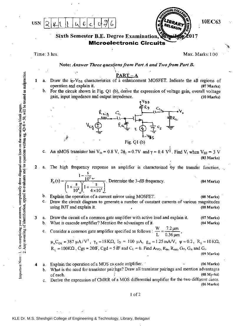
. 10EC63
Time: 3 hrs. Max. Marks: 100
1
2
3
4
Note: Answer Three quest{ons from Part A and Two from Part B.
\.
PA,RT-:--A a. Draw the io-Vos characteristics of a enhai1cement MOSFET. Indicate the all regions of
operation and explain it. (07 Marks)
b. For the circuit shown in Fig. Q 1 (b ), derive the expression of voltage gain, overall voltage
gain, input impedance and output impedence. (10 Marks)
~v,
l CS 7 -;:,
. '"""ss Fig. Ql (b)
I
c. An nMOS transistor has V10 = 0.8 V, 2$r = 0.7V and y = 0.4 V2. Find V1 when Vs8 = 3 V
(03 Marks)
I • '
a. The high frequency response an amplifier is characterized 1by the transfer function,
1--s-105....... . .
FH(s) =...,,(--s....,.)_,,(,-=--=--. -s-,....
1. Determme the 3-dB frequency.
1+- 1+---104 4 x 10⁵
.
""
(04 Marks)
b. Explain the operation of a current mirror using MOSFET. (08 Marks)
c. Draw the circuit diagram to generate_ a number of constant currents of various magnitudes
using BIT and explain it. (08 Marks)
a. Draw the circuit of a common gate amplifier with active load and explain it.
b. What is cascade amplifier? Mention the advantages of it.
c. Consider a common gate amplifier specified as follows: W = 7
·2
µm , L 0.36µm
(07 Marks)
(04 Marks)
µnCox=387µA/V2
, y0 =l8KQ, Io= 100 ~tA, gm=l.25m.A/V, \j!=0.2, R 5 =10KQ,
RL = lOOKQ, Cgs = 20fF, Cgd = 5 ff and CL= 0. Find Avo, Rin, Rout, Gv, Gis and Gi.
(09 Marks)
a. Explain the operation of a MOS ca.1cade a11Ip:tifier. ·· - (06 Marks)
b. What is the need for transistor pair )ngs? Draw all transistor pairings and mention advantages
of each. I (08 Mrrks)
Derive the expression of CMRR of a MOS differential amplifier for the two different .::~scs. (06 Marks)
c.
I of2
~-.
KLE Dr. M.S. Sheshgiri College of Engineering & Technology, Library, Belagavi

~ :· l1. v .. ?, ....
10EC63
••• PART-B
5 a. Explain the operation of a active loaded MOS differential pair. (08 Marks)
b. Why differential amplifiers are well suited for IC fabrication? . .(04 Marks)
c. W_ith neat circuit diagram, explain the operation of two-stage CMOS op-amp crrcmt. ~ ~8Ma~~
·.•
\-- \,,
(1 a. With a mathematical analysis, explain the effect of negative feedback on gain desensitivity
and bandwidth extension. (08 Marks)
b. Draw the structure· of ;-""~erie1s.:.shunt feedback amplifier and derive the expression of input
and output impedance with feedback. (08 Marks)
c. - Draw the Root locus diagram for an amplifier with three pofos and explain it. (04 Marks)
7 a. For the circuit shown in Fig. Q7 (a), determine the values of Vi, i1, ii, Vo and iL. Also
determine the voltage gain Vo , current gain i.L and Power g~in Po . (07 Marks)
~ 11 ~
i2 \0¥-..JL ~ R.,\-7
Fig. Q7 (a)
b. Derive the output voltage expression of a logarithmic amplifier with temperature
com!1Pnsnt10n (09 Marks)
c. With the; help of waveform, explain the effect of slew rate limiting on output sinusoidal
waveform. (04 Marks)
8 a. Define the following performance parameter of a logic circuit family and also draw the
propagation delay and switching times waveform of the logic inverter.
(i) · Noise margin
(ii) Propagation delay.
(iii) Robustness.
(iv) Delay-power product. _ (10 Marks)
b. Implement the following expressions,using AOI gates and also write logic equivalent circuit:
(i) F =(A+ B)(C + D)
( ii) F=XY +Z (10 Marks)
** * * * .~
2 of 2 KLE Dr. M.S. Sheshgiri College of Engineering & Technology, Library, Belagavi
USN I I I I I I I I I I I 10EC64
Sixth Semester B.E. Degree Examination, June/July 2017
Antenna and Propagation
Time: 3 hrs. Max. Marks: 100
1
2
3
4
5
Note: Answer FIVE full questions, selecting
at least TWO questions from each part.
PART-A a. Define the term directivity and effective aperture of an antenna. Derive the relation for D in
terms of Ae. (08 Marks)
b. Define the following parameters of antenna: i) Beam area
ii) Radiation pattern
c. An antenna has a field pattern given by E(8) = cos 8 cos 28
i) The half-power beam width ii) The beam width between first nulls.
(08 Marks)
for O ~ 8 ~ 90°. Find:
(04 Marks)
a. State and prove the power theorem and explain its application to an isotropic source. (04 Marks)
b. The radiation intensity of an antenna is given by U = Um sin 2 8 for O ~ 8 ~ n I 2 and
0 ~ ~ ~ 2n. Find the directivity. (04 Marks)
c. Explain field and phase pattern. (05 Marks)
d. Derive an expression for total field in case of two isotropic points with same amplitude and
phase. Plot the relative field pattern when these two isotropic sources are spaced '}J2 apart. (07 Marks)
a. Derive the expression for the radiation resistance of short dipole. (08 Marks)
b. Show that the radiation resistance of a linear "A/2 antenna with sinusoidal current distribution
is equal to 73Q. (08 Marks)
c. For a short dipole "A/15 long, find the efficiency, radiation resistance if loss resistance is In.
Find also the effective aperture. (04 Marks)
a. Derive Far field expressions for small loop antenna.
b. State and explain Babinet's principle.
c. Write notes on patch antenna with applications.
PART-B
(08 Marks)
(06 Marks)
(06 Marks)
a. Explain the Yagi-Uda array antenna. (08 Marks)
b. Explain the working of log periodic antenna. (08 Marks)
c. A 16-turn helical beam antenna has a circumference of "A and turn spacing of 11,/4. What is
(i) HPBW, (ii) Axial ratio, (iii) Gain? (04 Marks)
6 Write short notes on: a. Sleeve antenna
b. Antennas for ground penetrating radars (GPR) c. Ultra wide band antennas d. Plasma antenna
I of 2
(05 Marks)
(05 Marks)
(05 Marks)
(05 Marks)
KLE Dr. M.S. Sheshgiri College of Engineering & Technology, Library, Belagavi

10EC64
7 a. Find the approximate formula for the filed strength in VHF propagation and explain how it varies sinusoidally. (10 Marks)
b. Explain about the diffraction with two basic models. (06 Marks)
c. A VHF communication is to be established at 90 MHz, with the transmitter power of 35
watts. Calculate the LOS communication distance, if the heights of transmitter and receiver
antennas are 40 m and 25 m respectively. (04 Marks)
8 a. Derive the expression for refractive index of an ionospheric layer. (10 Marks)
b. Explain the effects of earth's magnetic field. (06 Marks)
c. A HF radio link is established for a range of 2000 km. If the reflection region of the
ionosphere is at a height of 200 km and has a critical frequency of 6 MHz. Calculate MUF. (04Marks)
* * * * *
2 of2
KLE Dr. M.S. Sheshgiri College of Engineering & Technology, Library, Belagavi

USN I I I I I I I I I I I
Time: 3 hrs.
1 a. b.
2 a. b.
3 a. b.
Note: Answer any FIVE full questions, selecting
at/east TWO questions from each part.
PART-A
Explain the batch processing system with advantages and disadvantages. Explain the goals and functions of operating system.
Explain the differences between monolithic and layered based design. Explain micro kernel based operating system.
Explain programmers view and operating system view of processes. Explain the difference between the threads and processes.
10EC65
Max. Marks:100
(10 Marks)
(10 Marks)
(10 Marks)
(10 Marks)
(10 Marks)
(10 Marks)
4 a. Explain the difference between contiguous and non contiguous memory allocation. (10 Marks)
b. Explain kernel memory allocation. (10 Marks)
PART-B
5 a. Explain virtual memory using paging. b. Explain page replacement policies.
6 a. Explain over view of input/output organization. b. Explain allocation of disk place.
7 a. Describe the real time scheduling. b. Explain process scheduling in UNIX.
8 a. Explain message passing with example.
b. Describe various interprocess communication schemes with UNIX example.
* * * * *
(10 Marks)
(10 Marks)
(10 Marks)
(10 Marks)
(10 Marks)
(10 Marks)
(10 Marks)
(10 Marks)
KLE Dr. M.S. Sheshgiri College of Engineering & Technology, Library, Belagavi

KLE Dr. M.S. Sheshgiri College of Engineering & Technology, Library, Belagavi
!! 0
z ~ t 0 0..
..§
USN I I I I I I I I I I I 10EC664
Sixth Semester B.E. Degree Examination, June/July 2017
Low Power VLSI Design
Time: 3 hrs. Max. Marks: I 00
1
2
3
4
5
6
7
8
Note: Answer FIVE full questions, selecting at least TWO questions from each part.
PART-A
a. What are the different sources of power dissipation?
b. Explain the energy band diagrams of MIS-structure at different bias conditions.
c. Explain briefly long channel MOSFET.
a. Derive and show that expression for short circuit dissipation is given by,
13( )3"C Psc =- Yoo - VT -12 T
b. Explain the charge sharing phenomenon is dynamic circuits.
(04 Marks)
(12 Marks)
(04 Marks)
(12 Marks)
(08 Marks)
a. Explain the conceptual level diagrams of possible improvement
various levels.
is power dissipation at
b. Derive the first order differences algorithm for a discrete LTI-FIR system.
(08 Marks)
(06 Marks)
(06 Marks) c. Explain the data flow graph of FIR filter.
a. Explain the power optimization using operation reduction techniques. (06 Marks)
b. Explain FSM and combinational logic synthesis with suitable state machine representation. (06 Marks)
c. Using Shannon's expansion principle, explain the precomputation of adder-comparator
a.
b.
c.
a.
b.
a.
b.
c.
a.
b.
circuit. (08 Marks)
PART-B
Explain the ratio-logic using only nMOS and pseudo nMOS logic network. (08 Marks)
Realize and implement NANO/ AND logic and XOR/XNOR logic using CPL logic. (06 Marks)
What are the factors influencing leake current in deep submicrometer transistor? (06 Marks)
Explain the low voltage design techniques with respect to reverse Vgs, steeper sub threshold
swing and multiple thresholds. (10 Marks)
Explain the importance of multiple supply voltages and multiple threshold techniques.
Design NANO gate using adiabatic switching for reversible logic.
Explain energy recovery SRAM-core organization.
Explain briefly supply clock generation technique.
Explain various factors essential for software power estimation.
Explain the software power estimation with suitable example.
* * * * *
(10 Marks)
(IO Marks)
(06 Marks)
(04 Marks)
(10 Marks)
(10 Marks)
KLE Dr. M.S. Sheshgiri College of Engineering & Technology, Library, Belagavi
KLE Dr. M.S. Sheshgiri College of Engineering & Technology, Library, Belagavi

E 0
z ~ t: 0
.§
USN I I I I I I I I I I I 10EC665
Sixth Semester B.E. Degree Examination, June/July 2017
Programming in C++
Time: 3 hrs. Max. Marks: I 00
1
2
3
4
5
6
Note: Answer FIVE full questions, selecting
at least TWO questions from each part.
PART-A a. What is preprocessor directive? Explain available preprocessor directives in C++ with
necessary example. (08 Marks)
b. What are the advantages of dynamic allocation of arrays? Explain dynamic allocation
operators with example. (06 Marks)
c. Define object oriented design. Explain, what are the basic features of object oriented design. (06 Marks)
a. Explain following operations:
i) Constant ii) Reference type iii) Enumeration
iv) Namespace v) Typedef vi) Conditional operator (12 Marks)
b. Justify with program how two strings initialized, concatenated, and find the length of the
concatenated string. (04 Marks)
c. Explain vector initialization operations. (04 Marks)
a. Explain basic bitwise operators of C++ with each example.
b. Explain execution operation of continue, break and goto statements. c. Write a C++ program to sort the array of 'n' numbers in ascending order.
(06 Marks)
(06 Marks)
(08 Marks)
a. With a programming example, explain the 'call-by-value' and 'call-by-reference' parameter
passing methods to a function, define function prototype. (08 Marks)
b. Write a C++ program to pass array of IO integer numbers to the user defined function, to
find the largest of the array and return to the calling program, and display the largest value in main( ). (06 Marks)
c. Define inline function. With example, explain inline function. What are its limitations? (06 Marks)
PART-B a. Define exception. What are the advantages of exception? Explain try, catch, throw exception
handling mechanism. (08 Marks)
b. Explain C++ exception features available, catch all, terminate, unexpected. (12 Marks)
a. Create a class with STUDENT, declare data members as: student name, USN, department,
semester, six subject marks. Declare member functions to read( ) and display( ). Calculate
the percentage of a student using percent( ). According to percentage assign class to a
student using result( ), with following condition, if percentage is
i) Above 70% - FCD
ii) Between 60% to 69% - FC
iii) Between 50% to 59% - SC
iv) Below 50% - FAIL
in main program. Make this record for IO students.
b. Explain with example function overloading for constructor operation. I of 2
(12 Marks)
(08 Marks)
KLE Dr. M.S. Sheshgiri College of Engineering & Technology, Library, Belagavi

10EC665
7 a. What is operator overloading? Give general syntax of operator overloading. (04 Marks)
b. In C++, justify with programming example how prefix and postfix increment operator
overloading distinguished. (06 Marks)
c. Write a C++ program to illustrate how the binary '+' operator overloaded for addition of two
complex numbers using friend function operator overloading. (10 Marks)
8 a. Define virtual member. Explain virtual function access with derived class. (06 Marks)
b. Explain multiple inheritance with constructor and destructor operation executed with example. (06 Marks)
c. Explain with example private, public, protected base class inheritance operation for atleast one level. (08 Marks)
*****
2 of2
KLE Dr. M.S. Sheshgiri College of Engineering & Technology, Library, Belagavi

.., 0 z c co t 0 0.
.§
USN I I I I I I I I I I I Seventh Semester B.E. Degree Examination, June/July 2017
Computer Communication Networks
Time: 3 hrs. Max. Marks: 100
1
2
3
4
5
Note: Answer FIVE full questions, selecting
at least TWO questions from each part.
PART-A
a. Explain the ISO-OSI reference model with a neat diagram.
layer.
Discuss the function of each
b. Explain the signaling system seven (SS7) protocol with a neat diagram.
c. Match the following functions to the appropriate layers in the OSI model:
i) Interface to the transmission media.
ii) Dividing the transmitted bit stream into frames
iii) Route determination
iv) Reliable process to process message delivery
v) Format and code conversion services
a. Explain the bit stuffing and unstuffing by taking a suitable example.
b. Explain the configuration modes of HDLC protocol with neat diagrams.
c. Explain the ~top and wa•-t protocol with n~at diagram.
(JO Marks)
(05 Marks)
(05 Marks)
(05 Marks)
(05 Marks)
(JO Marks)
a. Explain the procedure for pure aloha protocol with a neat diagram.
b. A slotted aloha network transmits 200 bit frames using a shared
bandwidth. Find the throughput, if the system produces,
(06 Marks)
channel of 200 kbps
i) 1000 frames per second
ii) 500 frames per second
iii) 250 frames per second
c. Explain the working of CSMA/CD with a neat diagram. (06 Marks)
(08 Marks)
a. Compare the data rates for standard Ethernet, fast Ethernet, gigabit Ethernet and ten gigabit
Ethernet. (04 Marks)
b. Identify whether the following Mac addresses are unicast, multicast or broad cast. i) 4A:30: 10:21: 10: lA
ii) 47: 20: lB: 2E: 08 : EE
iii) FF : FF : FF : FF : FF : FF (06 Marks)
c. What are the common standard Ethernet implementation? Explain with neat diagrams.
PART-8
a. Explain each of the following in brief:
i) Passive hub
ii) Repeater
iii) Bridge
iv) Router
v) Gateway
b. Explaineachofthe following in brief:
i) Bus backbone nct\\"orks
ii) Star backbone net\\·orks
c. What is \·Ian? Explain.
I of2
(10 Marks)
(10 Marks)
(06 Marks)
(04 !\'larks)
KLE Dr. M.S. Sheshgiri College of Engineering & Technology, Library, Belagavi

10EC/TE71 ·•· • .f
6 a. Explair(th.~.'Jl?\!4 datagram format with a neat diagram. (IO Marks)
7
8
b. Explain the classful addressing schemes. (06 Marks)
c. A block of addresses is granted to an organization. If the IP address of one of the host is
205.16.37.39/28, find the first address and last address in the block. (04 Marks)
a. What is the difference between a direct delivery and indirect delivery?
b. What is multicasting? Explain with a neat diagram and mention the
multicasting.
c. Classify the four types of links defined by OSPF and explain.
a. Explain the TCP segment format with a neat diagram.
b. What are the three domains of the domain name space? Explain.
c. How does recursive resolution differ from the iterative resolution?
* * * * *
2 of2
(04 Marks)
applications of
(08 Marks)
(08 Marks)
(10 Marks)
(06 Marks)
(04 Marks)
KLE Dr. M.S. Sheshgiri College of Engineering & Technology, Library, Belagavi

0)
0 z i:: ~ 0 0..
§
USN I I I I I I I I I I I
Time: 3 hrs.
Optical Fiber Communication
Note: Answer FTVE full questions, selecting at least TWO questions from each part.
PART-A
10EC72
Max. Marks: 100
1 a. Summarize the inherent advantages of optical fiber over conventional copper cables. (06 Marks)
b. Describe with neat diagram different types of optical fiber waveguides. Using ray theory, explain the propagation oflight inside the fiber. (08 Marks)
c. A silica optical fiber with a core diameter large enough to be considered by ray theory analysis has a core refractive index of 1.5. A light ray is incidented at the core-cladding interface with a critical angle of 78. 5 °. Estimate: i) Refractive index of cladding ii) Numerical aperture iii) Th1 acceptance angle in air for the fiber (06 Marks)
2 a. Illustrate the different types of scattering losses in optical fiber with suitable equations. (08 Mark~)
b. Explain what is meant by the critical bending radius for an optical fiber. Write equation of critical radius of curvature for multimode and single mode fibers. (06 Marks)
c. A multimode fiber with a core refractive index of 1.5, a relative refractive index difference
of 3% and an operating wavelength of 0.82 µm. Estimate the critical radius of curvature at
which large bending losses occur. (06 Marks)
3 a. Draw and explain the cross-sectional view of a typical A.£GaAs double heterojunction LED,
along with the energy diagram. (08 Marks)
b. Sketch and explain the GaAs homojunction injection laser with a Fabry-Perot cavity. (06 Marks)
c. A planar LED is fabricated from'Gallium Arsenide which has a refractive index of 3.6, i) Calculate the optical power emitted into air as a percentage of the internal optical power
for the device when the transmission factor at the crystal-air interface is 0.68.
ii) When the optical power generated internally is 50% of the electric power, determine the
external power efficiency. (06 Marks)
4 a. With the aid of simple sketches, outline optical fiber coupler types and their functions. (08 Marks)
b. Discuss different types of fiber misalignment and the factors which causes the losses due to those misalignment. (06 Marks)
c. A single mode fiber has the following parameters: Normalised frequency (V) = 2.40 Core refractive index (n1) = 1.46
Core diameter (2a) = 8µm Numerical aperture (NA) = 0.1
Normalised spot size (ro) = 3.12 µm.
Estimate the total insertion loss of a fiber joint with a lateral misalignment (Y) of I ~tm and
an angular misalignment (8) of 1 °. (06 '.\larks)
I of2
KLE Dr. M.S. Sheshgiri College of Engineering & Technology, Library, Belagavi

5
6
/.I""'••' '· ..... ~,~
· ... :.-
10EC72
. .. c;..,:;.:;,;-::~>.,' PART - B
a. Briefly explain the quantum limit. (04 Marks)
b. What is a Burst_ Mode receiver? Explain. (06 Marks)
c. Derive the equation for performance fidelity of an analog receiver. Substantiate that for a
large optical signals, signal to noise ratio represents the quantum limit for receiver
sensitivity. (10 Marks)
a. With a diagram, briefly explain the operation of multichannel amplitude modulation. (08 Marks)
b. Explain the radio frequency over fiber concept of a broadband wireless access network for interconnecting antenna base stations with the central controlling office. (08 Marks)
c. In a multimode link using LED as optical source, material dispersion related rise time degradation is 21 ns over the 6 km link. Receiver has a 25 MHz bandwidth. Fiber has
500 MHz.km bandwidth-distance product with mode mixing parameter, q = 0.7. Assuming
LED with drive circuit has rise time of 15 ns, modal-dispersion-induced fiber rise time is 3.9
ns and the contribution to the rise-time degradation from the receiver is 14 ns. Calculate link
rise time. (04 Marks)
7 a. Describe the operational principles of WDM, depicting the implementation of a typical
8
WDM network containing various types of optical amplifier. (08 Marks)
b. With a neat diagram, explain the working principle of Mach-Zehnder inter-ferometer
multiplexer. (08 Marks)
c. The input wavelengths of a 2 x 2 silicon Mach-Zehnder inter ferometer are separated by
10 GHz. The effective refractive index in the waveguide is 1.5. Calculate waveguide length
difference. (04 Marks)
a. Explain with the aid of neat diagram, three possible EDFA configurations.
b. Describe:
i) SONET/SDH frame format ii) SONET/SDH rings
c. An EDFA is pumped at 980 nm with a 30 mW pump power. If the gain at
20 dB, calculate maximum input power.
* * * * *
2 of2
0
(06 Marks)
(10 Marks)
1550 nm is
(04 Marks)
KLE Dr. M.S. Sheshgiri College of Engineering & Technology, Library, Belagavi

<)
0 z
~ 0 0..
.§
USN I I I I I I I I I I I 10EC73
Seventh Semester B.E. Degree Examination, June
Power Electronics
Time: 3 hrs. Max. Marks: 100
1
2
3
4
Note: Answer FIVE full questions, selecting at least TWO questions from each part.
PART-A
a. Draw the control characteristics of SCR, GTO and MCT with circuit diagrams and waveforms of control signal and output voltage. (09 Marks)
b. What is Schottky diode? Mention its advantages. (04 Marks)
c. What are the peripheral effects of power electronic equipment and mention remedies of its. (07 Marks)
a. Explain the following parameters with respect to switching limits:
(i) Second breakdown (SB).
(ii) Forward-biased safe operating area.
(iii) Power derating.
(iv) Breakdown voltages.
b. Explain proportional and antisaturation control of a base drive.
(12 Marks)
(08 Marks)
a. For the circuit shown in Fig. Q3 (a) obtain the minimum gate pulse width is required for
reliable triggering of the SCR if gated at 2: angle in every +ve half cycle. Assume 3
Vs = 325 sin 3 l 4t and latching current of 15 mA.
Fig. Q3 (a)
R.~\C)JL
L-:::0,\\-\
b. Explain the operation of a full wave RC-firing circuit with waveforms.
Explain how thyristors are protected against high di. dt
c.
(06 Marks)
(08 Marks)
(06 Marks)
a. For the circuit shown in Fig. Q4 (a), find the average load voltage and current if the load
resistance is 10 n and firing angle is 45°. Assume supply of 230 V, 50 Hz. (06 Marks)
E:
Fig. Q4 (a)
b. Explain the operation of single phase semiconverter with circuit and waveforms. Derive the
expression for the average and rms value of the output voltage. (Assume RL-load). (10 Marks)
c. What are the advantages of circulating current mode dual converter? (04 Marks)
1 of2
KLE Dr. M.S. Sheshgiri College of Engineering & Technology, Library, Belagavi

10EC73
PART-B
5 a. Explain the operation of a self commutation by resonating load and also derive the
expression of i(t) = V8Jf sin( let). (12 Marks)
b. For the circuit shown in Fig. Q5 (b) the current through R1 and R2 is 25 A and tum off time
of both SCR's is 40 µsec. Find the value of capacitor for successful commutation. (04 Marks)
Fig. Q5 (b) c. Compare natural and forced commutation. (04 Marks)
6 a. Explain the operation of a single phase Bi-directional controller with resistive load. Derive
the expression of RMS value of the output voltage. (10 Marks)
b. A single phase AC voltage controller shown in Fig. Q6 (b) has a resistive load of 10 Q and
input voltage of 120 V, 60 Hz. The delay angle of thyristor T1 is 1t. Determine 2
(i) RMS value of the output voltage.
(ii) Input power factor.
(iii) Average input current. (07 Marks)
Fig. Q6 (b)
c. Mention the applications of AC voltage controllers. (03 Marks)
7 a. Explain the working principles of step down chopper with RL-load. Derive the expression of
peak-peak ripple in the load current. (14 Marks)
b. A step up chopper has input voltage of 220 V and output voltage of 660 V. If the
non-conducting time of thyristor chopper is 100 µsec. Compute the pulse width of the output
voltage. (conduction period). (06 Marks)
8 a. Explain the following performance parameters of a inverters:
(i) Harmonic factor of nth harmonic.
(ii) Total harmonic distortion. (iii) Distortion factor.
b. Explain the operation of single phase bridge inverters.
c. What is inverter? Mention applications of it.
* * * * *
2 of2
(06 Marks)
(10 Marks)
(04 Marks)
KLE Dr. M.S. Sheshgiri College of Engineering & Technology, Library, Belagavi

(\)
0 z E ~ 0
§
USN I I I I I I I I I I I
Seventh Semester B.E. Degree Examination, June/July 2017
Embedded System Design
10EC74
Time: 3 hrs. Max. Marks:100 Note: Answer FIVE full questions, selecting
at least TWO questions from each part.
PART-A
1 a. What is an embedded system? Explain briefly the various components in a microprocessor
based embedded system with a block diagram. (10 Marks)
b. What are the considerations and important steps in developing an embedded system? Briefly describe the major elements of the embedded system development life cycle. (10 Marks)
2 a. Explain the block diagram of a special purpose microprocessor. (06 Marks)
b. Compare: (i) Harvard and Von-Neumann architecture. (ii) Big Endian and Little Endian formats. (iii) RISC and CISC registers. (06 Marks)
c. Write the block diagram ofRTN for a microprocessor Datapath and memory interface. Also explain instruction cycle steps with ISA level instructions. (08 Marks)
3 a. Write the inside and outside diagrams for SRAM along with read and write operations. (08 Marks)
b. Explain an associative mapping cache implementation. (06 Marks)
c. Explain dynamic memory allocation with its schemes. (06 Marks)
4 a. What is product life cycle? Briefly explain waterfall, V cycle, spiral life cycle models. (10 Marks)
b. What are the general software design steps? Write a hardware architecture and data and counter flow diagram of a counter system and explain briefly flow diagram. (10 Marks)
PART-B
5 a. What is a thread? Explain the different types of threads used in operating system. (06 Marks)
b. Describe:
(i) Reentrant/Non Reentrant code. (ii) Foreground I Back ground system.
(iii) Pre-emptive scheduling. (06 Marks)
c. How the information is stored in stack frame? Also explain the different types of stacks used in the memory management. (08 Marks)
6 a. Define an embedded operating system with specific functions. Also explain Kernel with the various types of services. (08 Marks)
b. Design a simple operating system Kernel with a suitable code. (08 Marks)
c. What is a Task control block? What are the major components of the TCB? (04 Marks)
l of2
KLE Dr. M.S. Sheshgiri College of Engineering & Technology, Library, Belagavi
10EC74
7 a. . Wh~t is .time loading? Describe the methods by which we can perform a time loading
analysis of an embedded application. Discuss the advantages and disadvantages of each. (10 Marks)
b. Explain Big-0 notation and Big-0 arithmetic used for comparing algorithms. (10 Marks)
8 a. Write a short notes on the following:
(i) Performance optimization.
(ii) Tricks of the trade. (10 Marks)
b. Analyse the following two types of loop and determine the number of iterations to be
performed and the number of steps per iteration.
(i) loop 1
int sum= 0; For (int j = O; j < N; j++)
Sum= Sum+ j;
(ii) loop 2
int sum= 0;
for (int j = O; j < 100; j++) Sum = Sum+ j ; (10 Marks)
* * * * *
2 of2
KLE Dr. M.S. Sheshgiri College of Engineering & Technology, Library, Belagavi

(!}
0 z
I 0..
.§
\
USN I I I I I I I I I I I 10EC751
Seventh Semester B.E. Degree Examination, June/July 2017
Time: 3 hrs.
DSP Algorithms and Architecture
Note: Answer FIVE full questions, selecting at least TWO questions from each part.
PART-A
Max. Marks: 100
1 a. Explain the major architectural features of programmable Digital Signal Processing devices. (08 Marks)
b. With the help of block diagram explain the digital filter. (04 Marks)
c. An FIR filter is described by differential equation. y(n) = 0.6 x(n) + 0.6 x(n - 1). Determine
system function, frequency response, impulse response, magnitude response function and phase response. (08 Marks)
2 a. Draw the structure of 4 x 4 Braun multiplier and explain its operation. (08 Marks)
b. Describe the implementation of single MAC unit for an 8-tap (coefficient) FIR filter. (08 Marks)
c. Find the total time required to compute the sum of 250 products using pipelined MAC unit. The MAC unit execution time is 100 nsec. (04 Marks)
3 a. What is meant by addressing mode? Explain absolute, accumulator and direct addressing modes ofTMS 320C54xx processor. (08 Marks)
b. Describe the operations of the following :
i) MPY *AR2 - , * AR4 + 0, B ii) MAC * AR3 - , * AR4 +, B, A
iii) MAS * AR3 -, * AR4 + B, A (06 Marks)
c. Explain the hardware timer ofTMS 320 C54xx DSP with logical block diagram. (06 Marks)
4 a. What are the different types of serial I/0 ports in C54xx? Explain the application of each serial I/0 port. (08 Marks)
b. With a neat diagram, describe the different stages of pipelining in C54xx processors. (08 Marks)
c. Write a TMS 320C54 xx ALP o find a sum of a set of 4 numbers stored in on array labeled
'num'. (04 Marks)
PART-B
5 a. What is the significance of Q-notation in DSP? (04 Marks)
b. Explain the IV1h order FIR filter implementation with the organization of samples and filter
coefficients in circular buffer. (10 Marks)
c. What is interpolation? Explain the interpolation process to implement interpolation filter with interpolation factor 'L'. (06 Marks)
1 of2
KLE Dr. M.S. Sheshgiri College of Engineering & Technology, Library, Belagavi

6 a. Determine the following for 128 point FFT computation. i) Number of stages ii) Number of butterflies in each stags iii) Number of butterflies needed for the entire computation
10EC751
iv) Number of butterflies that need on multiplication. (04 Marks)
b. Explain how the bit reversed index generation can be done in an 8-point DFT computation. (06 Marks)
c. What is the need for scaling of inputs? Derive the scaling required in FFT calculation. (10 Marks)
7 a. Design a data memory system with the address range 000800h - OOOFFFh for a C5416 processor. Use 2Kx8 SRAM memory chips. (10 Marks)
b. What are the features ofDMA in C54xx processor? (04 Marks)
c. Explain register sub-addressing technique for configuring DMA. (06 Marks)
8 a. With a neat block diagram, explain the synchronous serial interface (SSI) between C54xx and CODEC device. (10 Marks)
b. With a neat block diagram, explain the DSP based biotelemetry receiver system. (10 Marks)
* * * * *
2 of2
KLE Dr. M.S. Sheshgiri College of Engineering & Technology, Library, Belagavi

Seventh Semester B.E. Degree Examination,
Real Time Systems
OEC/TE762
Time: 3 hrs. Max. Marks: 100
1
2
3
4
5
6
Note: Answer any FIVE full questions, selecting
at/east TWO questions from each part.
PART-A
a. Give two definitions for real time system. b. With a neat diagram, explain computer control system showing hardware
interface.
c. Explain with block diagram sampled feedback control system.
a. Explain continuous processing and laboratory system.
b. Draw and explain Direct Digital Control (DDC) c. What are advantages of DOC over analog control?
a. Explain functions ofISR with the help of flow chart. b. Explain SIMD and MISD with neat diagram. c. Mention features of specialized processors.
(04 Marks)
and software (08 Marks)
(08 Marks)
(08 Marks)
(08 Marks)
(04 Marks)
(08 Marks)
(08 l\'larks)
(04 Marks)
a. Define CUTLASS. What are the major requirements of CUTLASS? Describe CUTLASS host target configuration. (10 Marks)
b. What are the basic langua 0e requirements for RTS la!1guage along with basic language features? (10 Marks)
PART-B
a. Explain with neat diagram structure of RTOS. b. Draw and explain task state diagram.
c. Explain cyclic and preemptive scheduling strategies.
a. Explain detailed arrangement of10SS.
b. Explain serially reusable code and re-entrant code. c. Write a note on Liveness ofRTS.
(08 Marks)
(08 Marks)
(04 Marks)
(08 Marks)
(08 Marks)
(04 Marks)
7 a. Write a sample program to transfer of controller parameters using semaphores.
b. Explain with the help of flowchart mutual exclusion using conditional flags.
(10 Marks)
(10 Marks)
8 a. Explain the outline of abstract modeling approach of ward and Mellor. b. Explain software modeling with neat diagram.
c. Compare Ward and Mellor with Hatley and Pirbhai.
* * * * *
(08 Marks)
(081\farks)
(04 Marks)
KLE Dr. M.S. Sheshgiri College of Engineering & Technology, Library, Belagavi

j,.,. ">'
,,.; •• !"
KLE Dr. M.S. Sheshgiri College of Engineering & Technology, Library, Belagavi
~ 0
z
~ 0
.§
USN I I I I I I I I I I I .~ ..•.. •
Seventh Semester B.E. Degree Examination, June/July 2017
Digital Image Processing
Time: 3 hrs. Max. Marks: 100
1
2
3
4
Note: Answer any FIVE full questions, selecting at/east TWO questions from each part.
PART-A
a. Explain the fundamental steps in digital image processing.
b. Explain mass storage capability in image processing applications and also
categories.
c. Write a note on optical illusions.
(08 Marks)
its principal
(07 Marks)
(05 Marks)
a. Consider the two image subsets s1 and s2 shown in Fig. Q2(a). For v = {l}, determine
b.
c.
whether these two subsets are : i) 4-adjacent ii) 8-adjacent iii) m-adjacent. (06 Marks)
S" g 2..-\ -~-,- - - - - - ,----c, Q o O O \ 0 0 \ l O
\\o o \ 010 oo'\ \ I O o \ O i \ a o j (j
oo: __ oo -' --' - ~L°-- ~ c, a_J D \ \ \ C) () ,-, \
Fig.Q2(a)
Explain the process of generating digital image.
Explain linear and non-linear operations in digital image processing.
(08 Marks)
(06 Marks)
a. Define ID-unitary transform, and mention its properties. (06 Marks)
b. Compute 20-DFT of a 4 x 4 grey scale image shown in Fig.Q3(a) and corresponding
inverse DFT. (08 Marks)
1 1 1 1
1 1 1 1 V=
1 1 1 1
1 1 1 1
Fig.3Q(b)
c. Prove that FF* T = 1, where F is the DFT matrix. (06 Marks)
a. Write the generation of N x N Hadamard transform matrix by iterative rule. Mention its
advantages and properties. (08 Marks)
b. What are the properties of slant transform and also find forward slant transform and inverse
slant transform of U.
1
1 Where U =
1
1
(06 Marks)
c. Define I-Dimensional DCT for N = 4 obtain N x N cosine transform matrix(c). (06 Marks)
1 of2
KLE Dr. M.S. Sheshgiri College of Engineering & Technology, Library, Belagavi
5 a. b.
c. d.
6 a.
b.
c.
7 a. b.
8 a.
b.
c.
PART-B
Explain the following terms with respect to image enhancement. Log transformation Bit-plane slicing Histogram equalization Image averaging.
10EC763
(20 Marks)
Draw the block diagram of a homomorphic filtering approach for image enhancement and explain it. (08 Marks)
Explain Butterworth lowpass filter for smoothing. (06 Marks)
Discuss high Boost filtering for sharpening. (06 Marks)
Discuss the important noise probability density functions. (10 Marks)
Discuss the various mean filters for restoration in the presence of noise only-spatial filtering. (10 Marks)
Explain the color characteristics to distinguish between vanous colors. Write the
trichromatic coefficients interms ofX, Y and Z. Draw the block diagram of a gray level to color transformations and explain it.
Write a note on CMY color model.
* * * * *
2 of2
(08 Marks)
(08 Marks)
(04 Marks)
KLE Dr. M.S. Sheshgiri College of Engineering & Technology, Library, Belagavi

<)
0 :z E o:l t:: 0 0..
.§
USN I I I I I I I I I I I 10EC81
Eighth Semester B.E. Degree Examination, June/July 2017
Wireless Communications
Time: 3 hrs. Max. Marks: 100
Note: Answer any FIVE full questions, selecting atleast TWO questions from each part.
PART-A
1 a. Briefly explain the different generation of cellular system. (10 Marks)
(10 Marks) b. Explain with a neat flow diagram AMPS mobile originated call.
2 a. Explain with diagram mobile switching centre (MSC). (10 Marks)
b. Explain with necessary diagram the formats of cell global identity number, mobile global
identity number, IMEI number and local area identity number. (10 Marks)
3 a. Explain differences between cell splitting and cell sectoring capacity expansion techniques
with neat diagram. (07 Marks)
b. For a mobile system of cluster size of 12 determine the frequency reuse distance if the cell
radius is 8 km. (03 Marks)
c. Name three basic functions performed by the location management and explain cellular
location updating with figure. (1 o Marks)
4 a. Explain with diagram GSM network architecture. (10 Marks)
b. Explain in detail GSM channel concepts. (10 Marks)
PART-B
5 a. Explain with flow diagram GSM call configuration and call accepted. (10 Marks)
b. Explain with diagram GSM intra BSC handover operation. (10 Marks)
6 a. Explain reverse traffic channel generation in CDMA. (10 Marks)
b. Explain different call hand offs in CDMA system. (10 Marks)
7 a. What is the received power dBm for a signal in free space with a transmitting power of
800 mW at a frequency of 980 MHz and distance from the receiver is 6000m, if the
transmitting receiving gain is approximately equal to 1. What is the path loss in dB? (06 Marks)
b. Explain direct sequence and frequency hopping spread spectrum. (08 Marks)
c. Explain RAKE receiver with a diagram. (06 Marks)
8 a. List four fundamental ways in which 802.16a (Wimax), 802.11 in (WLAN) and 802.15 (Bluetooth) different from one another. (04 Marks)
b. Explain Bluetooth protocol stack with diagram. (08 Marks)
c. Explain with suitable diagram independent basic service set networks and distribution
system concept supported by IEEE 802.11 architecture. (08 Marks)
* * * * *
KLE Dr. M.S. Sheshgiri College of Engineering & Technology, Library, Belagavi

KLE Dr. M.S. Sheshgiri College of Engineering & Technology, Library, Belagavi

USN I I I I I I I I I I I 10EC82
Eighth Semester B.E. Degree Examination, June,......&IW1""'
Digital Switching Systems Time: 3 hrs. Max. Marks: 100
1
2
3
4
5
6
7
8
Note: Answer FIVE full questions, selecting
at least TWO questions from each part.
PART-A
a. Write four-wire circuit used in two-way transmission network and explain its working principle. (08 Marks)
b. Explain network topologies in brief (06 Marks)
c. Express the following power levels in dBm and dBW: (i) 1 mW; (ii) 1 W; (iii) 2 mW (06 Marks)
a. Design a 10,000 line step-by-step telephone exchange with a suitable diagram.
b. Enumerate the functions of switching system. c. Explain the operation of BO RSC HT circuit with a suitable block diagram.
(06 Marks)
(08 Marks)
(06 Marks)
a. Derive an expression for second Erlang's distribution formula. (08 Marks)
b. A group of20 trunks provides a grade of service of0.01 when offered 12 E of traffic: (i) How much is the grade of service improved if one extra trunk is added to the group?
(ii) How much does the grade of service deteriorate if one trunk is out of service?
c. A group of five trunks is offered 2E of traffic:
Find (i)
(ii) (iii)
(iv)
The grade of service. The probability that only one trunk is busy. The probability that only one trunk is free.
The probability that at least one trunk is free.
(06 Marks)
(06 Marks)
a. Deduce the expression to determine the total number of cross points for two stage network
with incoming trunks M greater than outgoing trunks N. (06 Marks)
b. Explain progressive, skipped and homogeneous gradings. (06 Marks)
c. Design a three stage network for 100 incoming trunks and 400 outgoing trunks. (08 Marks)
PART-B
a. Explain space-tin1e-space switching network with a suitable block diagram. (07 Marks)
b. Describe the frame alignment and synchronization networks. (07 Marks)
c. Explain cross-bar or space switching with a suitable diagram. (06 Marks)
a. Explain the classification of digital switching system with a suitable block diagram. (10 Marks)
b. Describe the concept of software linkages during a call required in telephony system. (10 Marks)
a. Describe the organizational interfaces of a typical digital switching system control office. (10 Marks)
b. Use strategic analysis and highlight to improve the software quality with a neat block
diagram. (10 Marks)
a. Write a call connection flow-chart and a basic steps necessary to complete a simple call through a digital switching system. (12 Marks)
b. Write short notes on:
(i) Common characteristics of digital switching system. (ii) Analysis report for digital switching system. (08 Marks)
* * * * *
KLE Dr. M.S. Sheshgiri College of Engineering & Technology, Library, Belagavi

KLE Dr. M.S. Sheshgiri College of Engineering & Technology, Library, Belagavi

USN I I I I I I I I I I I 10EC832
Eighth Semester B.E. Degree Examination, June/July 2017
Network Security
Time: 3 hrs. Max. Marks: 100
1
2
3
4
5
6
7
Note: Answer FIVE full questions, selecting
at least TWO questions from each part.
PART-A
a. Define passive and active security attacks. Discuss the functioning of following attacks with diagrams: i) Masquerade ii) Replay iii) Modification of messages iv) Denial of service (10 Marks)
b. With a neat diagram, discuss the functioning of network security model. List four basic tasks
a. b.
c.
a.
b. c.
a. b.
of designing security model. (10 Marks)
Encrypt the plain text "HELLO" using the play fair cipher with the key "EXAM". (08 Marks)
Explain the operation of Caeser cipher with an algorithm. Derive the cipher text using Caeser Cipher for the following plain text message with key length K = 3, "logic". (06 Marks)
Explain the single round of DES-encryption model. (06 Marks)
Explain the RSA algorithm. In a RSA algorithm system it is given that p = 7, q = 11, e = 17 and M = 8. Find the cipher text "c" and decrypt "c" to set plain text M. (10 Marks)
Describe the requirements for a Hash function. (05 Marks)
Explain Diffie Hellman key exchange algorithm with example. (05 Marks)
With neat diagram, explain digital signature algorithm (DSA). List and explain the general approach to deal with replay attacks.
PART-B
(10 Marks)
(10 Marks)
a. Discuss Security Socket Layer (SSL) record protocol in terms of fragmentation, compression and encryption. (10 Marks)
b. Describe the sequence of events that are required for a transaction in Secure Electronic Transaction (SET). (10 Marks)
a. Briefly describe the three classes of intruder. b. Explain approaches to intrusion detection system. c. Give a detailed account on UNIX password management.
a. Briefly describe the most significant types of virus. b. With a neat diagram, explain digital immune system.
(06 Marks)
(04 Marks)
(10 Marks)
(10 Marks)
(10 Marks)
8 a. Explain the types of firewalls in detail with necessary sketch. (09 Marks)
(06 Marks)
(05 Marks)
b. Explain briefly about the trusted systems. c. Briefly discuss the concept of reference monitor with diagram.
* * * * *
KLE Dr. M.S. Sheshgiri College of Engineering & Technology, Library, Belagavi

KLE Dr. M.S. Sheshgiri College of Engineering & Technology, Library, Belagavi

USN I I I I I I I I I I I 10EC842
Eighth Semester B.E. Degree Examination, J
Real Time Operating Systems
Time: 3 hrs. Max. Marks: 100
1
2
3
4
5
6
Note: Answer FIVE full questions, selecting
atleast TWO questions from each part.
PART-A
a. Write the pseudocode for event driven real time service. (06 Marks)
b. Write the basic block diagram of distributed continuous media real time services. (04 Marks)
c. Explain real time service timeline with hardware acceleration and without hardware acceleration. (10 Marks)
a. What are the 3 resources to be considered for the design of any embedded system? Mention the issues to be considered for these in brief. (10 Marks)
b. Explain how the code for computing the satellite position function can be made thread safe reentrant by using task lock() and task unlock() function. (10 Marks)
a. Derive an equation for RMLUB considering two services with two different cases. (12 Marks)
b. Describe the relationship between sufficient, necessary and N and S feasibility tests using subset diagram. (10 Marks)
a. Explain pipeline stage overlap with a depth of 4, Mention the factors that contribute for of CPI[Clocks Per Instruction] and explain how hazards can be minimized. (10 Marks)
b. Explain WCET and ACET with necessary equations. Explain each and every parameter in the equations. (10 Marks)
PART-B
a. What is pnonty inversion? Mention three conditions
inversion. Explain the solution for priority inversion. b. Explain how to handle missed deadlines.
a. Explain test access ports and power on self test (POST]. b. Explain exceptions and assert with example.
that cause unbounded priority (12 Marks)
(08 Marks)
(10 Marks)
(10 Marks)
7 a. Explain building performance monitoring in to software. b. Explain path length, efficiency and calling frequency.
(10 Marks)
(10 Marks)
8 a. With a simple C code with two paths perform MCDC testing. b. With a neat block diagram, explain the architecture of PIC microcontroller.
* * * * *
(10 Marks)
(10 Marks)
KLE Dr. M.S. Sheshgiri College of Engineering & Technology, Library, Belagavi