Embed Size (px)
Citation preview
This is an electronic reprint of the original article.This reprint may differ from the original in pagination and typographic detail.
Powered by TCPDF (www.tcpdf.org)
This material is protected by copyright and other intellectual property rights, and duplication or sale of all or part of any of the repository collections is not permitted, except that material may be duplicated by you for your research use or educational purposes in electronic or print form. You must obtain permission for any other use. Electronic or print copies may not be offered, whether for sale or otherwise to anyone who is not an authorised user.
Khodaparast, Aryorad ; Hassani, Mohammadjavad; Azimi, Erfan ; Adabi, M. Ebrahim; Adabi,Jafar; Pouresmaeil, EdrisCircuit Configuration and Modulation of a Seven-Level Switched-Capacitor Inverter
Published in:IEEE Transactions on Power Electronics
DOI:10.1109/TPEL.2020.3036351
Published: 06/11/2020
Document VersionPeer reviewed version
Please cite the original version:Khodaparast, A., Hassani, M., Azimi, E., Adabi, M. E., Adabi, J., & Pouresmaeil, E. (2020). Circuit Configurationand Modulation of a Seven-Level Switched-Capacitor Inverter. IEEE Transactions on Power Electronics, 36(6),7087-7096. [9250604]. https://doi.org/10.1109/TPEL.2020.3036351

© 2020 IEEE. This is the author’s version of an article that has been published by IEEE. Personal use of this material is permitted. Permission from IEEE must be obtained for all other uses, in any current or future media, including reprinting/republishing this material for advertising or promotional purposes, creating new collective works, for resale or redistribution to servers or lists, or reuse of any copyrighted component of this work in other works.
1
Abstract—In this paper, a step-up seven-level inverter supplied
by a single DC source suitable for renewable energy application is
presented. Forming the desired output is realized by charging
capacitors and synthesizing them based on switched-capacitor
concept. This structure is praised for the ability of sensor-less
voltage balancing of the capacitors, reducing control complexity to
produce a bipolar staircase waveform. It also benefits from
regenerative performance, avoiding unwanted capacitors
overvoltage. Phase Disposition Pulse Width Modulation (PD-
PWM) technique is utilized to control the circuit operation.
Furthermore, a comparison with other recent topologies reveals
that losses, number of semiconductor devices, and gate driver
circuits are reduced. Theoretical analysis is verified through a
laboratory prototype implementation. Experimental results under
various types of loads approve the performance of the proposed
inverter and validity of the design. Finally, maximum
experimental efficiency of 94.3% (115 V, 250 W load) was reached.
Index Terms—multilevel inverter; single-source; switched-
capacitor; step-up converter; self-balancing.
I. INTRODUCTION
owadays, increasing use of Renewable Energy Sources
(RESs) due to the end of fossil energy and the necessity of
reducing gas emissions have been influencing energy arena.
Mostly these sources generate DC power while the
conventional power systems are in AC form. Hence, for
connecting these energy sources to the power grid, various
types of DC-AC converters are introduced. Among all, Multi-
Level Inverters (MLIs) have significantly drawn the attention
of electrical engineers. These structures are praised for their
better quality of output waveform, lower voltage stresses
(dv/dt), less THD (Total Harmonic Distortion) and their ability
to operate in lower switching frequencies [1]. MLIs have
become popular and have some advantages in many
applications such as fuel cells [2], solar panels [3], electric
vehicles [4], motor drives [5], wind turbines and grid-connected
applications [6-7]. The most applicable structures among them
include Cascaded H Bridges (CHB) [8], Neutral Point Clamped
Manuscript received March 28, 2020; revised August 24, 2020; accepted
October 22, 2020.
A. Khodaparast, M.J. Hassani, E. Azimi, and J. Adabi are with the Faculty
of Electrical and Computer Engineering, Babol Noshirvani University of
Technology, Babol 47148-71167, Iran (e-mail: [email protected]; [email protected]; [email protected]; [email protected]).
(NPC) [9], Flying Capacitor (FC) [10] and Switched Capacitor
(SC) [11].
The CHB topology is famous for its modularity and
simplicity to expand, leading to an increase in the number of
output voltage levels. According to the aforementioned pros, by
increasing H-bridge cells, the number of required switches and
independent DC voltage sources are raised in CHB structures
[12]. In this circumstance, implementation complexity, cost
increment and bulky system caused by low-frequency operation
of the CHB structures increase [13]. To alleviate these
problems, applying asymmetrical DC voltage sources [14] and
a cascaded transformer [15] are proposed. Both NPC and FC
structures suffer from voltage balancing complexity of DC-
Link capacitors. Moreover, high number of semiconductor
components decrease the reliability of the circuit and its
application. Also, among their active switches they don’t have
the ability of equal voltage sharing, both statically and
dynamically [16-17].
Switched-Capacitor Multi-Level Inverters (SCMLIs) are
therefore introduced in order to cover the abovementioned
problems. Many new converters were designed to decrease the
number of components such as semiconductors, DC sources,
and capacitors to lessen costs but they have other drawbacks in
their structure [18-19].
One of the most essential traits for such converters
(especially in many renewable energy applications with low
voltage DC source such as solar systems) which standard MLI
circuits do not possess is boosting capability. The voltage
boosting is realized by charging capacitors and then summing
the capacitors voltages up in a series connection to be applied
to the output, eliminating the need for bulky transformers or
inductors [20-21].
Another crucial character for an SCMLI circuit is whether
the inverter can be used in application with regenerative load
feature or not. For any inverter circuits, every time interval that
the polarity of the output voltage and current are the same, the
power is supplied to the load and the inverter is in “inverting”
mode. Otherwise, the inverter is in “rectification or
regeneration” mode [22]. Application with regenerative loads
M. E. Adabi is a Postdoctoral Researcher with Ecole Centrale de Nantes in
Laboratoire des Sciences du Numériques de Nantes, Nantes, France, (e-mail:
E. Pouresmail is with the department of electrical engineering and
automation (EEA) at Aalto University, Espoo, Finland. (e-mail: [email protected]).
Circuit Configuration and Modulation of a
seven-level Switched-Capacitor Inverter
Aryorad Khodaparast, Mohammadjavad Hassani, Erfan Azimi, M. Ebrahim Adabi, Jafar Adabi, and
Edris Pouresmaeil, Senior Member, IEEE
N
2
require inverters with a bidirectional power flow preventing the
capacitors from over-charging and potential damages. Ergo, the
excess charge is fed to the input source. In this case, [23-26]
introduced new SCMLI structures with regenerative load
feature. Also, they all have the boosting capability except for
[26] where the maximum amplitude of the output is equal to the
input source. Besides, the capacitors’ voltages in [23-25] are
self-balanced and there is no need for any extra balancing
control system. However, the number of components required
for these topologies are high. The structures introduced in [20],
[27-29] can boost the input voltage, but as they use series diodes
in their capacitors’ charging paths, they lack the regenerative
load feature.
This paper presents a seven-level single source step-up boost
inverter with a low number of components. It requires two
capacitors to boost the input voltage up to 3Vin. Phase
Disposition Pulse Width Modulation (PD-PWM) control
strategy is used to produce the desired output waveform with
lower harmonic content. By charging or discharging capacitors
in small sequential time intervals, they would face the least
possible voltage drop. This structure is suitable for a vast range
of low voltage single-source application using photovoltaic,
batteries, and fuel cells (without any need for bulky and
sometimes low efficient inductors).
This study is organized as follows: The working principles of
the proposed circuit are brought in Section II, containing
capacitors charging pattern, different operation modes and a
brief note on circuit modulation method. Section III reveals the
determination of circuit capacitors, power loss calculation and
a comparative discussion of the presented structure against
several recent topologies. Further, design considerations and
results of a test setup including both regenerative and non-
regenerative load behaviors are added in Section IV.
Conclusions are finally represented in Section V.
II. PRINCIPLE OF OPERATION
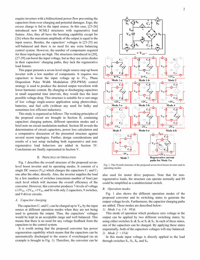
Fig. 1 describes the overall structure of the proposed seven-
level boost inverter and its operating modes. It consists of a
single DC source (Vdc) which charges the capacitors C1 and C2
one after the other, directly. Also, the inverter supplies the load
by a few numbers of switches (maximum number of four) per
each level which will increase the overall efficiency of the
converter. However, this converter produces 7-levels of voltage
(±3Vdc, ±2Vdc, ±1Vdc, and 0) with only 2 capacitors, 9 switches,
and 9 driver circuits.
A. Capacitor charging
The capacitors C1 and C2 can be charged up to Vdc by the input
source at different operation modes when they are not being
used to generate the output. Thus, the capacitors’ voltages
would be kept in an acceptable range and well balanced. This
means that there is no need for any voltage feedback from the
capacitors to the control system.
It is worth noting that the proposed converter has power
regeneration capability which means that the capacitors can be
automatically discharged to the source if overcharged (as an
example is brought in Fig. 1). Therefore, the converter can be
also used for motor drive purposes. Note that for non-
regenerative loads, the structure can operate normally and S9
could be simplified as a unidirectional switch.
B. Operation modes
Fig. 1 also shows the different operation modes of the
proposed converter and its switching states to generate the
output voltage levels. Furthermore, the capacitor charging paths
are added. These modes are described below:
1) Mode 1-a, 1-b: 0Vdc
This mode of operation which produces zero voltage at the
output can be applied by two different switching states; by
using either switches S2 & S4 or S1 & S3. In each of these states,
one of the capacitors can be charged. By applying these states
sequentially, both of the capacitors voltages will stay balanced.
2) Mode 2: +1Vdc
In this mode input voltage is directly applied to the load
through switches S1, S5, S6, and S4.
Fig. 1. The Overall structure of the proposed seven-level boost inverter and its operating modes
3
3) Mode 3-a, 3-b: +2Vdc
This mode can be applied by two different switching states.
In the first state, a series connection of the supply voltage and
C1 generates the output while C2 is being charged (mode 3-a).
In the second state, C1 is replaced by C2 (mode 3-b). Similar to
mode 1, both states are applied sequentially to maintain the
capacitors voltage balance.
4) Mode 4: +3Vdc
To generate +3Vdc across the load both of the capacitors and
the input source are used meaning that at this stage no capacitor
can be charged.
5) Mode 5-7:-1Vdc, -2Vdc, -3Vdc
These voltages can be generated in the same way as their
positive counterparts. The only difference is that switches S2 &
S3 must be turned on instead of S1 & S4.
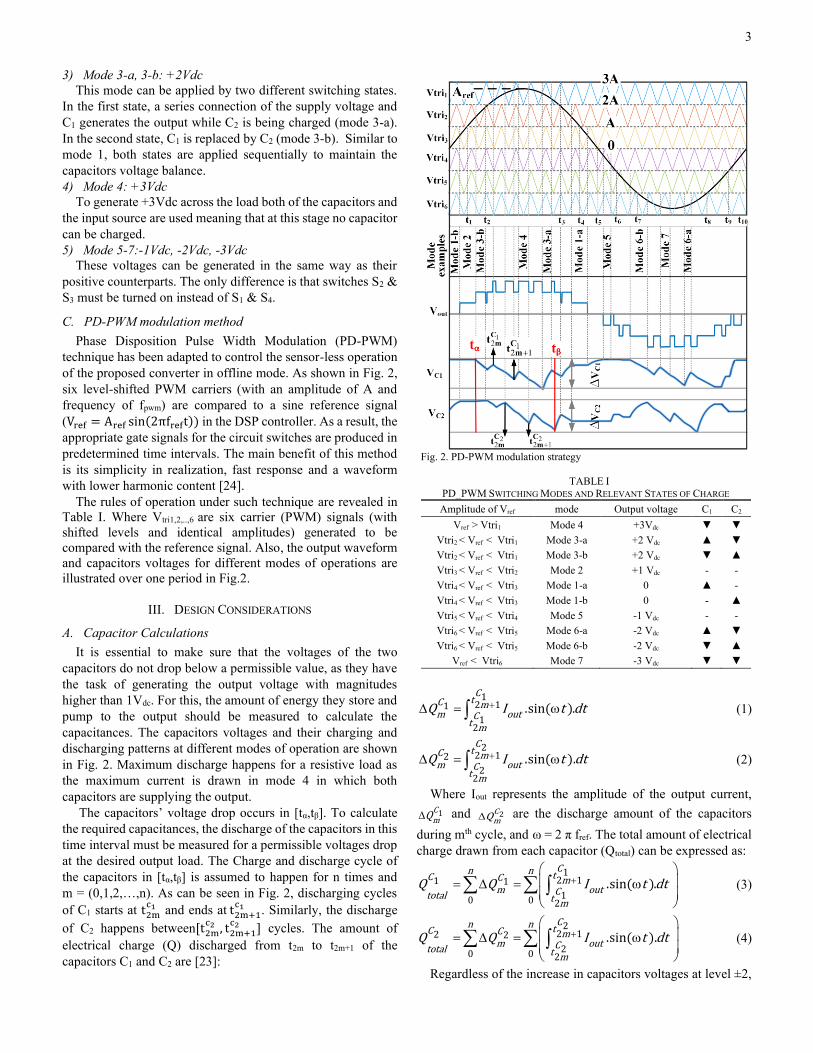
C. PD-PWM modulation method
Phase Disposition Pulse Width Modulation (PD-PWM)
technique has been adapted to control the sensor-less operation
of the proposed converter in offline mode. As shown in Fig. 2,
six level-shifted PWM carriers (with an amplitude of A and
frequency of fpwm) are compared to a sine reference signal
(Vref = Aref sin(2πfreft)) in the DSP controller. As a result, the
appropriate gate signals for the circuit switches are produced in
predetermined time intervals. The main benefit of this method
is its simplicity in realization, fast response and a waveform
with lower harmonic content [24].
The rules of operation under such technique are revealed in
Table I. Where Vtri1,2,..,6 are six carrier (PWM) signals (with
shifted levels and identical amplitudes) generated to be
compared with the reference signal. Also, the output waveform
and capacitors voltages for different modes of operations are
illustrated over one period in Fig.2.
III. DESIGN CONSIDERATIONS
A. Capacitor Calculations
It is essential to make sure that the voltages of the two
capacitors do not drop below a permissible value, as they have
the task of generating the output voltage with magnitudes
higher than 1Vdc. For this, the amount of energy they store and
pump to the output should be measured to calculate the
capacitances. The capacitors voltages and their charging and
discharging patterns at different modes of operation are shown
in Fig. 2. Maximum discharge happens for a resistive load as
the maximum current is drawn in mode 4 in which both
capacitors are supplying the output.
The capacitors’ voltage drop occurs in [tα,tβ]. To calculate
the required capacitances, the discharge of the capacitors in this
time interval must be measured for a permissible voltages drop
at the desired output load. The Charge and discharge cycle of
the capacitors in [tα,tβ] is assumed to happen for n times and
m = (0,1,2,…,n). As can be seen in Fig. 2, discharging cycles
of C1 starts at t2mc1 and ends at t2m+1
c1 . Similarly, the discharge
of C2 happens between[t2mc2 , t2m+1
c2 ] cycles. The amount of
electrical charge (Q) discharged from t2m to t2m+1 of the
capacitors C1 and C2 are [23]:
12 11
12
.sin( ).C
tC mm outC
t m
Q I t dt+ = (1)
22 12
22
.sin( ).C
tC mm outC
t m
Q I t dt+ = (2)
Where Iout represents the amplitude of the output current,
1CmQ and 2C
mQ are the discharge amount of the capacitors
during mth cycle, and ω = 2 π fref. The total amount of electrical
charge drawn from each capacitor (Qtotal) can be expressed as:
12 11 1
10 0 2
.sin( ).Cn n tC C m
m outCtotal t m
Q Q I t dt+ = =
(3)
22 12 2
20 0 2
.sin( ).Cn n tC C m
m outCtotal t m
Q Q I t dt+ = =
(4)
Regardless of the increase in capacitors voltages at level ±2,
Fig. 2. PD-PWM modulation strategy
TABLE I
PD_PWM SWITCHING MODES AND RELEVANT STATES OF CHARGE
Amplitude of Vref mode Output voltage C1 C2
Vref > Vtri1 Mode 4 +3Vdc
Vtri2 < Vref < Vtri1 Mode 3-a +2 Vdc
Vtri2 < Vref < Vtri1 Mode 3-b +2 Vdc
Vtri3 < Vref < Vtri2 Mode 2 +1 Vdc - -
Vtri4 < Vref < Vtri3 Mode 1-a 0 -
Vtri4 < Vref < Vtri3 Mode 1-b 0 -
Vtri5 < Vref < Vtri4 Mode 5 -1 Vdc - -
Vtri6 < Vref < Vtri5 Mode 6-a -2 Vdc
Vtri6 < Vref < Vtri5 Mode 6-b -2 Vdc
Vref < Vtri6 Mode 7 -3 Vdc
4
assuming the worst case in which no charge is absorbed by the
capacitors, the minimum allowable capacitance can be
formulated as:
1
1min 1
C
totalCripple
QC
V= ,
2
2min 2
C
totalCripple
QC
V= (5)
By assuming 𝑉𝑟𝑖𝑝𝑝𝑙𝑒𝐶 below 10%, recovery of the capacitors
voltage at levels 0 and ±2 will be assured. Also, it is noticeable
that no capacitors are charged or discharged at level ±1.
B. Power Loss Study
Power loss of the proposed converter can generally be
classified into three categories:
• Switching losses (Psw)
• Conduction losses (Pcond)
• Capacitor voltage ripple (charging) losses
In the following, a brief discussion of each category and its
impact on efficiency in different load conditions is presented.
1) Switching loss
Switching energy losses of IGBTs (Esw) in each switching
cycle consist of turn-on loss (Eon) and turn-off loss (Eoff).
Switching losses are inherent characteristics of IGBTs,
specified by the manufacturer under predefined conditions.
These losses vary under different circumstances, including:
junction temperature (Tj), collector current (Ic), blocking
voltage (Vb), gate-emitter voltage (VGE) and gate resistance
(RGE). Therefore, the Esw can be calculated as:
( ). . . .sw on off T I V GEj c bE E E adj adj adj adj= + (6)
In which Eon and Eoff are losses presented by the IGBT
module datasheet in nominal condition and adjTj, adjIc, adjVb and
adjGE are adjustment factors for the aforementioned variable
conditions. Therefore, the total switching power loss for the
nine switches (Psw) can be defined as:
9 9
1 1
. .sw sw sw ref kk kk k
P P E f N= =
= = (7)
Nk is the number of times each switch is turned on and off in
one cycle of reference waveform. Switches S1, S2, S3 and S4 turn
on and off once per each PWM cycle while |Aref sin(ωt)| ≤ A
and stay on or off for the rest of the reference cycle time. S5,
S6, S7 and S8 turn on and off once per each 2 PWM cycles.
While, S9 turn on and off once for every PWM cycles. Thus:
𝑁𝑘 =
2𝑓𝑃𝑊𝑀
𝑠𝑖𝑛−1 𝑠𝑖𝑛(𝐴
𝐴𝑟𝑒𝑓)
𝜋𝑓𝑟𝑒𝑓 𝑘 = 1,2,3,4
𝑓𝑃𝑊𝑀
2𝑓𝑟𝑒𝑓 𝑘 = 5,6,7,8
𝑓𝑃𝑊𝑀
𝑓𝑟𝑒𝑓 𝑘 = 9
(8)
2) Conduction loss
Conduction losses occur due to current passing through
circuit components. In the proposed structure, the conduction
losses are the result of capacitors’ internal resistance (RESR)
losses and IGBTs/diodes losses. IGBT losses can be calculated
by multiplying the IGBT collector-emitter voltage (VCE) and
collector current (Ic). Likewise, Diode losses are the result of
the forward voltage drop (VF) while it conducts current (IF). The
output characteristics of IGBT (VCE) and Diode (VF) change at
different current and operation conditions. VCE and VF can be
calculated as follows:
0.CE CE CE cV V R I= + (9)
0.F F D FV V R I= + (10)
VCE0 and RCE are the adjusted IGBT parameters represent the
nonlinear relation between VCE and IC at circuit operation
conditions. similarly, VF0 and RD are adjusted Diode internal
voltage drop and ressitance, respectively. Therefore, equivalent
circuits of the proposed topology and its conductive loss factors
for each output levels are brought in Table II. It is worth
mentioning that loss factors RL and VL represent the path
resistance and internal voltage drop of semiconductor devices
for each level of the output, respectively. TABLE II
CIRCUIT CONDUCTIVE LOSS FACTORS
Vout
Level Equivalent Circuit
Loss factors
VL RL
0 Vdc 1 IGBT & 1 Diode 0 0
+CE FV V +CE DR R
±1 Vdc 2 IGBTs & 2 Diodes 0 0
2( )+CE FV V ( )2 +CE DR R
±2 Vdc 3 IGBTs, 1 Diode
& 1 Capacitor 0 03 +CE FV V 3 + +CE D ESRR R R
±3 Vdc 4 IGBTs & 2 Capacitors 0
4 CEV 4 2+CE ESRR R
According to Fig. 2, while |Aref sin(ωt)| ≤ A, the output goes
back and forth between levels L=0 & 1. Similarly, the output
alternate between levels L=1 & 2 and L=2 & 3 while
A≤|Aref sin(ωt)|≤ 2A and 2A≤|Aref sin(ωt)|≤ 3A, respectively.
For L=0, 1 and 2, the energy loss occurring in the
aforementioned states can be defined as follows [21]:
12
1
& 1
sin( )
sin( )sin( )
1
.sin( )
sin( )sin( )
1
+
+
+
− +
−
− =
− +
+ −
−
ref
L
out
ref
L
ref
L
out
ref
L
j
i
L Lcond
t
t
A t L AR
AI t
A t L AR
Adt
A t L AV
AI t
A t L AV
A
E
(11)
Energy loss happens at the following time intervals:
0 1 4 5 5 6 9 10
1 2 3 4 6 7 8 9
2 3 7 8
i j
t t , t t , t t , t t L 0
t t : t t , t t , t t , t t L 1
t t , t t L 2
− − − − =
− − − − − =
− − =
(12)
In which t1 =1
Arcsin (
A
Aref) , t2 =
1
Arcsin (
2A
Aref), t5= π/ω,
t10= 2π/ω, t3= t5-t2, t4= t5-t1, t6= t5+t1, t7= t5+t2, t8= t10-t2 and t9=
t10 -t1. Ultimately, the total conduction loss is: 0&1 1&2 2&3(4 4 2 )= + +L L L
cond ref cond cond condP f E E E (13)
3) Capacitor voltage ripple losses
The power losses caused by the difference between the input
and capacitors voltages, while they are paralleled to the source
can be calculated as follows:
5
2
1
1. .
2 =
= u
C k ref
k
P C V f (14)
In which, u represents the number of both capacitors’
charging states and then, ΔVk is charging Voltage ripple of the
capacitors. Finally, based on [21, 23], total power loss (Ploss)
and efficiency (η) of the proposed converter can be calculated
as follows:
1 2= + + +loss sw cond C CP P P P P (15)
100= +
out
out loss
P
P P (16)
C. Comparison with other topologies
Table III reveals a detailed comparison over the proposed
structure and other existing ones, in terms of number of circuit
components (switches, driver circuits, capacitors, and diodes),
number of input sources, Peak Inverse Voltage (PIV), Total
Standing Voltage (TSV), regenerative load ability and the
boosting ratio. PIV implies the maximum voltage which the
switch has to bear in the off-state. In some applications, the
number of switches may be low but some of the switches have
to work with high voltages. Besides, TSV is the sum of
standing/operating voltage (or simply sum of the PIV) of all the
switches that should also be considered. Boost ratio is defined
as the proportion of the output amplitude to the input source or
the sum of input sources in case if there is more than one source
is used.
In the context of step-up SC-MLI, it is essential to design a
topology to use maximum possible standard rating of the
switches. Therefore, reducing the number of switches by
increasing the standing voltage in standard range is an
important aspect which should be considered in comparison. In
fact, the input voltage could be raised until the PIV is less than
a certain acceptable percentage (x%) of the switches rated
voltage (𝑉𝑟𝑎𝑡𝑒𝑑𝑆𝑊 ) as follows:
%. SW
ratedPIV x V (17)
As can be seen in the Table III, unlike the proposed circuit,
authors in [3], [31] and [32] introduced structures that require
several isolated DC sources and the amplitude of the output
does not exceed the sum of input voltages. In case of [3] and
[32], it should be noted that using symmetric sources leads to a
5-level output waveform.
Although [20], [28] and [38-41] are single-source topologies
with voltage boosting ability and have relatively less
semiconductor devices (except for [28]), they cannot supply
regenerative loads. [26] and [34-37] present single source
structures with a considerably low TSV. However, they either
cannot boost the input voltage, or they have a low boosting
ratio. Also, they require more capacitors.
It is noticeable that topologies presented in [23], [24], and
[33] can meet both the boost ratio and regenerative capability
requirements, whereas the introduced SCMLI requires less
active switches and, therefore, less gate driver circuits for the
same output levels. Considering semiconductor count, boost
factor, and regenerative load ability, the proposed topology
should compete with [23], [24], and [33].
Selecting each switching device in an inverter is related to
the maximum voltage impressed and the peak and average
current going through it. Therefore, the product of voltage stress
TABLE III COMPARISON OF THE SUGGESTED SEVEN-LEVEL INVERTER WITH RECENT TOPOLOGIES
NO. Topology N
levels
N sw
itch
es
N d
iod
es
N d
riv
ers
N c
ap
acito
rs
N so
urc
es
PIV
(*V
in)
TS
V (*
Vin
)
Boo
st ratio
Reg
en
era
tive
Po
ut (W
)
Efficiency (%)
Theoretical Experimental
1 [31] 2018 7 10 10 7 0 3 3 19 1x Yes 50 N.A. 97.6
2 [32] 2017 7 8 8 8 0 2 2 12 1x Yes 250
N.A. 97
1000 98
3 [3] 2017 7 8 8 8 0 2 3 18 1x Yes 100 N.A. 94.3
4 [26] 2015 7 7 9 7 3 1 1 5 1x Yes 500 N.A. 91
5 [34] 2017 7 12 12 12 4 1 1 3.33 1x yes 500 N.A. N.A.
6 [35] 2012 7 14 14 12 5 1 1 3.33 1x yes 5000 N.A. N.A.
7 [36] 2018 7 10 10 8 3 1 1 8 1.5x yes 225 N.A. N.A.
8 [37] 2019 7 10 10 8 4 1 1 7.5 1.5x yes 266.2 96.5 96.5
9 [33] 2018 7 16 16 14 2 1 1 16 3x Yes 40 N.A. 94
10 [23] 2014 7 10 10 10 2 1 3 18 3x Yes 3.5 94.6 95.4
11 [24] 2016 7 16 16 14 2 1 1 16 3x Yes 200 93.8
N.A. 1000 90.2
12 Proposed 7 9 12 9 2 1 3 17 3x Yes
50 96.07 92
250 95.3 94.3
500 94.5 92.2
13 [38] 2018 7 9 10 8 3 1 1 7.5 1.5x No 218 N.A. 97.29
14 [20] 2014 7 7 11 7 2 1 3 21 3x No 247.5 N.A. 89.2
15 [28] 2018 7 14 14 14 2 1 1 14 3x No 182.4 91.7 88.93
16 [39] 2019 7 8 6 8 2 1 3 18 3x No N.A. N.A. N.A.
17 [40] 2019 7 8 10 8 2 1 3 16 3x No 189 N.A. 97.1
18 [41] 2014 7 8 10 8 2 1 3 18 3x No N.A. N.A. N.A.
6
and current stress is introduced as Switching Device Power
(SDP) index [42]. The sum of SDP of all the switching devices
used in the circuit is an important factor of an inverter.
Considering the number of switching devices used (N), the peak
voltage impressed on the devices (Vk), Ik,average and Ik,peak as the
average and peak current through the device, respectively, then:
,1
SDP= .Iavg
N
k k averagek
Total Average SDP V=
= (18)
,1
SDP= .Ipeak
N
k k peakk
Total Peak SDP V=
= (19)
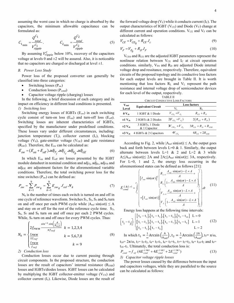
The SDP of all topologies with boosting ability for the same
conditions including semiconductor device properties, output
power (Pout=750W, Vout_max=375V), load power factor (PF=1)
and input voltage (Vin= 125V) are summarized as depicted in
Fig. 3. As the number of semiconductors decreases, the amount
of SDPave increases. Thus, non-regenerative structures with less
semiconductors have a higher SDPave. Furthermore, for the
Switched-Capacitor Structures the amount of SDPpeak directly
depends on the resistance of capacitors charging paths. Changes
in the charging paths resistance changes the peak current of the
semiconductors. However, as (14) shows, it does not affect the
capacitors charging loss. Consequently, the corresponding
SDPpeak of the proposed SCMLI is better than the other
topologies whereas its SDPave is within the range of them.
IV. EXPERIMENTAL RESULTS
In this section, the design characteristics and experimental
results of the proposed 7-level inverter under various
conventional (static and transient) and regenerative load
conditions are discussed. In order to verify the feasibility of the
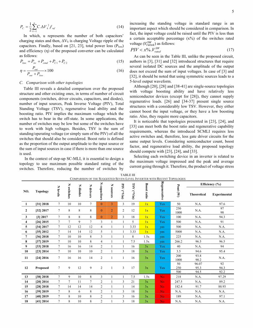
proposed topology and assess its performance, a laboratory
prototype is implemented (see Fig 4). Furthermore, the
specifications of this setup are brought in Table IV. A
TMS320F28335 DSP processor was used to create gate pulses
based on the phase disposition technique. Then, these pulses
were isolated and amplified by a circuit consisting of
HCPL3120 isolator IC.
When the phase difference between load voltage and current
is below 90º (0≤φ<90), their polarity are the same for most of
the cycle. Thus, the average power is supplied to the load and
the overall performance of the inverter is considered to be
inverting. Whenever the phase difference between load voltage
and current is above 90º (90<φ<180), their polarity differs for
most of the cycle. Hence, the inverter pumps average power
from the AC to the DC side and the overall performance of the
inverter is considered to be rectification (or regeneration) [22].
This feature is crucial in switched-capacitor structures to
prevent the capacitors from over-charge, feeding the excess
charge to the input source, instead.
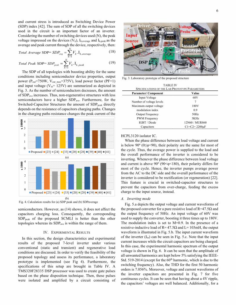
A. Inverting mode
Fig. 5.a depicts the output voltage and current waveforms of
the proposed converter for a pure resistive load of R=47.5Ω and
the output frequency of 50Hz. An input voltage of 60V was
used to supply the converter, boosting it three times up to 180V.
The modulation index is set to M=0.9. In the presence of a
resistive-inductive load of R= 47.5Ω and L= 103mH, the output
waveform is illustrated in Fig. 5.b. The input current waveform
of the inverter (Iin) can be seen in Fig. 5.c. Note that the input
current increases while the circuit capacitors are being charged.
In this case, the experimental harmonic spectrum of the output
voltage is shown in Fig. 6. It can be seen that the amplitude of
all unwanted harmonics are kept below 5% satisfying the IEEE-
Std. 519-2014 (except for the 60th harmonic, which is due to the
switching frequency). Also, the THD for the first 50 harmonic
orders is 7.056%. Moreover, voltage and current waveforms of
the inverter capacitors are presented in Fig. 7 for five
continuous cycles. It can be seen that having about a 4V ripple,
the capacitors’ voltages are well balanced. Additionally, for a
(a)
(b)
Fig. 4. Calculation results for (a) SDP peak and (b) SDPaverage
0
1
2
3
4
x 1
00
00
Proposed [23] [24] [33] [20] [28] [39] [40] [41]
0
1
2
3
4
x 1
00
0
Proposed [23] [24] [33] [20] [28] [39] [40] [41]
Fig. 3. Laboratory prototype of the proposed structure
TABLE IV
SPECIFICATIONS OF THE LAB PROTOTYPE PARAMETERS
Parameter/ Component Value
Input Voltage 60V
Number of voltage levels 7
Maximum output voltage 180V
modulation index 0.9
Output Frequency 50Hz
PWM Frequency 3KHz
IGBT / Diode 12N60 / MUR860
Capacitors C1=C2= 2200μF
7
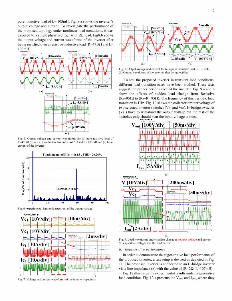
pure inductive load of L= 103mH, Fig. 8.a shows the inverter’s
output voltage and current. To investigate the performance of
the proposed topology under nonlinear load conditions, it was
exposed to a single phase rectifier with RL load. Fig8.b shows
the output voltage and current waveforms of the inverter after
being rectified over a resistive-inductive load (R=47.5Ω and L=
103mH).
Fig. 5. Output voltage and current waveforms for (a) pure resistive load of
R=47.5Ω (b) resistive-inductive load of R=47.5Ω and L= 103mH and (c) Input current of the inverter
Fig. 6. experimental harmonic spectrum of the output voltage
Fig. 7. Voltage and current waveforms of the inverter capacitors
Fig. 8. Output voltage and current for (a) a pure inductive load (L=103mH) (b) Output waveforms of the inverter after being rectified
To test the proposed inverter in transient load conditions,
different load transition cases have been studied. These tests
suggest the proper performance of the inverter. Fig. 9.a and b
show the effects of sudden load change from Resistive
(R1=95Ω) to (R2=R1||95Ω). The frequency of this periodic load
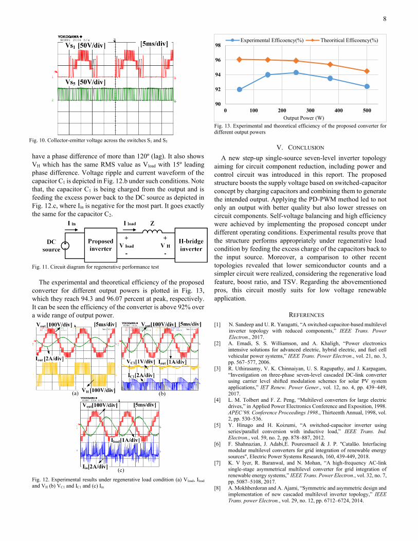
transition is 1Hz. Fig. 10 shows the collector-emitter voltage of
two selected inverter switches (Vs1 and Vs5). H-bridge switches
(Vs1) have to withstand the output voltage but the rest of the
switches only should bear the input voltage at most.
(a)
(b)
Fig. 9. Load waveforms under sudden change (a) output voltage and current (b) capacitors voltages and the load current
B. Regenerative performance
In order to demonstrate the regenerative load performance of
the proposed inverter, a test setup is devised as depicted in Fig.
11. The proposed inverter is connected to an H-bridge inverter
via a line impedance (z) with the value of (R=2Ω, L=107mH).
Fig. 12 illustrates the experimental results under regenerative
load condition. Fig. 12.a presents the Vload and Iload, where they
8
have a phase difference of more than 120º (lag). It also shows
VH which has the same RMS value as Vload with 15º leading
phase difference. Voltage ripple and current waveform of the
capacitor C1 is depicted in Fig. 12.b under such conditions. Note
that, the capacitor C1 is being charged from the output and is
feeding the excess power back to the DC source as depicted in
Fig. 12.c, where Iin is negative for the most part. It goes exactly
the same for the capacitor C2.
Fig. 11. Circuit diagram for regenerative performance test
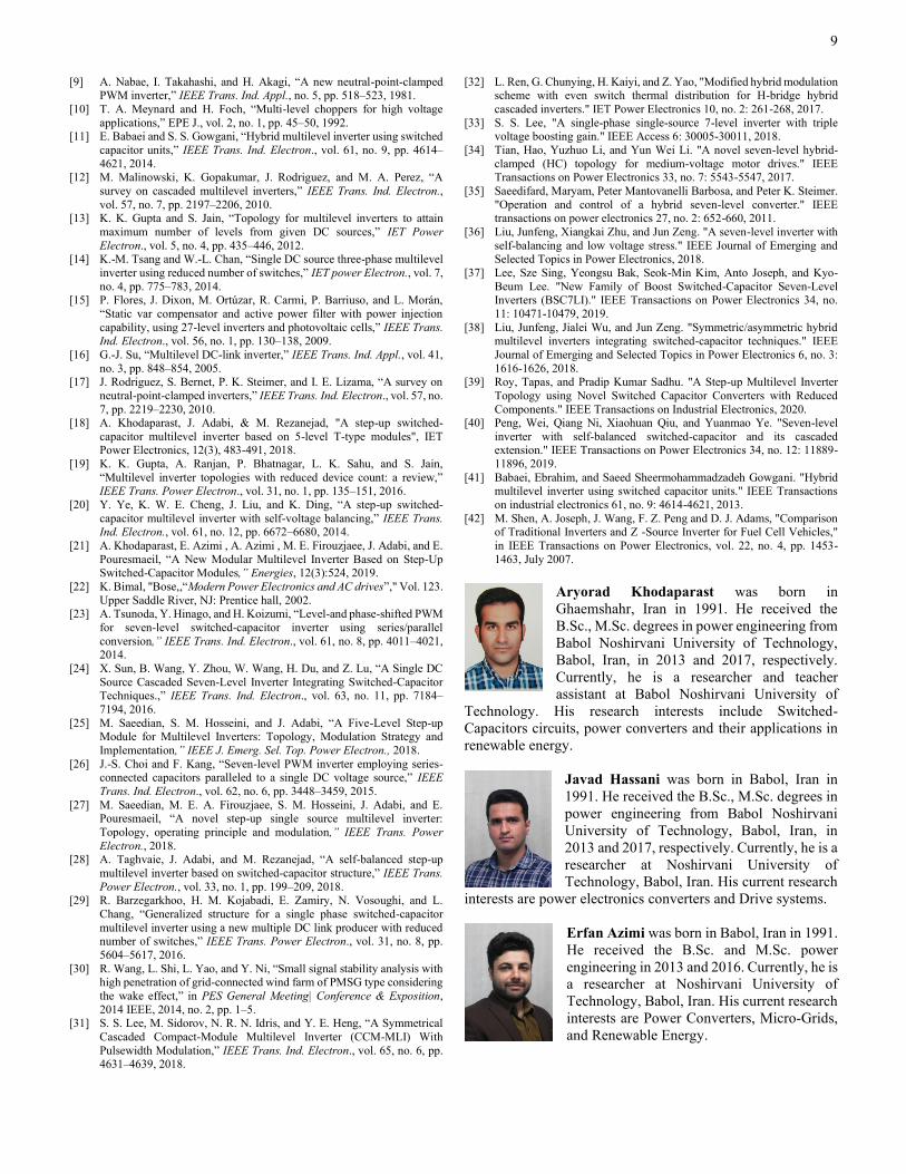
The experimental and theoretical efficiency of the proposed
converter for different output powers is plotted in Fig. 13,
which they reach 94.3 and 96.07 percent at peak, respectively.
It can be seen the efficiency of the converter is above 92% over
a wide range of output power.
Fig. 12. Experimental results under regenerative load condition (a) Vload, Iload and VH (b) VC1 and IC1 and (c) Iin
Fig. 13. Experimental and theoretical efficiency of the proposed converter for different output powers
V. CONCLUSION
A new step-up single-source seven-level inverter topology
aiming for circuit component reduction, including power and
control circuit was introduced in this report. The proposed
structure boosts the supply voltage based on switched-capacitor
concept by charging capacitors and combining them to generate
the intended output. Applying the PD-PWM method led to not
only an output with better quality but also lower stresses on
circuit components. Self-voltage balancing and high efficiency
were achieved by implementing the proposed concept under
different operating conditions. Experimental results prove that
the structure performs appropriately under regenerative load
condition by feeding the excess charge of the capacitors back to
the input source. Moreover, a comparison to other recent
topologies revealed that lower semiconductor counts and a
simpler circuit were realized, considering the regenerative load
feature, boost ratio, and TSV. Regarding the abovementioned
pros, this circuit mostly suits for low voltage renewable
application.
REFERENCES
[1] N. Sandeep and U. R. Yaragatti, “A switched-capacitor-based multilevel
inverter topology with reduced components,” IEEE Trans. Power
Electron., 2017. [2] A. Emadi, S. S. Williamson, and A. Khaligh, “Power electronics
intensive solutions for advanced electric, hybrid electric, and fuel cell
vehicular power systems,” IEEE Trans. Power Electron., vol. 21, no. 3, pp. 567–577, 2006.
[3] R. Uthirasamy, V. K. Chinnaiyan, U. S. Ragupathy, and J. Karpagam,
“Investigation on three-phase seven-level cascaded DC-link converter using carrier level shifted modulation schemes for solar PV system
applications,” IET Renew. Power Gener., vol. 12, no. 4, pp. 439–449,
2017. [4] L. M. Tolbert and F. Z. Peng, “Multilevel converters for large electric
drives,” in Applied Power Electronics Conference and Exposition, 1998.
APEC’98. Conference Proceedings 1998., Thirteenth Annual, 1998, vol. 2, pp. 530–536.
[5] Y. Hinago and H. Koizumi, “A switched-capacitor inverter using
series/parallel conversion with inductive load,” IEEE Trans. Ind. Electron., vol. 59, no. 2, pp. 878–887, 2012.
[6] F. Shahnazian, J. Adabi,E. Pouresmaeil & J. P. "Catalão. Interfacing
modular multilevel converters for grid integration of renewable energy sources", Electric Power Systems Research, 160, 439-449, 2018.
[7] K. V Iyer, R. Baranwal, and N. Mohan, “A high-frequency AC-link
single-stage asymmetrical multilevel converter for grid integration of renewable energy systems,” IEEE Trans. Power Electron., vol. 32, no. 7,
pp. 5087–5108, 2017.
[8] A. Mokhberdoran and A. Ajami, “Symmetric and asymmetric design and implementation of new cascaded multilevel inverter topology,” IEEE
Trans. power Electron., vol. 29, no. 12, pp. 6712–6724, 2014.
90
92
94
96
98
0 100 200 300 400 500
Output Power (W)
Experimental Efficoency(%) Theoritical Efficoency(%)
Fig. 10. Collector-emitter voltage across the switches S1 and S5
9
[9] A. Nabae, I. Takahashi, and H. Akagi, “A new neutral-point-clamped PWM inverter,” IEEE Trans. Ind. Appl., no. 5, pp. 518–523, 1981.
[10] T. A. Meynard and H. Foch, “Multi-level choppers for high voltage
applications,” EPE J., vol. 2, no. 1, pp. 45–50, 1992. [11] E. Babaei and S. S. Gowgani, “Hybrid multilevel inverter using switched
capacitor units,” IEEE Trans. Ind. Electron., vol. 61, no. 9, pp. 4614–
4621, 2014. [12] M. Malinowski, K. Gopakumar, J. Rodriguez, and M. A. Perez, “A
survey on cascaded multilevel inverters,” IEEE Trans. Ind. Electron.,
vol. 57, no. 7, pp. 2197–2206, 2010. [13] K. K. Gupta and S. Jain, “Topology for multilevel inverters to attain
maximum number of levels from given DC sources,” IET Power
Electron., vol. 5, no. 4, pp. 435–446, 2012. [14] K.-M. Tsang and W.-L. Chan, “Single DC source three-phase multilevel
inverter using reduced number of switches,” IET power Electron., vol. 7,
no. 4, pp. 775–783, 2014. [15] P. Flores, J. Dixon, M. Ortúzar, R. Carmi, P. Barriuso, and L. Morán,
“Static var compensator and active power filter with power injection
capability, using 27-level inverters and photovoltaic cells,” IEEE Trans.
Ind. Electron., vol. 56, no. 1, pp. 130–138, 2009.
[16] G.-J. Su, “Multilevel DC-link inverter,” IEEE Trans. Ind. Appl., vol. 41,
no. 3, pp. 848–854, 2005. [17] J. Rodriguez, S. Bernet, P. K. Steimer, and I. E. Lizama, “A survey on
neutral-point-clamped inverters,” IEEE Trans. Ind. Electron., vol. 57, no.
7, pp. 2219–2230, 2010. [18] A. Khodaparast, J. Adabi, & M. Rezanejad, "A step-up switched-
capacitor multilevel inverter based on 5-level T-type modules", IET Power Electronics, 12(3), 483-491, 2018.
[19] K. K. Gupta, A. Ranjan, P. Bhatnagar, L. K. Sahu, and S. Jain,
“Multilevel inverter topologies with reduced device count: a review,” IEEE Trans. Power Electron., vol. 31, no. 1, pp. 135–151, 2016.
[20] Y. Ye, K. W. E. Cheng, J. Liu, and K. Ding, “A step-up switched-
capacitor multilevel inverter with self-voltage balancing,” IEEE Trans. Ind. Electron., vol. 61, no. 12, pp. 6672–6680, 2014.
[21] A. Khodaparast, E. Azimi , A. Azimi , M. E. Firouzjaee, J. Adabi, and E.
Pouresmaeil, “A New Modular Multilevel Inverter Based on Step-Up
Switched-Capacitor Modules,” Energies, 12(3):524, 2019.
[22] K. Bimal, "Bose,,“Modern Power Electronics and AC drives”," Vol. 123.
Upper Saddle River, NJ: Prentice hall, 2002. [23] A. Tsunoda, Y. Hinago, and H. Koizumi, “Level-and phase-shifted PWM
for seven-level switched-capacitor inverter using series/parallel
conversion,” IEEE Trans. Ind. Electron., vol. 61, no. 8, pp. 4011–4021, 2014.
[24] X. Sun, B. Wang, Y. Zhou, W. Wang, H. Du, and Z. Lu, “A Single DC
Source Cascaded Seven-Level Inverter Integrating Switched-Capacitor Techniques.,” IEEE Trans. Ind. Electron., vol. 63, no. 11, pp. 7184–
7194, 2016.
[25] M. Saeedian, S. M. Hosseini, and J. Adabi, “A Five-Level Step-up Module for Multilevel Inverters: Topology, Modulation Strategy and
Implementation,” IEEE J. Emerg. Sel. Top. Power Electron., 2018.
[26] J.-S. Choi and F. Kang, “Seven-level PWM inverter employing series-connected capacitors paralleled to a single DC voltage source,” IEEE
Trans. Ind. Electron., vol. 62, no. 6, pp. 3448–3459, 2015.
[27] M. Saeedian, M. E. A. Firouzjaee, S. M. Hosseini, J. Adabi, and E. Pouresmaeil, “A novel step-up single source multilevel inverter:
Topology, operating principle and modulation,” IEEE Trans. Power
Electron., 2018. [28] A. Taghvaie, J. Adabi, and M. Rezanejad, “A self-balanced step-up
multilevel inverter based on switched-capacitor structure,” IEEE Trans.
Power Electron., vol. 33, no. 1, pp. 199–209, 2018. [29] R. Barzegarkhoo, H. M. Kojabadi, E. Zamiry, N. Vosoughi, and L.
Chang, “Generalized structure for a single phase switched-capacitor
multilevel inverter using a new multiple DC link producer with reduced number of switches,” IEEE Trans. Power Electron., vol. 31, no. 8, pp.
5604–5617, 2016.
[30] R. Wang, L. Shi, L. Yao, and Y. Ni, “Small signal stability analysis with high penetration of grid-connected wind farm of PMSG type considering
the wake effect,” in PES General Meeting| Conference & Exposition,
2014 IEEE, 2014, no. 2, pp. 1–5. [31] S. S. Lee, M. Sidorov, N. R. N. Idris, and Y. E. Heng, “A Symmetrical
Cascaded Compact-Module Multilevel Inverter (CCM-MLI) With
Pulsewidth Modulation,” IEEE Trans. Ind. Electron., vol. 65, no. 6, pp. 4631–4639, 2018.
[32] L. Ren, G. Chunying, H. Kaiyi, and Z. Yao, "Modified hybrid modulation scheme with even switch thermal distribution for H-bridge hybrid
cascaded inverters." IET Power Electronics 10, no. 2: 261-268, 2017.
[33] S. S. Lee, "A single-phase single-source 7-level inverter with triple voltage boosting gain." IEEE Access 6: 30005-30011, 2018.
[34] Tian, Hao, Yuzhuo Li, and Yun Wei Li. "A novel seven-level hybrid-
clamped (HC) topology for medium-voltage motor drives." IEEE Transactions on Power Electronics 33, no. 7: 5543-5547, 2017.
[35] Saeedifard, Maryam, Peter Mantovanelli Barbosa, and Peter K. Steimer.
"Operation and control of a hybrid seven-level converter." IEEE transactions on power electronics 27, no. 2: 652-660, 2011.
[36] Liu, Junfeng, Xiangkai Zhu, and Jun Zeng. "A seven-level inverter with
self-balancing and low voltage stress." IEEE Journal of Emerging and Selected Topics in Power Electronics, 2018.
[37] Lee, Sze Sing, Yeongsu Bak, Seok-Min Kim, Anto Joseph, and Kyo-
Beum Lee. "New Family of Boost Switched-Capacitor Seven-Level Inverters (BSC7LI)." IEEE Transactions on Power Electronics 34, no.
11: 10471-10479, 2019.
[38] Liu, Junfeng, Jialei Wu, and Jun Zeng. "Symmetric/asymmetric hybrid
multilevel inverters integrating switched-capacitor techniques." IEEE
Journal of Emerging and Selected Topics in Power Electronics 6, no. 3:
1616-1626, 2018. [39] Roy, Tapas, and Pradip Kumar Sadhu. "A Step-up Multilevel Inverter
Topology using Novel Switched Capacitor Converters with Reduced
Components." IEEE Transactions on Industrial Electronics, 2020. [40] Peng, Wei, Qiang Ni, Xiaohuan Qiu, and Yuanmao Ye. "Seven-level
inverter with self-balanced switched-capacitor and its cascaded extension." IEEE Transactions on Power Electronics 34, no. 12: 11889-
11896, 2019.
[41] Babaei, Ebrahim, and Saeed Sheermohammadzadeh Gowgani. "Hybrid multilevel inverter using switched capacitor units." IEEE Transactions
on industrial electronics 61, no. 9: 4614-4621, 2013. [42] M. Shen, A. Joseph, J. Wang, F. Z. Peng and D. J. Adams, "Comparison
of Traditional Inverters and Z -Source Inverter for Fuel Cell Vehicles,"
in IEEE Transactions on Power Electronics, vol. 22, no. 4, pp. 1453-
1463, July 2007.
Aryorad Khodaparast was born in
Ghaemshahr, Iran in 1991. He received the
B.Sc., M.Sc. degrees in power engineering from
Babol Noshirvani University of Technology,
Babol, Iran, in 2013 and 2017, respectively.
Currently, he is a researcher and teacher
assistant at Babol Noshirvani University of
Technology. His research interests include Switched-
Capacitors circuits, power converters and their applications in
renewable energy.
Javad Hassani was born in Babol, Iran in
1991. He received the B.Sc., M.Sc. degrees in
power engineering from Babol Noshirvani
University of Technology, Babol, Iran, in
2013 and 2017, respectively. Currently, he is a
researcher at Noshirvani University of
Technology, Babol, Iran. His current research
interests are power electronics converters and Drive systems.
Erfan Azimi was born in Babol, Iran in 1991.
He received the B.Sc. and M.Sc. power
engineering in 2013 and 2016. Currently, he is
a researcher at Noshirvani University of
Technology, Babol, Iran. His current research
interests are Power Converters, Micro-Grids,
and Renewable Energy.
10
M. Ebrahim Adabi was born in 1985. He
received the B.Sc. and M.Sc. degrees in
Electrical Engineering in 2008 and 2011, and
the Ph.D. degree in Electrical Engineering
from Universitat Politecnica de Catalunya
(UPC), Barcelona, Spain in 2018. He is
currently a Postdoctoral Researcher with
Ecole Centrale de Nantes in Laboratoire des
Sciences du Numériques de Nantes, Nantes, France. His
research interests include design and modeling of power
electronic converters for renewable energy applications, and
modular multilevel converters.
Jafar Adabi was born in 1981. He received
his BEng and MEng degrees from
Mazandaran University, Babol, Iran, in 2004
and 2006, respectively. He finished his PhD
degree in the School of Engineering Systems
at the Queensland University of Technology,
Brisbane, Queensland, Australia at 2010.
Currently, he is an associate professor at Babol Noshirvani
University of Technology, Babol, Iran. His research interests
are the optimal design and high frequency modelling of power
electronics and motor drive systems for EMI analysis.
Edris Pouresmaeil (M'14-SM'17)
received the Ph.D. degree in Electrical
Engineering from Technical University of
Catalonia (UPC-Barcelona Tech), Barcelona,
Spain, in 2012. After his Ph.D., he joined the
University of Waterloo, Waterloo, Canada as
a Post-Doctoral Research Fellow and then
joined the University of Southern Denmark (SDU), Odense,
Denmark, as an Associate Professor. He is currently an
Associate Professor with the Department of Electrical
Engineering and Automation (EEA) at Aalto University, Espoo,
Finland. His main research activities focus on the application of
power electronics in power and energy sectors.


![AZIMI, K et al [2010] ASPARAGUS IN PERU Microeconomics of Competitiveness.pdf](https://img.pdfslide.us/doc/110x75/577cc5ee1a28aba7119d5d4c/azimi-k-et-al-2010-asparagus-in-peru-microeconomics-of-competitivenesspdf.jpg)