Embed Size (px)
Citation preview
Keysight EEsof EDAMicrowave Discrete and Microstrip Filter Design
Demo Guide

02 | Keysight | Microwave Discrete and Microstrip Filter Design - Demo Guide
Theory
Microwave filters play an important role in any RF front end for the suppression of out of band signals. In the lumped and distributed form, they are extensively used for both commercial and military applications. A filter is a reactive network that passes a desired band of frequencies while almost stopping all other bands of frequencies. The frequency that separates the transmission band from the attenuation band is called the cutoff frequency and denoted as fc. The attenuation of the filter is denoted in decibels or nepers. A filter in general can have any number of pass bands separated by stop bands. They are mainly classified into four common types, namely lowpass, highpass, bandpass and band stop filters.
An ideal filter should have zero insertion loss in the pass band, infinite attenuation in the stop band and a linear phase response in the pass band. An ideal filter cannot be realizable as the response of an ideal low pass or band pass filter is a rectangular pulse in the frequency domain. The art of filter design necessitates compromises with respect to cutoff and roll off. There are basically three methods for filter synthesis. They are the image parameter method, Insertion loss method and numerical synthesis. The image parameter method is an old and crude method whereas the numerical method of synthesis is newer but cumbersome. The insertion loss method of filter design on the other hand is the optimum and more popular method for higher frequency applications. The filter design flow for insertion loss method is shown below.
Select prototype for desired responsecharacteristics (always yields normalized
values and low-pass network)
OR BPFLPF
OTHER STRUCTURES FOR HPF, BPF
INS
ERTI
ON
-LO
SS
Transform for desired frequency bandand characteristic impedance
(yields lumped network)
Realize result of step 2 in suitablemicrowave form (e.g. Microstrip)
Cascaded microstrip lines,each section < λg/4
Convert to single type resonators thenuse parallel-coupled half wave resonator
cascade realization
Figure 131.
03 | Keysight | Microwave Discrete and Microstrip Filter Design - Demo Guide
Since the characteristics of an ideal filter cannot be obtained, the goal of filter design is to approximate the ideal requirements within an acceptable tolerance. There are four types of approximations namely Butterworth or maximally flat, Chebyshev, Bessel and Elliptic approximations. For the proto type filters, maximally flat or Butterworth provides the flattest pass band response for a given filter order. In the Chebyshev method, sharper cutoff is achieved and the pass band response will have ripples of amplitude 1+k2. Bessel approximations are based on the Bessel function, which provides sharper cutoff and Elliptic approximations results in pass band and stop band ripples. Depending on the application and the cost, the approximations can be chosen. The optimum filter is the Chebyshev filter with respect to response and the bill of materials. Filter can be designed both in the lumped and distributed form using the above approximations.
Design of Microwave FiltersThe first step in the design of Microwave filters is to select a suitable approximation of the prototype model based on the specifications.
Calculate the order of the filter from the necessary roll off as per the given specifications. The order can be calculated as follows:
Butterworth Approximation:
LA (ω ′) = 10log 10 1+ ε (ω ’/ ωc) 2N
Where ε = Antilog10 LA/10 -1 and LA= 3 dB for Butterworth
Chebyshev Approximation:
Where, ωc is the angular cutoff frequency
ω’ is the angular attenuation frequency
LA(ω’) is the attenuation at ω’
N is the order of the filter
ε = Antilog10 LAr /10 -1 and LAr = Ripple in passband
The next step in the filter design is to calculate the prototype values of the filter depending on the type of approximation. The prototype values for the Chebyshev and Butterworth approximations can be calculated using the given equations.
04 | Keysight | Microwave Discrete and Microstrip Filter Design - Demo Guide
Butterworth Approximation:
g0 =1,
gk = 2sin (2k-1)π/2n where k = 1,2,….n and
gN+1 =1
Where, n is the order of the filter
Chebyshev Approximation:The element values may be computed as follows
After computing the prototype values the prototype filter has to be transformed with respect to frequency and impedance to meet the specifications. The transformations can be done using the following equations.
For Lowpass filter:
After Impedance and frequency scaling:
C’k=Ck/R0 ω c
L’k=R0Lk/ω c Where R0 = 50 Ω

05 | Keysight | Microwave Discrete and Microstrip Filter Design - Demo Guide
For the distributed design, the electrical length is given by:
Length of capacitance section: ZI/R0 Ck,Length of inductance section: Lk R0/Zh
Where, Zl is the low impedance value and Zh is the high impedance value
For bandpass filter:
Impedance and frequency scaling:
L’1 =L1Z0/ω0∆ C’1= ∆/L1Z0 ω 0
L’2 = ∆ Z0/ω 0C2
C’2=C2/Z0 ∆ ω 0
L’3 =L3Z0/ω 0 ∆
C’3= ∆/L3Z0 ω 0
Where, ∆ is the fractional bandwidth ∆ = ( ω 2- ω 1)/ ω 0
Typical DesignCutoff Frequency (fc) : 2 GHz
Attenuation at (f = 4 GHz) : 30 dB (LA(ω))
Type of approximation : Butterworth
Order of the filter : LA (ω) = 10log10 1+ε (ω/ ωc) 2N
Where, ε = Antilog10 LA/10 -1
Substituting the values of LA (ω), ω and ωc, the value of N is calculated to be 4.
Prototype Values of the Lowpass FilterThe prototype values of the filter is calculated using the formula given by
g0 =1,
gk = 2sin (2k-1)π/2N where k = 1,2,….N
and gN+1 =1
Simulation of a Lumped and Distributed Lowpass Filter Using ADS

06 | Keysight | Microwave Discrete and Microstrip Filter Design - Demo Guide
The prototype values for the given specifications of the filter are
g1 = 0.7654 = C1, g2 = 1.8478 = L2, g3 = 1.8478 = C3
& g4 = 0.7654 = L4
Lumped Model of the FilterThe Lumped values of the Lowpass filter after frequency and impedance scaling are given by:
Ck’= Ck /R0ωc
Lk’=R0 Lk /ωc where R0 is 50 Ω
The resulting lumped values are given by C1 = 1.218 pF, L2 = 7.35 nH, C3 = 2.94 pF and L4 = 3.046 nH
Distributed Model of the FilterFor distributed design, the electrical length is given by
Length of capacitance section (βLc) : Ck Zl/R0
Length of inductance section (βLi) : Lk R0/Zh
Where,
Zl is the low impedance value
Zh is the high impedance value
R0 is the Source and load impedance
ωc is the desired cutoff frequency
If we consider Zl = 10 Ω and Zh = 100 Ω then βLc1 = 0.153, βLi2 = 0.9239,
βLc3 = 0.3695 and βLi4 = 0.3827
Since β = 2π/λ, the physical lengths are given by
Lc1 = 1.68 mm
Li2 = 10.145 mm
Lc3 = 4.057 mm and
Li4 = 4.202 mm
07 | Keysight | Microwave Discrete and Microstrip Filter Design - Demo Guide
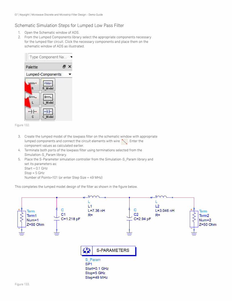
Schematic Simulation Steps for Lumped Low Pass Filter1. Open the Schematic window of ADS.2. From the Lumped Components library select the appropriate components necessary
for the lumped filer circuit. Click the necessary components and place them on the schematic window of ADS as illustrated.
3. Create the lumped model of the lowpass filter on the schematic window with appropriate lumped components and connect the circuit elements with wire . Enter the component values as calculated earlier.
4. Terminate both ports of the lowpass filter using terminations selected from the Simulation-S_Param library.
5. Place the S-Parameter simulation controller from the Simulation-S_Param library and set its parameters as:
Start = 0.1 GHz Stop = 5 GHz Number of Points=101 (or enter Step Size = 49 MHz)
This completes the lumped model design of the filter as shown in the figure below.
Figure 132.
Figure 133.

08 | Keysight | Microwave Discrete and Microstrip Filter Design - Demo Guide
6. Simulate the circuit by clicking F7 or the simulation gear icon.7. After the simulation is complete, ADS automatically opens the Data Display window
displaying the results. If the Data Display window does not open, click Window > New Data Display. In the data display window, select a rectangular plot and this automatically opens the place attributes dialog box. Select the traces to be plotted (in our case S(1,1) & S(2,1) are plotted in dB) and click Add>>.
8. Click and insert a marker on S(2,1) trace around 2GHz to see the data display graph as shown below.
Figure 134.
Results and ObservationsIt is observed from the schematic simulation that the lumped model of the lowpass filter has a cutoff of 2 GHz and a roll off as per the specifications.
Layout Simulation Steps for Distributed Low Pass FilterCalculate the physical parameters of the distributed lowpass filter using the design procedure given above. Calculate the width of the Zl and Zh transmission lines for the design of the stepped impedance lowpass filter. In this case Zl = 10 Ω and Zh = 100 Ω and the corresponding line widths are 24.7 mm and 0.66 mm respectively for a dielectric constant of 4.6 and a thickness of 1.6 mm.
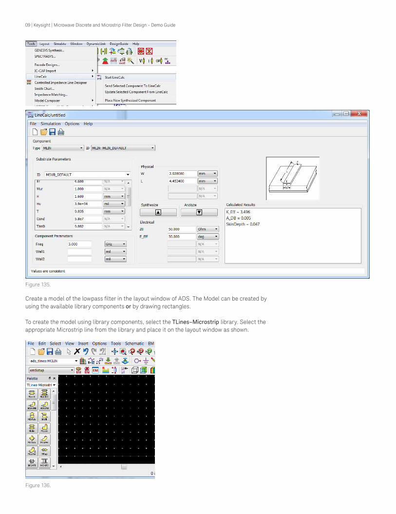
Calculate the length and width of the 50 Ω line using the line calc (Tools->Line Calc->Start Line Calc) window of ADS as shown in figure below.
50 Ω Line input & output connecting line:Width: 2.9 mm
Length: 4.5 mm
09 | Keysight | Microwave Discrete and Microstrip Filter Design - Demo Guide
Figure 135.
Figure 136.
Create a model of the lowpass filter in the layout window of ADS. The Model can be created by using the available library components or by drawing rectangles.
To create the model using library components, select the TLines–Microstrip library. Select the appropriate Microstrip line from the library and place it on the layout window as shown.

10 | Keysight | Microwave Discrete and Microstrip Filter Design - Demo Guide
Complete the model by connecting the transmission lines to form the stepped impedance lowpass filter as shown below based on the width & length calculations done earlier.
Figure 137.
Connect Pins at the input & output and define the substrate stackup and setup the EM simulation as described in the EM simulation chapter earlier. We shall use the following properties for the stackup:
Er=4.6Height = 4.6 mmLoss Tangent = 0.0023Metal Thickness = 0.035 mmMetal Conductivity = Cu (5.8E7 S/m)
In the EM setup window, go to Options > Mesh and turn on Edge Mesh.
Click the Simulate button and observe the S11 and S21 response.
Figure 138.

11 | Keysight | Microwave Discrete and Microstrip Filter Design - Demo Guide
It can be noted that the 3 dB cut-off has shifted to 1.68 GHz instead of 2 GHz as our theoretical calculations doesn’t allow accurate analysis of open end effect and a sudden impedance change in the transmission lines, hence the lengths of the lines needs to optimized to recover the desired 2 GHz cutoff frequency specifications.
This optimization can be carried out using the Momentum simulator in ADS or by performing a parametric sweep on the lengths of Capacitive and Inductive lines.
Parametric EM Simulations in ADSTo begin parametric simulation on the layout, we need to define the variable parameters that shall be associated with the layout components. Click EM > Component > Parameters as shown below.
Figure 139.
Figure 140.
12 | Keysight | Microwave Discrete and Microstrip Filter Design - Demo Guide
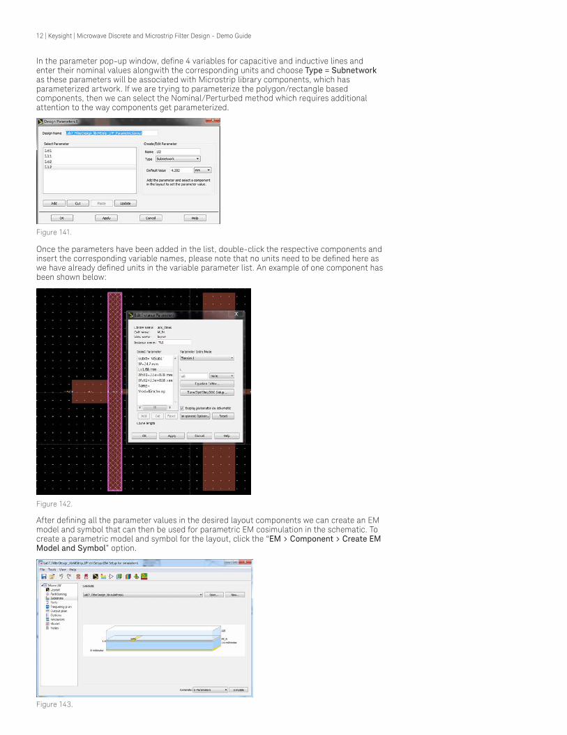
In the parameter pop-up window, define 4 variables for capacitive and inductive lines and enter their nominal values alongwith the corresponding units and choose Type = Subnetwork as these parameters will be associated with Microstrip library components, which has parameterized artwork. If we are trying to parameterize the polygon/rectangle based components, then we can select the Nominal/Perturbed method which requires additional attention to the way components get parameterized.
Figure 141.
Once the parameters have been added in the list, double-click the respective components and insert the corresponding variable names, please note that no units need to be defined here as we have already defined units in the variable parameter list. An example of one component has been shown below:
Figure 142.
Figure 143.
After defining all the parameter values in the desired layout components we can create an EM model and symbol that can then be used for parametric EM cosimulation in the schematic. To create a parametric model and symbol for the layout, click the “EM > Component > Create EM Model and Symbol” option.

13 | Keysight | Microwave Discrete and Microstrip Filter Design - Demo Guide
Figure 145.
Open a new schematic cell and drag and drop the emModel component to place it as subcircuit. You will notice the defined parameters being added to the emModel component, which can then be swept using the regular Parameter Sweep component in the ADS schematic as shown below. In this case, we have defined variables L1-L4 and assigned it to the emModel component. To start with, we sweep the length of L2 (1st inductive line) from 6.145 to 12.145 in steps of 1.
At this stage, we can decide to setup optimization and then optimize the layout component variables like any other circuit optimization, but please note that EM optimization will take longer as compared to circuit based optimization but produces more an accurate response as the EM simulation will be performed for every combination.
Figure 144.
Once done, observe the main ADS window where the name of the emmodel and symbol are displayed below the layout cell name as shown below:
14 | Keysight | Microwave Discrete and Microstrip Filter Design - Demo Guide
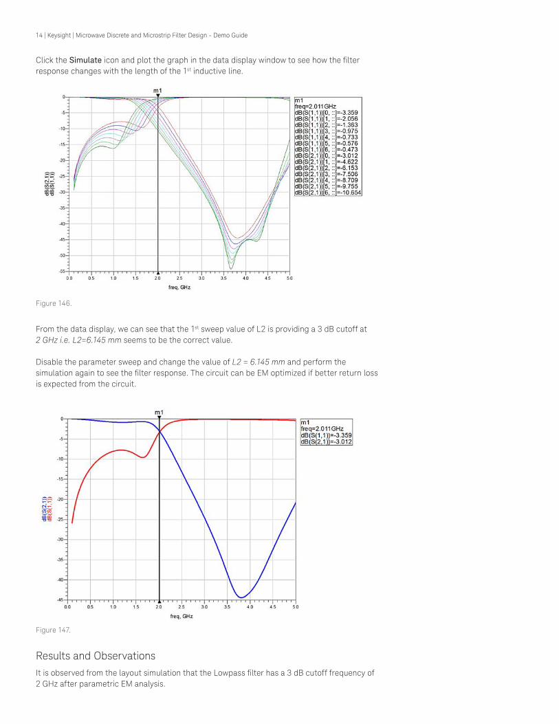
From the data display, we can see that the 1st sweep value of L2 is providing a 3 dB cutoff at 2 GHz i.e. L2=6.145 mm seems to be the correct value.
Disable the parameter sweep and change the value of L2 = 6.145 mm and perform the simulation again to see the filter response. The circuit can be EM optimized if better return loss is expected from the circuit.
Figure 147.
Results and ObservationsIt is observed from the layout simulation that the Lowpass filter has a 3 dB cutoff frequency of 2 GHz after parametric EM analysis.
Figure 146.
Click the Simulate icon and plot the graph in the data display window to see how the filter response changes with the length of the 1st inductive line.

15 | Keysight | Microwave Discrete and Microstrip Filter Design - Demo Guide
Typical DesignUpper Cutoff Frequency (fc1) : 1.9 GHzLower Cutoff Frequency (fc2) : 2.1 GHzRipple in passband : 0.5 dBOrder of the filter : 3
Type of Approximation : Chebyshev
Prototype values of the filterThe prototype values of the filter for a Chebyshev approximation is calculated using the formulae given above.
The prototype values for the given specifications of the filter areg1 = 1.5963, g2 = 1.0967 & g3 = 1.5963
Lumped model of the filterThe Lumped values of the Bandpass filter after frequency and impedance scaling are given by:
L’1 = L1Z0/ω 0 ∆
C’1= ∆ /L1Z0 ω 0
L’2 = ∆ Z0/ω 0 C2
C’2 = C2 /Z0 ∆ ω 0
L’3 = L3Z0/ω 0 ∆
C’3 = ∆ /L3Z0 ω 0 where, Z0 is 50 Ω
∆ = (ω2 – ω 1)/ω0
The resulting lumped values are given by:
L’1 = 63 nH
C’1= 0.1004 pF
L’2 = 0.365 nH
C’2 = 17.34 pF
L’3 = 63 nH
C’3 = 0.1004 pF
The Geometry of the lumped element bandpass filter is shown in the next figure.
Simulation of a Lumped and Distributed Bandpass Filter Using ADS

16 | Keysight | Microwave Discrete and Microstrip Filter Design - Demo Guide
Distributed Model of the FilterCalculate the value of j from the prototype values as follows:
Where, ∆ = (ω2 – ω1)/ω0
Z0 = Characteristic Impedance = 50 Ω
The values of odd and even mode impedances can be calculated as follows:
z0e = z0[1 + jz0 + ( jz0) 2 ]
z0o = z0[1 + jz0 + ( jz0) 2 ]
Figure 148.
⎥⎥⎥
⎦
⎤
⎢⎢⎢
⎣
⎡
=∆
1210 gjZ
π
nn ggnjZ120 −
∆= π For n =2, 3….N,
1210+
∆+ =
NN ggNjZ π
Schematic Simulation Steps for the Lumped Bandpass FilterOpen the Schematic window of ADS and construct the lumped bandpass filter as shown below. Setup the S-Parameter simulation from 1 GHz to 3 GHz with steps of 5 MHz (401 points).
Figure 149.

17 | Keysight | Microwave Discrete and Microstrip Filter Design - Demo Guide
Results and ObservationsIt is observed from the schematic simulation that the lumped model of the bandpass filter has an upper cutoff at 1.9 GHz, lower cutoff at 2.1 GHz and a roll off as per the specifications.
Layout Simulation Steps for the Distributed Bandpass FilterCalculate the odd mode and even mode impedance values (Zoo & Zoe) of the bandpass filter using the design procedure given above. Synthesize the physical parameters (length & width) for the coupled lines for a substrate thickness of 1.6 mm and dielectric constant of 4.6.
The physical parameters of the coupled lines for the given values of Zoo and Zoe are given as follows:
Substrate thickness: 1.6 mmDielectric constant: 4.6Frequency: 2 GHzElectrical length: 90 degrees
Section 1: Zoo = 36.23, Zoe = 66.65 Width = 2.545 Length = 20.52 Spacing = 0.409
Section 2: Zoo = 56.68, Zoe = 44.73 Width = 2.853 Length = 20.197 Spacing = 1.730
Figure 150.
Click the Simulate icon to observe the graph as illustrated:

18 | Keysight | Microwave Discrete and Microstrip Filter Design - Demo Guide
Calculate the length and width of the 50 Ω line using the linecalc window of ADS as done earlier.
– 50 Ω Line: – Width: 2.9 mm – Length: 5 mm
Create a model of the bandpass filter in the layout window of ADS. The Model can be created by using the available library components or by drawing rectangles.
To create the model using library components select the MCFIL from TLines–Microstrip library. Select the appropriate kind of Microstrip line from the library and place it on the layout window as shown in Figure 152.
Figure 151.
Section 3: Zoo = 56.68, Zoe = 44.73 Width = 2.853 Length = 20.197 Spacing = 1.730
Section 4: Zoo = 36.23, Zoe = 66.65 Width = 2.545 Length = 20.52 Spacing = 0.409
19 | Keysight | Microwave Discrete and Microstrip Filter Design - Demo Guide
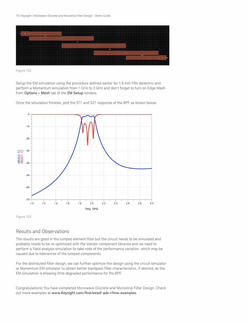
Setup the EM simulation using the procedure defined earlier for 1.6 mm FR4 dielectric and perform a Momentum simulation from 1 GHz to 3 GHz and don’t forget to turn on Edge Mesh from Options > Mesh tab of the EM Setup window.
Once the simulation finishes, plot the S11 and S21 response of the BPF as shown below:
Results and ObservationsThe results are good in the lumped element filter but the circuit needs to be simulated and probably needs to be re-optimized with the Vendor component libraries and we need to perform a Yield analysis simulation to take note of the performance variation, which may be caused due to tolerances of the lumped components.
For the distributed filter design, we can further optimize the design using the circuit simulator or Momentum EM simulator to obtain better bandpass filter characteristics, if desired, as the EM simulation is showing little degraded performance for fhs BPF.
Congratulations! You have completed Microwave Discrete and Microstrip Filter Design. Check out more examples at www.Keysight.com/find/eesof-ads-rfmw-examples.
Figure 153.
Figure 152.

20 | Keysight | Microwave Discrete and Microstrip Filter Design - Demo Guide
This information is subject to change without notice.© Keysight Technologies, 2016Published in USA, June 16, 20165992-1624ENwww.keysight.com
EvolvingOur unique combination of hardware, software, support, and people can help you reach your next breakthrough. We are unlocking the future of technology.
From Hewlett-Packard to Agilent to Keysight
myKeysightwww.keysight.com/find/mykeysightA personalized view into the information most relevant to you.
For more information on Keysight Technologies’ products, applications or services, please contact your local Keysight office. The complete list is available at:www.keysight.com/find/contactus
Americas Canada (877) 894 4414Brazil 55 11 3351 7010Mexico 001 800 254 2440United States (800) 829 4444
Asia PacificAustralia 1 800 629 485China 800 810 0189Hong Kong 800 938 693India 1 800 11 2626Japan 0120 (421) 345Korea 080 769 0800Malaysia 1 800 888 848Singapore 1 800 375 8100Taiwan 0800 047 866Other AP Countries (65) 6375 8100
Europe & Middle EastAustria 0800 001122Belgium 0800 58580Finland 0800 523252France 0805 980333Germany 0800 6270999Ireland 1800 832700Israel 1 809 343051Italy 800 599100Luxembourg +32 800 58580Netherlands 0800 0233200Russia 8800 5009286Spain 800 000154Sweden 0200 882255Switzerland 0800 805353
Opt. 1 (DE)Opt. 2 (FR)Opt. 3 (IT)
United Kingdom 0800 0260637
For other unlisted countries:www.keysight.com/find/contactus(BP-06-08-16)
Learn more at
www.keysight.com/find/software
Start with a 30-day free trial.
www.keysight.com/find/free_trials
Download your next insightKeysight software is downloadable
expertise. From first simulation through
first customer shipment, we deliver the
tools your team needs to accelerate from
data to information to actionable insight.
– Electronic design automation (EDA)
software
– Application software
– Programming environments
– Productivity software