Embed Size (px)
Citation preview
©2002 Fairchild Semiconductor Corporation
www.fairchildsemi.com
Rev.1.0.5
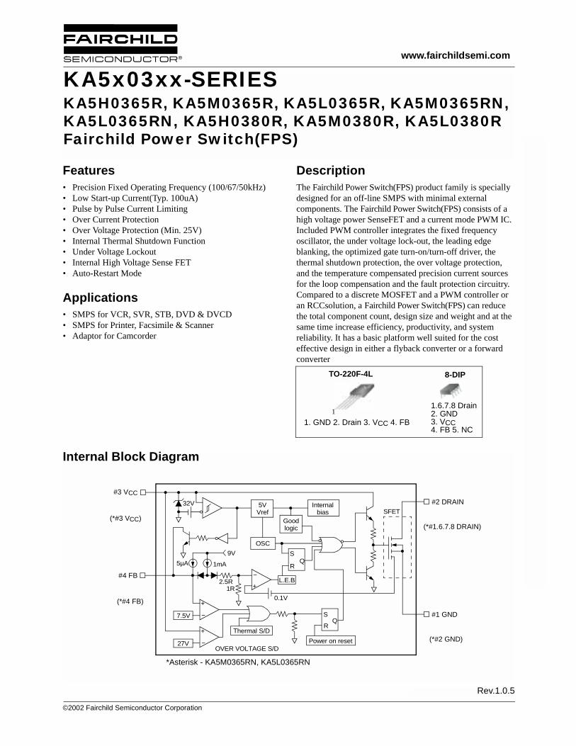
Features• Precision Fixed Operating Frequency (100/67/50kHz)• Low Start-up Current(Typ. 100uA)• Pulse by Pulse Current Limiting• Over Current Protection• Over Voltage Protection (Min. 25V)• Internal Thermal Shutdown Function• Under Voltage Lockout• Internal High Voltage Sense FET• Auto-Restart Mode
Applications• SMPS for VCR, SVR, STB, DVD & DVCD• SMPS for Printer, Facsimile & Scanner• Adaptor for Camcorder
DescriptionThe Fairchild Power Switch(FPS) product family is specially designed for an off-line SMPS with minimal external components. The Fairchild Power Switch(FPS) consists of a high voltage power SenseFET and a current mode PWM IC. Included PWM controller integrates the fixed frequency oscillator, the under voltage lock-out, the leading edge blanking, the optimized gate turn-on/turn-off driver, the thermal shutdown protection, the over voltage protection, and the temperature compensated precision current sources for the loop compensation and the fault protection circuitry. Compared to a discrete MOSFET and a PWM controller or an RCCsolution, a Fairchild Power Switch(FPS) can reduce the total component count, design size and weight and at the same time increase efficiency, productivity, and system reliability. It has a basic platform well suited for the cost effective design in either a flyback converter or a forward converter
Internal Block Diagram
#3 VCC32V
5µA9V
2.5R1R
1mA
0.1V+
−
OVER VOLTAGE S/D
+
−
7.5V
27V
Thermal S/D
S
RQ
Power on reset
+
−L.E.B
S
RQ
OSC
5VVref
Internalbias
Goodlogic
SFET#2 DRAIN
#1 GND
#4 FB
(*#3 VCC)
(*#4 FB)
(*#1.6.7.8 DRAIN)
(*#2 GND)
*Asterisk - KA5M0365RN, KA5L0365RN
KA5x03xx-SERIESKA5H0365R, KA5M0365R, KA5L0365R, KA5M0365RN, KA5L0365RN, KA5H0380R, KA5M0380R, KA5L0380R Fairchild Power Switch(FPS)
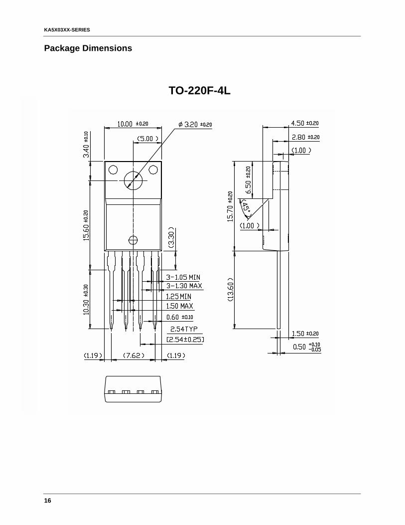
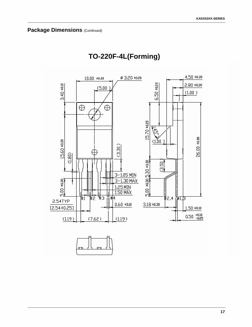
TO-220F-4L
1. GND 2. Drain 3. VCC 4. FB1
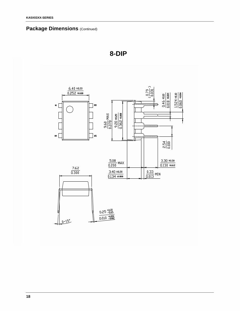
8-DIP
1.6.7.8 Drain2. GND3. VCC4. FB 5. NC
KA5X03XX-SERIES
2
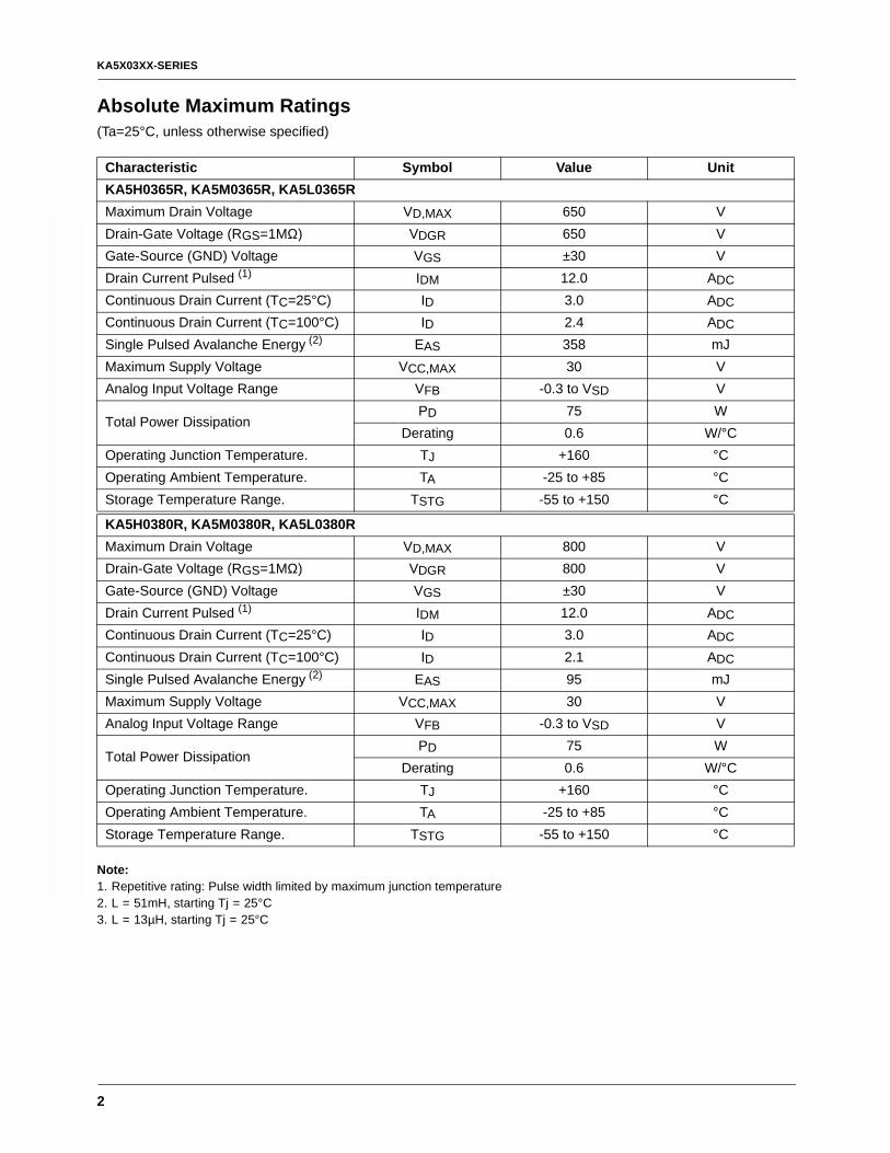
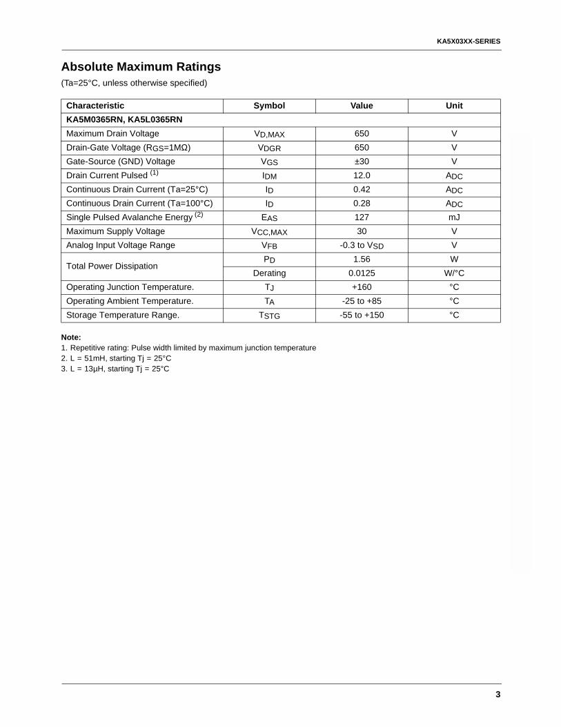
Absolute Maximum Ratings(Ta=25°C, unless otherwise specified)
Note:1. Repetitive rating: Pulse width limited by maximum junction temperature2. L = 51mH, starting Tj = 25°C3. L = 13µH, starting Tj = 25°C
Characteristic Symbol Value UnitKA5H0365R, KA5M0365R, KA5L0365RMaximum Drain Voltage VD,MAX 650 VDrain-Gate Voltage (RGS=1MΩ) VDGR 650 VGate-Source (GND) Voltage VGS ±30 VDrain Current Pulsed (1) IDM 12.0 ADCContinuous Drain Current (TC=25°C) ID 3.0 ADCContinuous Drain Current (TC=100°C) ID 2.4 ADCSingle Pulsed Avalanche Energy (2) EAS 358 mJMaximum Supply Voltage VCC,MAX 30 VAnalog Input Voltage Range VFB -0.3 to VSD V
Total Power DissipationPD 75 W
Derating 0.6 W/°COperating Junction Temperature. TJ +160 °COperating Ambient Temperature. TA -25 to +85 °CStorage Temperature Range. TSTG -55 to +150 °C
KA5H0380R, KA5M0380R, KA5L0380RMaximum Drain Voltage VD,MAX 800 VDrain-Gate Voltage (RGS=1MΩ) VDGR 800 VGate-Source (GND) Voltage VGS ±30 VDrain Current Pulsed (1) IDM 12.0 ADCContinuous Drain Current (TC=25°C) ID 3.0 ADCContinuous Drain Current (TC=100°C) ID 2.1 ADCSingle Pulsed Avalanche Energy (2) EAS 95 mJMaximum Supply Voltage VCC,MAX 30 VAnalog Input Voltage Range VFB -0.3 to VSD V
Total Power DissipationPD 75 W
Derating 0.6 W/°COperating Junction Temperature. TJ +160 °COperating Ambient Temperature. TA -25 to +85 °CStorage Temperature Range. TSTG -55 to +150 °C
KA5X03XX-SERIES
3
Absolute Maximum Ratings(Ta=25°C, unless otherwise specified)
Note:1. Repetitive rating: Pulse width limited by maximum junction temperature2. L = 51mH, starting Tj = 25°C3. L = 13µH, starting Tj = 25°C
Characteristic Symbol Value UnitKA5M0365RN, KA5L0365RNMaximum Drain Voltage VD,MAX 650 VDrain-Gate Voltage (RGS=1MΩ) VDGR 650 VGate-Source (GND) Voltage VGS ±30 VDrain Current Pulsed (1) IDM 12.0 ADCContinuous Drain Current (Ta=25°C) ID 0.42 ADCContinuous Drain Current (Ta=100°C) ID 0.28 ADCSingle Pulsed Avalanche Energy (2) EAS 127 mJMaximum Supply Voltage VCC,MAX 30 VAnalog Input Voltage Range VFB -0.3 to VSD V
Total Power DissipationPD 1.56 W
Derating 0.0125 W/°COperating Junction Temperature. TJ +160 °COperating Ambient Temperature. TA -25 to +85 °CStorage Temperature Range. TSTG -55 to +150 °C
KA5X03XX-SERIES
4
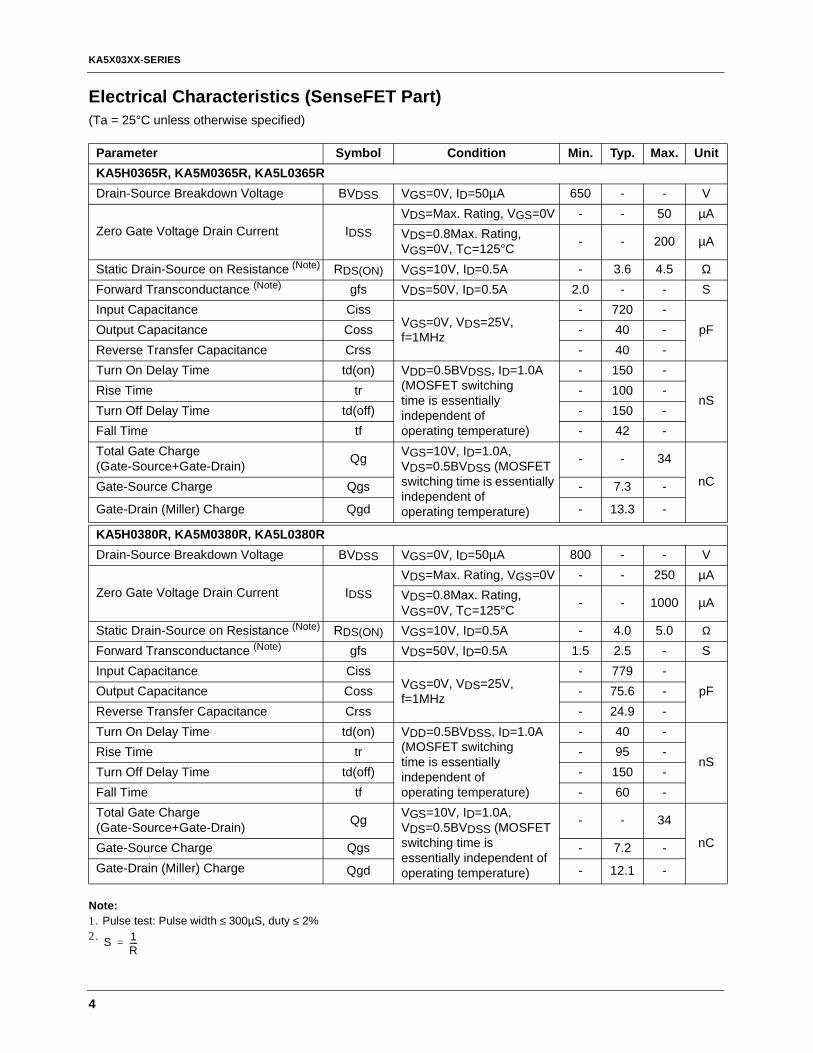
Electrical Characteristics (SenseFET Part)(Ta = 25°C unless otherwise specified)
Note:1. Pulse test: Pulse width ≤ 300µS, duty ≤ 2%2.
Parameter Symbol Condition Min. Typ. Max. UnitKA5H0365R, KA5M0365R, KA5L0365RDrain-Source Breakdown Voltage BVDSS VGS=0V, ID=50µA 650 - - V
Zero Gate Voltage Drain Current IDSSVDS=Max. Rating, VGS=0V - - 50 µAVDS=0.8Max. Rating,VGS=0V, TC=125°C - - 200 µA
Static Drain-Source on Resistance (Note) RDS(ON) VGS=10V, ID=0.5A - 3.6 4.5 ΩForward Transconductance (Note) gfs VDS=50V, ID=0.5A 2.0 - - SInput Capacitance Ciss
VGS=0V, VDS=25V,f=1MHz
- 720 -pFOutput Capacitance Coss - 40 -
Reverse Transfer Capacitance Crss - 40 -Turn On Delay Time td(on) VDD=0.5BVDSS, ID=1.0A
(MOSFET switchingtime is essentiallyindependent ofoperating temperature)
- 150 -
nSRise Time tr - 100 -Turn Off Delay Time td(off) - 150 -Fall Time tf - 42 -Total Gate Charge(Gate-Source+Gate-Drain) Qg VGS=10V, ID=1.0A,
VDS=0.5BVDSS (MOSFET switching time is essentially independent ofoperating temperature)
- - 34
nCGate-Source Charge Qgs - 7.3 -
Gate-Drain (Miller) Charge Qgd - 13.3 -
KA5H0380R, KA5M0380R, KA5L0380RDrain-Source Breakdown Voltage BVDSS VGS=0V, ID=50µA 800 - - V
Zero Gate Voltage Drain Current IDSSVDS=Max. Rating, VGS=0V - - 250 µAVDS=0.8Max. Rating,VGS=0V, TC=125°C - - 1000 µA
Static Drain-Source on Resistance (Note) RDS(ON) VGS=10V, ID=0.5A - 4.0 5.0 Ω
Forward Transconductance (Note) gfs VDS=50V, ID=0.5A 1.5 2.5 - SInput Capacitance Ciss
VGS=0V, VDS=25V,f=1MHz
- 779 -pFOutput Capacitance Coss - 75.6 -
Reverse Transfer Capacitance Crss - 24.9 -Turn On Delay Time td(on) VDD=0.5BVDSS, ID=1.0A
(MOSFET switchingtime is essentiallyindependent ofoperating temperature)
- 40 -
nSRise Time tr - 95 -Turn Off Delay Time td(off) - 150 -Fall Time tf - 60 -Total Gate Charge(Gate-Source+Gate-Drain) Qg VGS=10V, ID=1.0A,
VDS=0.5BVDSS (MOSFET switching time is essentially independent ofoperating temperature)
- - 34
nCGate-Source Charge Qgs - 7.2 -Gate-Drain (Miller) Charge Qgd - 12.1 -
S 1R----=
KA5X03XX-SERIES
5
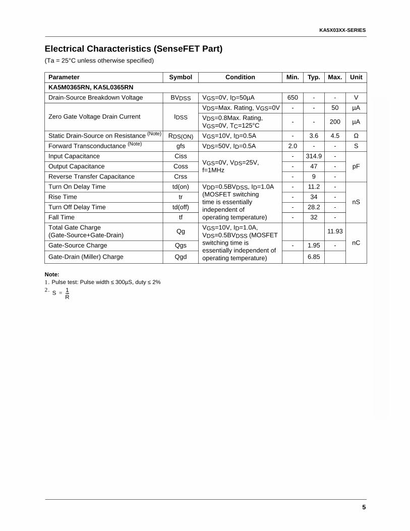
Electrical Characteristics (SenseFET Part)(Ta = 25°C unless otherwise specified)
Note:1. Pulse test: Pulse width ≤ 300µS, duty ≤ 2%2.
Parameter Symbol Condition Min. Typ. Max. UnitKA5M0365RN, KA5L0365RNDrain-Source Breakdown Voltage BVDSS VGS=0V, ID=50µA 650 - - V
Zero Gate Voltage Drain Current IDSSVDS=Max. Rating, VGS=0V - - 50 µAVDS=0.8Max. Rating,VGS=0V, TC=125°C - - 200 µA
Static Drain-Source on Resistance (Note) RDS(ON) VGS=10V, ID=0.5A - 3.6 4.5 ΩForward Transconductance (Note) gfs VDS=50V, ID=0.5A 2.0 - - SInput Capacitance Ciss
VGS=0V, VDS=25V,f=1MHz
- 314.9 -pFOutput Capacitance Coss - 47 -
Reverse Transfer Capacitance Crss - 9 -Turn On Delay Time td(on) VDD=0.5BVDSS, ID=1.0A
(MOSFET switchingtime is essentiallyindependent ofoperating temperature)
- 11.2 -
nSRise Time tr - 34 -Turn Off Delay Time td(off) - 28.2 -Fall Time tf - 32 -Total Gate Charge(Gate-Source+Gate-Drain) Qg VGS=10V, ID=1.0A,
VDS=0.5BVDSS (MOSFET switching time is essentially independent ofoperating temperature)
11.93
nCGate-Source Charge Qgs - 1.95 -
Gate-Drain (Miller) Charge Qgd 6.85
S 1R----=
KA5X03XX-SERIES
6
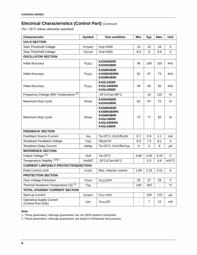
Electrical Characteristics (Control Part) (Continued)
(Ta = 25°C unless otherwise specified)
Note:1. These parameters, although guaranteed, are not 100% tested in production2. These parameters, although guaranteed, are tested in EDS(water test) process
Characteristic Symbol Test condition Min. Typ. Max. UnitUVLO SECTIONStart Threshold Voltage VSTART VFB=GND 14 15 16 VStop Threshold Voltage VSTOP VFB=GND 8.4 9 9.6 VOSCILLATOR SECTION
Initial Accuracy FOSCKA5H0365RKA5H0380R 90 100 110 kHz
Initial Accuracy FOSCKA5M0365RKA5M0365RNKA5M0380R
61 67 73 kHz
Initial Accuracy FOSCKA5L0365RKA5L0365RNKA5L0380R
45 50 55 kHz
Frequency Change With Temperature (2) - -25°C≤Ta≤+85°C - ±5 ±10 %
Maximum Duty Cycle Dmax KA5H0365RKA5H0380R 62 67 72 %
Maximum Duty Cycle Dmax
KA5M0365RKA5M0365RNKA5M0380RKA5L0365RKA5L0365RNKA5L0380R
72 77 82 %
FEEDBACK SECTIONFeedback Source Current IFB Ta=25°C, 0V<Vfb<3V 0.7 0.9 1.1 mAShutdown Feedback Voltage VSD Vfb>6.5V 6.9 7.5 8.1 VShutdown Delay Current Idelay Ta=25°C, 5V≤Vfb≤VSD 4 5 6 µAREFERENCE SECTIONOutput Voltage (1) Vref Ta=25°C 4.80 5.00 5.20 VTemperature Stability (1)(2) Vref/∆T -25°C≤Ta≤+85°C - 0.3 0.6 mV/°CCURRENT LIMIT(SELF-PROTECTION)SECTIONPeak Current Limit IOVER Max. inductor current 1.89 2.15 2.41 APROTECTION SECTIONOver Voltage Protection VOVP VCC>24V 25 27 29 VThermal Shutdown Temperature (Tj) (1) TSD - 140 160 - °CTOTAL STANDBY CURRENT SECTIONStart-up Current ISTART VCC=14V - 100 170 µAOperating Supply Current(Control Part Only) IOP VCC<28 - 7 12 mA
KA5X03XX-SERIES
7
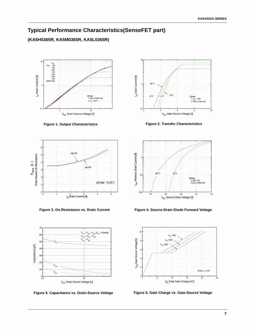
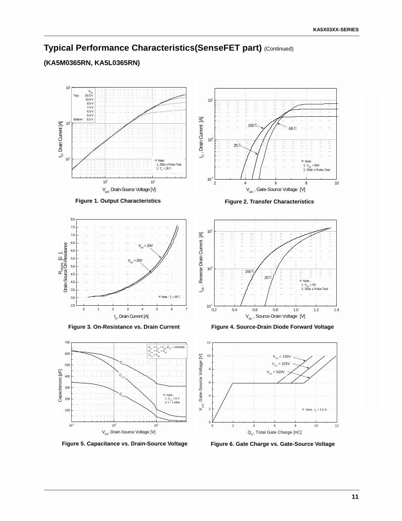
Typical Performance Characteristics(SenseFET part)(KA5H0365R, KA5M0365R, KA5L0365R)
1 100.1
1
10
@Notes: 1. 300 µs Pulse Test 2. TC = 25 oC
VGSTop : 15V 10V 8.0V 7.0V 6.0V 5.5V 5.0VBottom:4.5V
I D, D
rain
Cur
rent
[A]
VDS, Drain-Source Voltage [V]2 4 6 8 10
0.1
1
10
@Notes: 1. VDS = 30V 2. 300 µs Pulse Test
-25oC25 oC
150 oC
I D, D
rain
Cur
rent
[A]
VGS, Gate-Source Voltage [V]
0 1 2 3 4 50
1
2
3
4
5
6
7
@ Note : Tj=25
Vgs=10V
Vgs=20V
R DS(
on) ,
[Ω]
Drai
n-So
urce
On-
Resi
stanc
e
ID,Drain Current [A]0.4 0.6 0.8 1.0 1.2
0.01
0.1
1
@Notes : 1. VGS = 0 V 2. 300 µs Pulse Test
25 oC150 oC
I DR, R
ever
se D
rain
Cur
rent
[A]
VSD, Source-Drain Voltage [V]
100 1010
100
200
300
400
500
600
700
Crss
Coss
Ciss
Ciss = Cgs + Cgd (Cds = shorted)Coss = Cds + CgdCrss = Cgd
Capa
cita
nce
[pF]
VDS, Drain-Source Voltage [V]0 5 10 15 20 25
0
2
4
6
8
10
VDS=520V
VDS=320V
VDS=130V
@ Note : ID=3.0A
V GS,G
ate-
Sour
ce V
olta
ge[V
]
QG,Total Gate Charge [nC]
Figure 1. Output Characteristics Figure 2. Transfer Characteristics
Figure 3. On-Resistance vs. Drain Current Figure 4. Source-Drain Diode Forward Voltage
Figure 5. Capacitance vs. Drain-Source Voltage Figure 6. Gate Charge vs. Gate-Source Voltage
KA5X03XX-SERIES
8
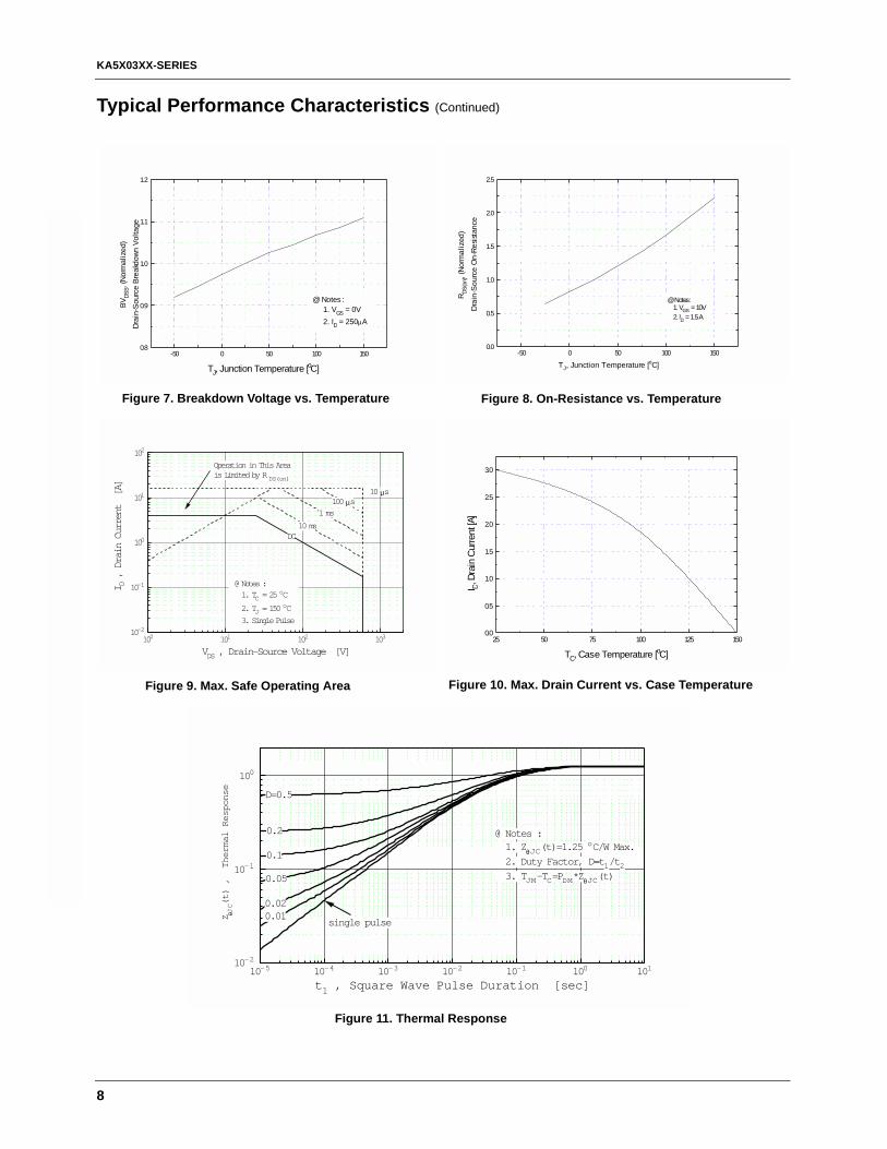
Typical Performance Characteristics (Continued)
-50 0 50 100 1500.8
0.9
1.0
1.1
1.2
@ Notes : 1. VGS = 0V 2. ID = 250µA
TJ, Junction Temperature [oC]
BVDS
S, (N
orm
aliz
ed)
Drai
n-So
urce
Bre
akdo
wn V
olta
ge
-50 0 50 100 1500.0
0.5
1.0
1.5
2.0
2.5
@ Notes: 1. VGS = 10V 2. ID = 1.5 A
TJ, Junction Temperature [oC]
R DS(o
n), (N
orm
aliz
ed)
Drai
n-So
urce
On-
Resis
tanc
e
100 101 102 10310-2
10-1
100
101
102
10 µs
DC
100 µs1 ms
10 ms
@ Notes : 1. TC = 25
oC
2. TJ = 150 oC
3. Single Pulse
Operation in This Area is Limited by R DS(on)
I D , Drain Current [A]
VDS , Drain-Source Voltage [V]25 50 75 100 125 150
0.0
0.5
1.0
1.5
2.0
2.5
3.0I D,
Dra
in C
urre
nt [A
]
TC, Case Temperature [oC]
10-5 10-4 10-3 10-2 10-1 100 10110-2
10-1
100
single pulse
0.2
0.1
0.010.02
0.05
D=0.5
@ Notes : 1. Z
θJC(t)=1.25 oC/W Max.
2. Duty Factor, D=t1/t2 3. TJM-TC=PDM*ZθJC(t)
Z θJC(t) , Thermal Response
t1 , Square Wave Pulse Duration [sec]
Figure 7. Breakdown Voltage vs. Temperature Figure 8. On-Resistance vs. Temperature
Figure 9. Max. Safe Operating Area Figure 10. Max. Drain Current vs. Case Temperature
Figure 11. Thermal Response
KA5X03XX-SERIES
9
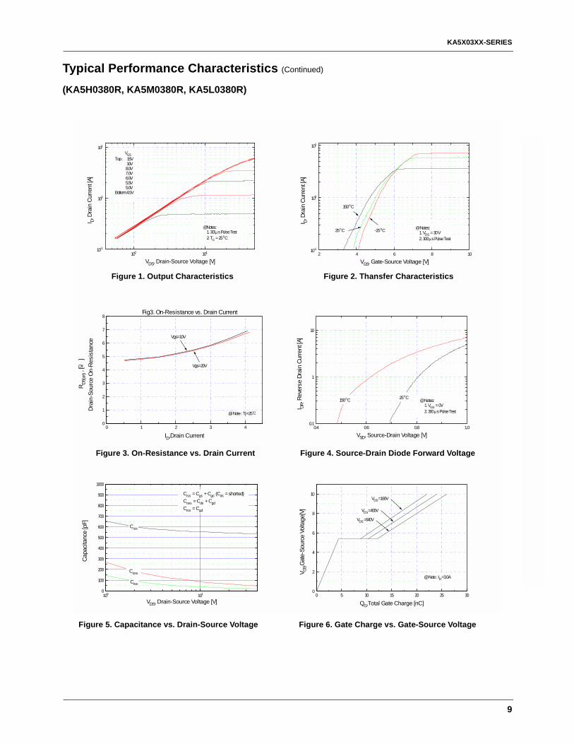
Typical Performance Characteristics (Continued)
(KA5H0380R, KA5M0380R, KA5L0380R)
100 10110-1
100
101
@Notes: 1. 300µs Pulse Test 2. TC = 25 oC
VGSTop : 15V 10V 8.0V 7.0V 6.0V 5.5V 5.0VBottom:4.5V
I D, Dr
ain
Curre
nt [A
]
VDS, Drain-Source Voltage [V]2 4 6 8 10
10-1
100
101
@ Notes: 1. VDS = 30 V 2. 300 µs Pulse Test
-25 oC25 oC
150 oC
I D, D
rain
Cur
rent
[A]
VGS, Gate-Source Voltage [V]
0.4 0.6 0.8 1.00.1
1
10
@ Notes: 1. VGS = 0V 2. 300 µs Pulse Test
25 oC150 oC
I DR, R
ever
se D
rain
Cur
rent
[A]
VSD, Source-Drain Voltage [V]
100 1010
100
200
300
400
500
600
700
800
900
1000
Crss
Coss
Ciss
Ciss = Cgs + Cgd (Cds = shorted)Coss = Cds + CgdCrss = Cgd
Capa
citan
ce [p
F]
VDS, Drain-Source Voltage [V]0 5 10 15 20 25 30
0
2
4
6
8
10
@ Note : ID=3.0A
VDS=640V
VDS=400V
VDS=160V
V GS,G
ate-
Sour
ce V
olta
ge[V
]
QG,Total Gate Charge [nC]
0 1 2 3 40
1
2
3
4
5
6
7
8
Vgs=10V
Vgs=20V
@ Note : Tj=25
Fig3. On-Resistance vs. Drain Current
R DS(o
n) ,
[Ω]
Dra
in-S
ourc
e On
-Res
ista
nce
ID,Drain Current
Figure 1. Output Characteristics Figure 2. Thansfer Characteristics
Figure 3. On-Resistance vs. Drain Current Figure 4. Source-Drain Diode Forward Voltage
Figure 5. Capacitance vs. Drain-Source Voltage Figure 6. Gate Charge vs. Gate-Source Voltage
KA5X03XX-SERIES
10
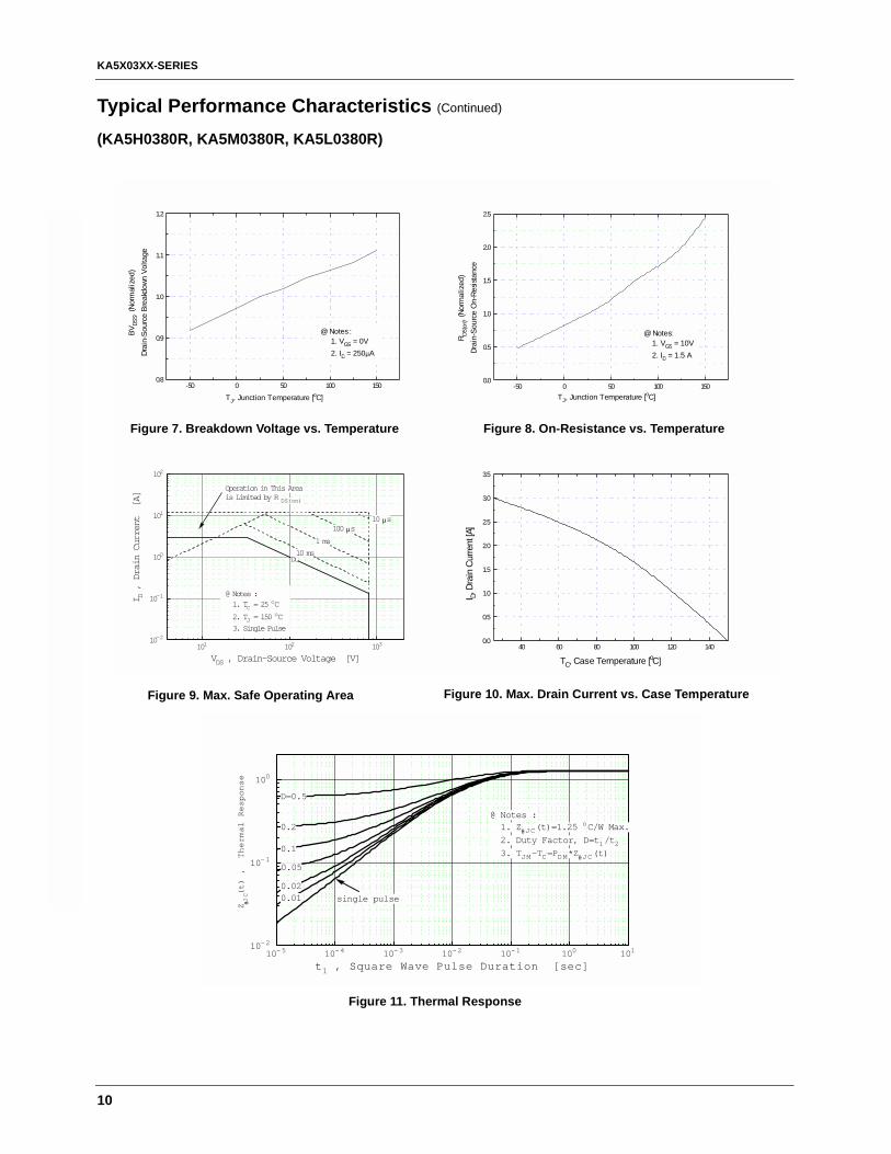
Typical Performance Characteristics (Continued)
(KA5H0380R, KA5M0380R, KA5L0380R)
10-5 10-4 10-3 10-2 10-1 100 10110-2
10-1
100
single pulse
0.2
0.1
0.010.02
0.05
D=0.5
@ Notes : 1. ZθJC(t)=1.25
oC/W Max.
2. Duty Factor, D=t1/t2 3. TJM-TC=PDM*ZθJC(t)
Z θJC(t) , Thermal Response
t1 , Square Wave Pulse Duration [sec]
-50 0 50 100 1500.8
0.9
1.0
1.1
1.2
@ Notes : 1. VGS = 0V 2. ID = 250µA
TJ, Junction Temperature [oC]
BVDS
S, (N
orm
aliz
ed)
Drai
n-So
urce
Bre
akdo
wn V
olta
ge
-50 0 50 100 1500.0
0.5
1.0
1.5
2.0
2.5
R DS(o
n), (N
orm
aliz
ed)
Drai
n-So
urce
On-
Resis
tanc
e
TJ, Junction Temperature [oC]
@ Notes: 1. VGS = 10V 2. ID = 1.5 A
101 102 10310-2
10-1
100
101
102
100 µs
DC
10 µs
1 ms
10 ms
@ Notes : 1. TC = 25
oC
2. TJ = 150 oC
3. Single Pulse
Operation in This Area is Limited by R DS(on)
I D , Drain Current [A]
VDS , Drain-Source Voltage [V]40 60 80 100 120 140
0.0
0.5
1.0
1.5
2.0
2.5
3.0
3.5I D,
Dra
in C
urre
nt [A
]
TC, Case Temperature [oC]
Figure 7. Breakdown Voltage vs. Temperature Figure 8. On-Resistance vs. Temperature
Figure 9. Max. Safe Operating Area Figure 10. Max. Drain Current vs. Case Temperature
Figure 11. Thermal Response
KA5X03XX-SERIES
11
Typical Performance Characteristics(SenseFET part) (Continued)
(KA5M0365RN, KA5L0365RN)
100 101
10-1
100
101
VGSTop : 15.0 V 10.0 V 8.0 V 7.0 V 6.5 V 6.0 VBottom : 5.5 V
※ Note : 1. 250μ s Pulse Test 2. TC = 25
I D, D
rain
Curre
nt [A
]
VDS, Drain-Source Voltage [V]2 4 6 8 10
10-1
100
101
※ Note 1. VDS = 50V 2. 250μ s Pulse Test
-55150
25
I D , D
rain
Cur
rent
[A]
VGS , Gate-Source Voltage [V]
0 1 2 3 4 5 6 72.5
3.0
3.5
4.0
4.5
5.0
5.5
6.0
6.5
7.0
7.5
8.0
VGS
= 20V
VGS = 10V
※ Note : TJ = 25
RDS
(ON)
[Ω],
Drain
-Sou
rce
On-R
esist
ance
ID, Drain Current [A]0.2 0.4 0.6 0.8 1.0 1.2 1.4
10-1
100
101
25150
※ Note : 1. VGS = 0V 2. 250μ s Pulse TestI DR
, Re
vers
e Dr
ain
Curre
nt [
A]
VSD
, Source-Drain Voltage [V]
10-1 100 101
100
200
300
400
500
600
700Ciss = Cgs + Cgd (Cds = shorted)C
oss = C
ds + C
gdCrss = Cgd
※ Note ; 1. V
GS = 0 V
2. f = 1 MHz
Crss
Coss
Ciss
Cap
acita
nces
[pF]
VDS, Drain-Source Voltage [V]0 2 4 6 8 10 12
0
2
4
6
8
10
12
VDS
= 325V
VDS = 130V
VDS = 520V
※ Note : ID = 3.0 A
V GS, G
ate-
Sou
rce
Vol
tage
[V]
QG, Total Gate Charge [nC]
Figure 1. Output Characteristics Figure 2. Transfer Characteristics
Figure 3. On-Resistance vs. Drain Current Figure 4. Source-Drain Diode Forward Voltage
Figure 5. Capacitance vs. Drain-Source Voltage Figure 6. Gate Charge vs. Gate-Source Voltage
KA5X03XX-SERIES
12
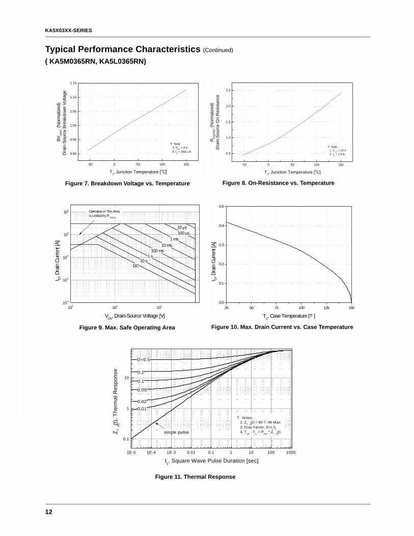
Typical Performance Characteristics (Continued)
( KA5M0365RN, KA5L0365RN)
-50 0 50 100 150
0.90
0.95
1.00
1.05
1.10
1.15
※ Note : 1. V
GS = 0 V
2. ID = 250 μ A
BVD
SS, (
Nor
mal
ized)
Drai
n-So
urce
Bre
akdo
wn V
olta
ge
TJ, Junction Temperature [oC]
-50 0 50 100 150
0.5
1.0
1.5
2.0
2.5
※ Note : 1. V
GS = 10 V
2. ID = 1.5 A
RD
S(O
N),
(Nor
mal
ized
)D
rain
-Sou
rce
On-
Res
ista
nce
TJ, Junction Temperature [oC]
Figure 7. Breakdown Voltage vs. Temperature Figure 8. On-Resistance vs. Temperature
Figure 9. Max. Safe Operating Area Figure 10. Max. Drain Current vs. Case Temperature
Figure 11. Thermal Response
100 101 10210-3
10-2
10-1
100
101
DC10 s
1 s100 ms
10 ms1 ms
100 µs10 µs
Operation in This Area is Limited by R DS(on)
I D, D
rain
Curre
nt [A
]
VDS, Drain-Source Voltage [V]25 50 75 100 125 150
0.0
0.1
0.2
0.3
0.4
0.5
I D, D
rain
Curre
nt [A
]
TC, Case Temperature [? ]
1E-5 1E-4 1E-3 0.01 0.1 1 10 100 1000
0.1
1
10
0.05
0.020.01
single pulse
0.2
0.1
D=0.5
? Notes : 1. Z
? JC(t) = 80 ? /W Max.
2. Duty Factor, D=t1/t2 3. T
JM - T
C = P
DM * Z
? JC(t)
Z ?JC(t)
, The
rmal
Res
pons
e
t1, Square Wave Pulse Duration [sec]
KA5X03XX-SERIES
13
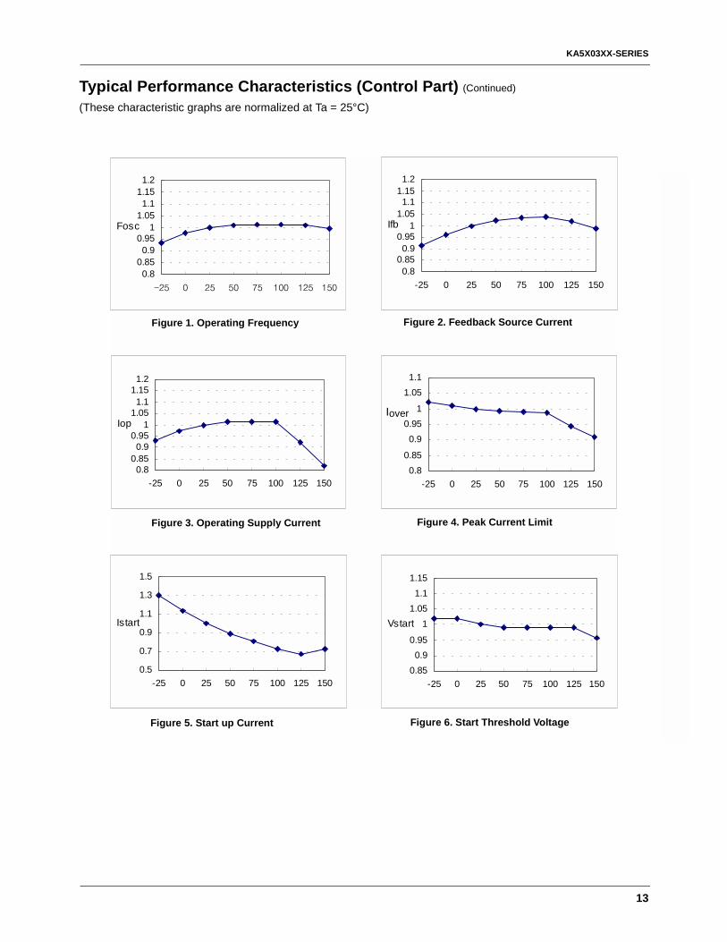
Typical Performance Characteristics (Control Part) (Continued)
(These characteristic graphs are normalized at Ta = 25°C)
Fig.1 Operating Frequency
0.80.850.9
0.951
1.051.1
1.151.2
-25 0 25 50 75 100 125 150
Fosc
Fig.2 Feedback Source Current
0.80.850.9
0.951
1.051.1
1.151.2
-25 0 25 50 75 100 125 150
Ifb
Fig.3 Operating Current
0.80.850.9
0.951
1.051.1
1.151.2
-25 0 25 50 75 100 125 150
Iop
Fig.4 Max Inductor Current
0.80.85
0.90.95
1
1.051.1
-25 0 25 50 75 100 125 150
Ipeak
Fig.5 Start up Current
0.5
0.7
0.9
1.1
1.3
1.5
-25 0 25 50 75 100 125 150
Istart
Fig.6 Start Threshold Voltage
0.850.9
0.95
11.051.1
1.15
-25 0 25 50 75 100 125 150
Vstart
Figure 1. Operating Frequency Figure 2. Feedback Source Current
Figure 3. Operating Supply Current Figure 4. Peak Current Limit
Figure 5. Start up Current Figure 6. Start Threshold Voltage
Iover
KA5X03XX-SERIES
14
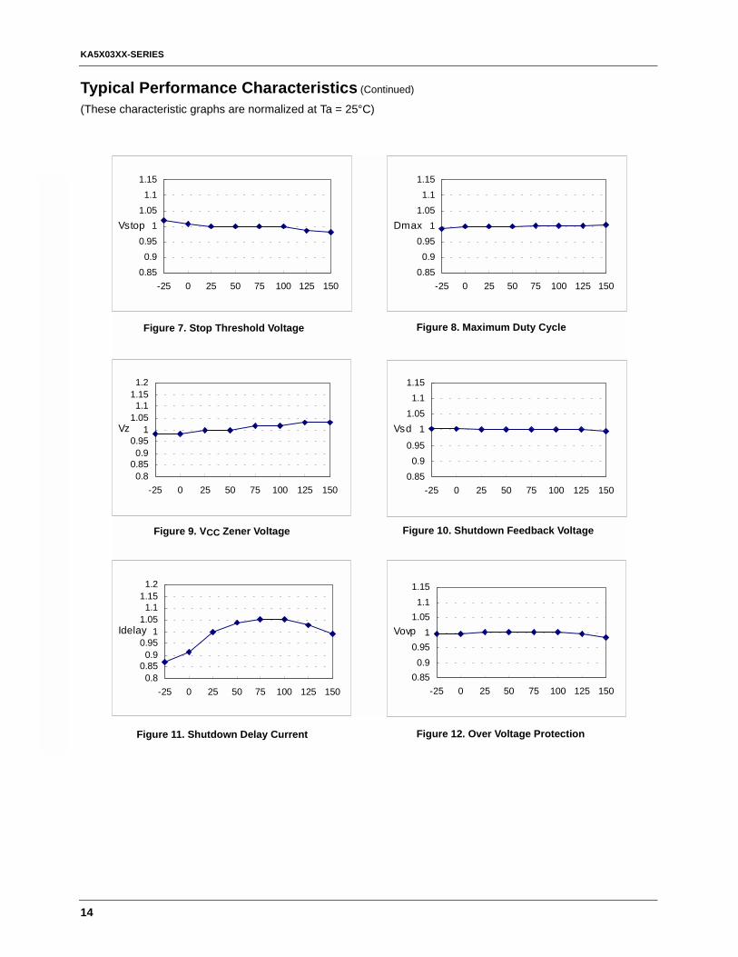
Typical Performance Characteristics (Continued)
(These characteristic graphs are normalized at Ta = 25°C)
Fig.7 Stop Threshold Voltage
0.850.9
0.951
1.051.1
1.15
-25 0 25 50 75 100 125 150
Vstop
Fig.8 Maximum Duty Cycle
0.850.9
0.951
1.051.1
1.15
-25 0 25 50 75 100 125 150
Dmax
Fig.9 Vcc Zener Voltage
0.80.850.9
0.951
1.051.1
1.151.2
-25 0 25 50 75 100 125 150
Vz
Fig.10 Shutdown Feedback Voltage
0.850.9
0.95
11.051.1
1.15
-25 0 25 50 75 100 125 150
Vsd
Fig.11 Shutdown Delay Current
0.80.850.9
0.951
1.051.1
1.151.2
-25 0 25 50 75 100 125 150
Idelay
Fig.12 Over Voltage Protection
0.850.9
0.951
1.051.1
1.15
-25 0 25 50 75 100 125 150
Vovp
Figure 7. Stop Threshold Voltage Figure 8. Maximum Duty Cycle
Figure 9. VCC Zener Voltage Figure 10. Shutdown Feedback Voltage
Figure 11. Shutdown Delay Current Figure 12. Over Voltage Protection
KA5X03XX-SERIES
15
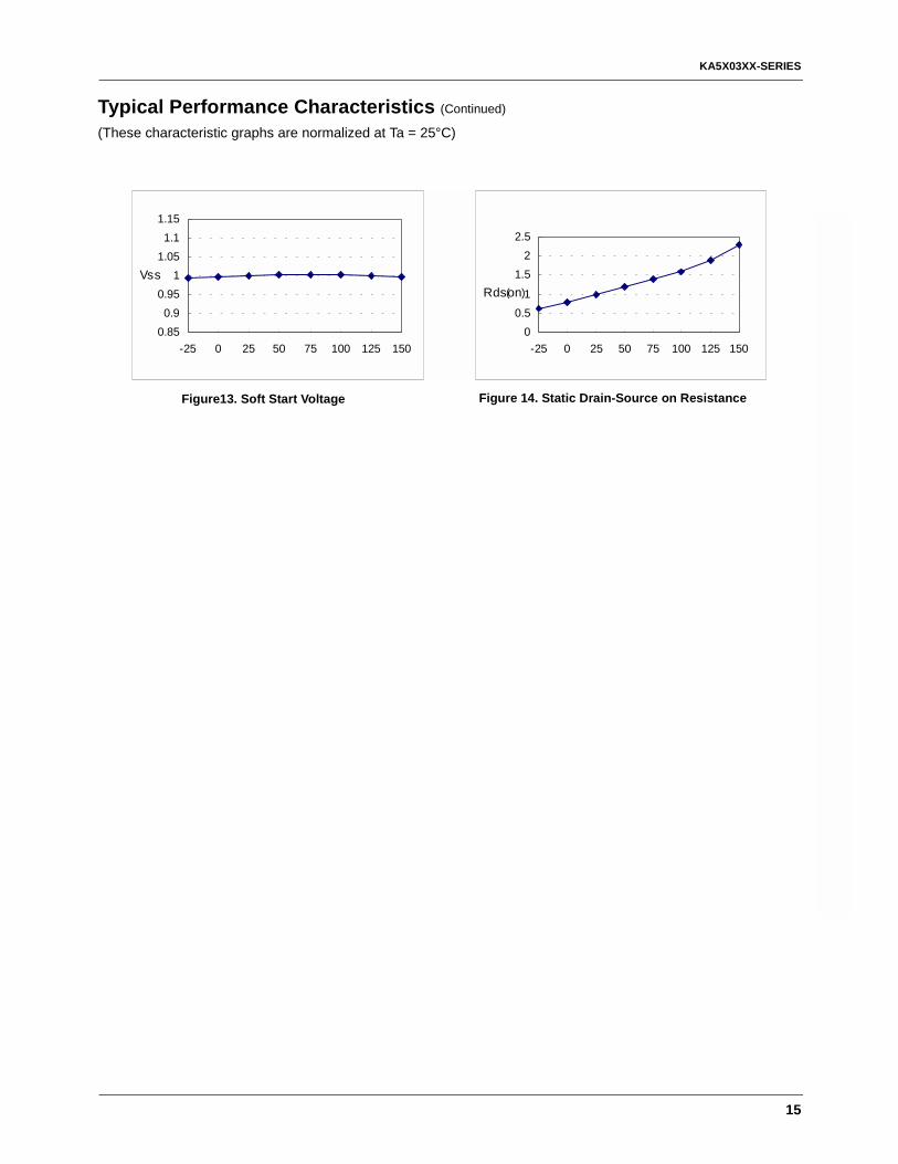
Typical Performance Characteristics (Continued)
(These characteristic graphs are normalized at Ta = 25°C)
Figure13. Soft Start Voltage Figure 14. Static Drain-Source on Resistance
Fig.13 Soft Start Voltage
0.850.9
0.951
1.051.1
1.15
-25 0 25 50 75 100 125 150
Vss
Fig.14 Drain Source Turn-onResistance
00.5
1
1.52
2.5
-25 0 25 50 75 100 125 150
Rdson
( )
KA5X03XX-SERIES
16
Package Dimensions
TO-220F-4L
KA5X03XX-SERIES
17
Package Dimensions (Continued)
TO-220F-4L(Forming)
KA5X03XX-SERIES
18
Package Dimensions (Continued)
8-DIP
KA5X03XX-SERIES
19
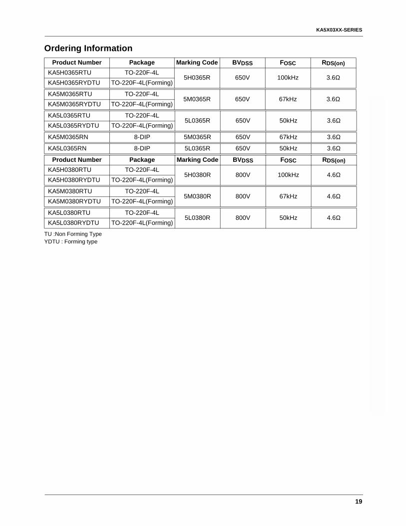
Ordering Information
TU :Non Forming TypeYDTU : Forming type
Product Number Package Marking Code BVDSS FOSC RDS(on)KA5H0365RTU TO-220F-4L
5H0365R 650V 100kHz 3.6ΩKA5H0365RYDTU TO-220F-4L(Forming)
KA5M0365RTU TO-220F-4L5M0365R 650V 67kHz 3.6Ω
KA5M0365RYDTU TO-220F-4L(Forming)
KA5L0365RTU TO-220F-4L5L0365R 650V 50kHz 3.6Ω
KA5L0365RYDTU TO-220F-4L(Forming)
KA5M0365RN 8-DIP 5M0365R 650V 67kHz 3.6Ω
KA5L0365RN 8-DIP 5L0365R 650V 50kHz 3.6Ω
Product Number Package Marking Code BVDSS FOSC RDS(on)KA5H0380RTU TO-220F-4L
5H0380R 800V 100kHz 4.6ΩKA5H0380RYDTU TO-220F-4L(Forming)
KA5M0380RTU TO-220F-4L5M0380R 800V 67kHz 4.6Ω
KA5M0380RYDTU TO-220F-4L(Forming)
KA5L0380RTU TO-220F-4L5L0380R 800V 50kHz 4.6Ω
KA5L0380RYDTU TO-220F-4L(Forming)
KA5X03XX-SERIES
12/12/02 0.0m 001Stock#DSxxxxxxxx
2002 Fairchild Semiconductor Corporation
LIFE SUPPORT POLICY FAIRCHILD’S PRODUCTS ARE NOT AUTHORIZED FOR USE AS CRITICAL COMPONENTS IN LIFE SUPPORT DEVICES OR SYSTEMS WITHOUT THE EXPRESS WRITTEN APPROVAL OF THE PRESIDENT OF FAIRCHILD SEMICONDUCTOR CORPORATION. As used herein:
1. Life support devices or systems are devices or systems which, (a) are intended for surgical implant into the body, or (b) support or sustain life, and (c) whose failure to perform when properly used in accordance with instructions for use provided in the labeling, can be reasonably expected to result in a significant injury of the user.
2. A critical component in any component of a life support device or system whose failure to perform can be reasonably expected to cause the failure of the life support device or system, or to affect its safety or effectiveness.
www.fairchildsemi.com
DISCLAIMERFAIRCHILD SEMICONDUCTOR RESERVES THE RIGHT TO MAKE CHANGES WITHOUT FURTHER NOTICE TO ANY PRODUCTS HEREIN TO IMPROVE RELIABILITY, FUNCTION OR DESIGN. FAIRCHILD DOES NOT ASSUME ANY LIABILITY ARISING OUT OF THE APPLICATION OR USE OF ANY PRODUCT OR CIRCUIT DESCRIBED HEREIN; NEITHER DOES IT CONVEY ANY LICENSE UNDER ITS PATENT RIGHTS, NOR THE RIGHTS OF OTHERS.


![Crow Search Optimized Control of Photovoltaic …A DC -DC converter [6], buck boost converter [7], Luo converter [8], canonical switching cell (CSC) converter [9], zeta converter [10]](https://img.pdfslide.us/doc/110x75/5fcf5114fee703425c72d389/crow-search-optimized-control-of-photovoltaic-a-dc-dc-converter-6-buck-boost.jpg)


![Torque Converter Voith Torque Converter[1]](https://img.pdfslide.us/doc/110x75/55cf992e550346d0339c0bc5/torque-converter-voith-torque-converter1.jpg)