Embed Size (px)
Citation preview
MAINTENANCE MANUAL
KA 51BSLAVING ACCESSORY
MANUAL NUMBER 006-15627-0007REVISION 7 AUGUST, 2001
WARNINGPrior to the export of this document, review for export license requirement is needed.
COPYRIGHT NOTICE
©1975-2001 Honeywell International Inc.
Reproduction of this publication or any portion thereof by any means without the express written permission of Honeywell is prohibited. For further information contact the manager, Technical Publications, Honeywell, One Technology Center, 23500 West 105th Street Olathe KS 66061 telephone: (913) 712-0400.
MAINTENANCE MANUAL
KA 51BSLAVING ACCESSORY
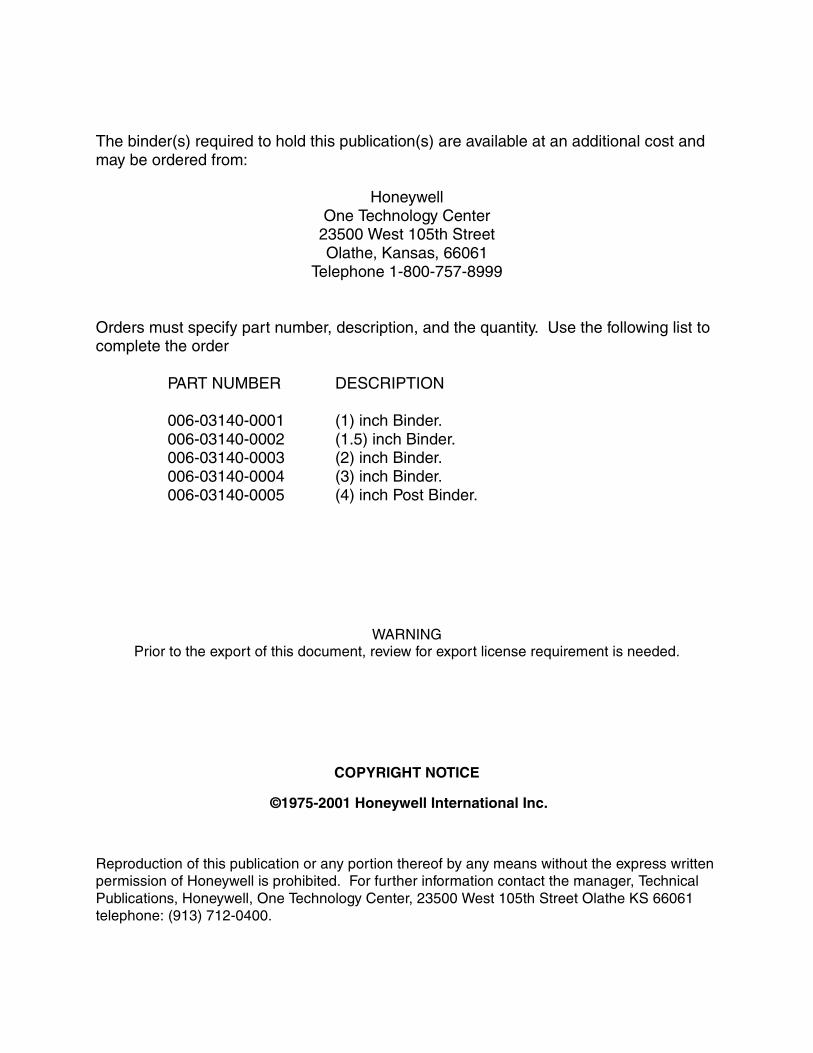
The binder(s) required to hold this publication(s) are available at an additional cost and may be ordered from:
HoneywellOne Technology Center
23500 West 105th StreetOlathe, Kansas, 66061
Telephone 1-800-757-8999
Orders must specify part number, description, and the quantity. Use the following list to complete the order
PART NUMBER DESCRIPTION
006-03140-0001 (1) inch Binder.006-03140-0002 (1.5) inch Binder.006-03140-0003 (2) inch Binder.006-03140-0004 (3) inch Binder.006-03140-0005 (4) inch Post Binder.
WARNINGPrior to the export of this document, review for export license requirement is needed.
COPYRIGHT NOTICE
©1975-2001 Honeywell International Inc.
Reproduction of this publication or any portion thereof by any means without the express written permission of Honeywell is prohibited. For further information contact the manager, Technical Publications, Honeywell, One Technology Center, 23500 West 105th Street Olathe KS 66061 telephone: (913) 712-0400.
BENDIX/KING KA 51B
Rev 7, Aug/2001 15627M07.JA Page RH-1
REVISION HISTORY
KA 51B Maintenance Manual
Part Number: 006-15627-XXXX
For each revision, add, delete, or replace pages as indicated.
REVISION No. 7, August 2001
Revision 7 creates a new stand-alone manual for the KA 51B which was extracted from revision 6 of the KCS 55/55A maintenance manual, (P/N 006-05111-0006). Any revisions to the KA 51B, beginning with revision 7, will not be a part of the KCS 55/55A manual.
ITEM ACTION
All pages Full Reprint, new manual

BENDIX/KING KA 51B
Page RH-2 15627M07.JA Rev 7, Aug/2001
THIS PAGE IS RESERVED
BENDIX/KING KA 51B
Rev 7, Aug/2001 15627M07.JA Page i
TABLE OF CONTENTS
SECTION IVTHEORY OF OPERATION
PARAGRAPH PAGE
4.1 General 4-1
4.2 Slave Meter Description 4-1
4.3 Auto-Manual Slave Switch Operation 4-1
4.4 Flux Valve Compensation Circuit 4-2
SECTION VMAINTENANCE
PARAGRAPH PAGE
5.1 General Information 5-1
5.2 Test and Alignment 5-1
5.2.1 Conditions of Testing 5-1
5.2.2 Signal Test Sources and Test Equipment 5-1
5.2.3 Minimum Performance 5-1
5.3 Overhaul 5-5
5.3.1 Visual Inspection 5-5
5.3.2 Cleaning 5-6
5.3.3 Repair 5-11
5.3.4 Disassembly/Assembly Procedures 5-15
5.4 Troubleshooting 5-15
SECTION VIILLUSTRATED PARTS LIST
PARAGRAPH PAGE
6.1 General 6-1
6.2 Revision Service 6-1
6.3 List of Abbreviations 6-1
6.4 Sample Parts List 6-3
6.5 KA 51B Final Assembly 6-5
6.6 KA 51B Compensator Assembly 6-13
BENDIX/KING KA 51B
Page ii 15627M07.JA Rev 7, Aug/2001
SECTION VIILLUSTRATED PARTS LIST (cont.)
PARAGRAPH PAGE
6.7 KA 51B Compensator Board 6-19
6.8 KA 51B Board 6-27
LIST OF ILLUSTRATIONS
FIGURE PAGE
4-1 Slave Meter System Diagram 4-1
4-2 KA 51B Compensator System Diagram 4-2
4-3 KA 51B 800Hz Generator Circuit 4-2
4-4 E/W Compensation Diagram 4-3
4-5 N/S Compensation Schematic 4-3
5-1 Waveform 5-2
5-2 Waveform 5-3
5-3 Waveform 5-3
5-4 KA 51B Test Circuit 5-4
5-5 KA 51B Troubleshooting Flow Chart 5-16
6-1 Sample Parts List 6-3
6-2 KA 51B Final Assembly 6-9
6-3 KA 51B Compensator Assembly 6-15
6-4 KA 51B Compensator Board 6-21
6-5 KA 51B Compensator Board Schematic 6-23
6-6 KA 51B Board 6-29
BENDIX/KING KA 51B
Rev 7, Aug/2001 15627M07.JA Page 4-1
SECTION IVTHEORY OF OPERATION
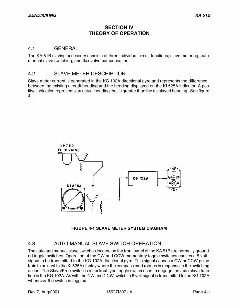
4.1 GENERALThe KA 51B slaving accessory consists of three individual circuit functions; slave metering, auto-manual slave switching, and flux valve compensation.
4.2 SLAVE METER DESCRIPTIONSlave meter current is generated in the KG 102A directional gyro and represents the difference between the existing aircraft heading and the heading displayed on the KI 525A indicator. A pos-itive indication represents an actual heading that is greater than the displayed heading. See figure 4-1.
FIGURE 4-1 SLAVE METER SYSTEM DIAGRAM
4.3 AUTO-MANUAL SLAVE SWITCH OPERATIONThe auto and manual slave switches located on the front panel of the KA 51B are normally ground-ed toggle switches. Operation of the CW and CCW momentary toggle switches causes a 5 volt signal to be transmitted to the KG 102A directional gyro. This signal causes a CW or CCW pulse train to be sent to the KI 525A display where the compass card rotates in response to the switching action. The Slave/Free switch is a Lockout type toggle switch used to engage the auto slave func-tion in the KG 102A. As with the CW and CCW switch, a 5 volt signal is transmitted to the KG 102A whenever the switch is toggled.
BENDIX/KING KA 51B
Page 4-2 15627M07.JA Rev 7, Aug/2001
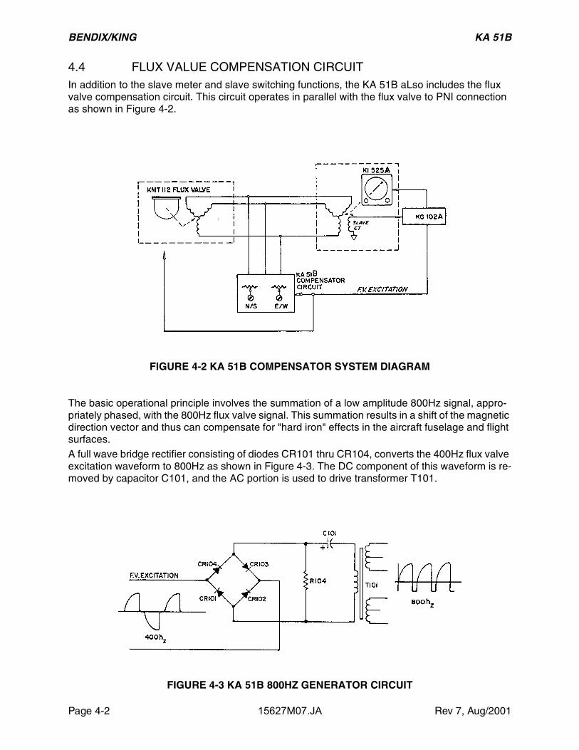
4.4 FLUX VALUE COMPENSATION CIRCUITIn addition to the slave meter and slave switching functions, the KA 51B aLso includes the flux valve compensation circuit. This circuit operates in parallel with the flux valve to PNI connection as shown in Figure 4-2.
FIGURE 4-2 KA 51B COMPENSATOR SYSTEM DIAGRAM
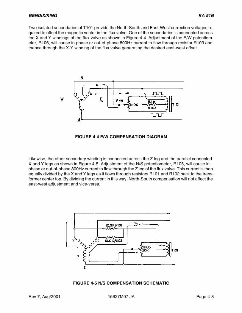
The basic operational principle involves the summation of a low amplitude 800Hz signal, appro-priately phased, with the 800Hz flux valve signal. This summation results in a shift of the magnetic direction vector and thus can compensate for "hard iron" effects in the aircraft fuselage and flight surfaces.A full wave bridge rectifier consisting of diodes CR101 thru CR104, converts the 400Hz flux valve excitation waveform to 800Hz as shown in Figure 4-3. The DC component of this waveform is re-moved by capacitor C101, and the AC portion is used to drive transformer T101.
FIGURE 4-3 KA 51B 800HZ GENERATOR CIRCUIT
BENDIX/KING KA 51B
Rev 7, Aug/2001 15627M07.JA Page 4-3
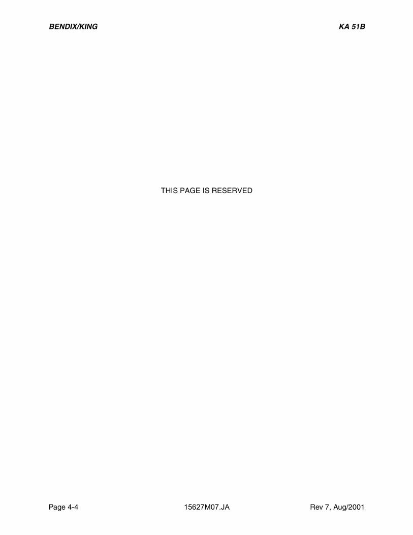
Two isolated secondaries of T101 provide the North-South and East-West correction voltages re-quired to offset the magnetic vector in the flux valve. One of the secondaries is connected across the X and Y windings of the flux valve as shown in Figure 4-4. Adjustment of the E/W potentiom-eter, R106, will cause in-phase or out-of-phase 800Hz current to flow through resistor R103 and thence through the X-Y winding of the flux valve generating the desired east-west offset.
FIGURE 4-4 E/W COMPENSATION DIAGRAM
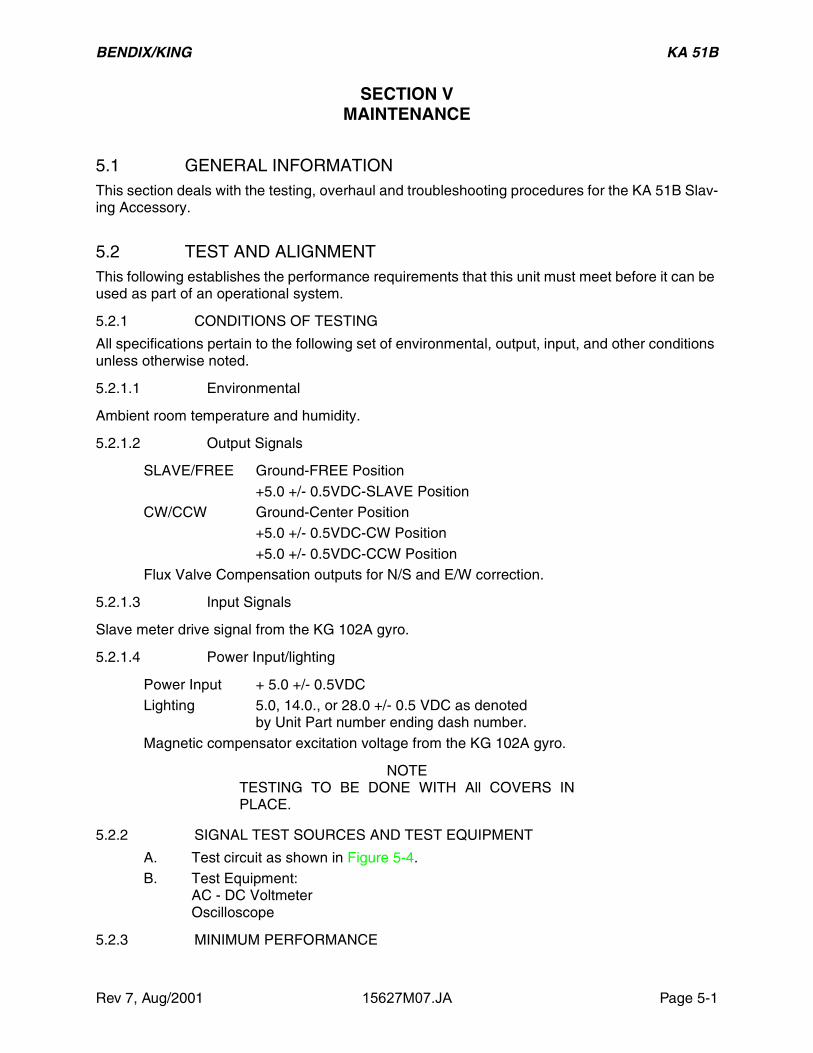
Likewise, the other secondary winding is connected across the Z leg and the parallel connected X and Y legs as shown in Figure 4-5. Adjustment of the N/S potentiometer, R105, will cause in-phase or out-of-phase 800Hz current to flow through the Z leg of the flux valve. This current is then equally divided by the X and Y legs as it flows through resistors R101 and R102 back to the trans-former center top. By dividing the current in this way, North-South compensation will not affect the east-west adjustment and vice-versa.
FIGURE 4-5 N/S COMPENSATION SCHEMATIC
BENDIX/KING KA 51B
Page 4-4 15627M07.JA Rev 7, Aug/2001
THIS PAGE IS RESERVED
BENDIX/KING KA 51B
Rev 7, Aug/2001 15627M07.JA Page 5-1
SECTION VMAINTENANCE
5.1 GENERAL INFORMATIONThis section deals with the testing, overhaul and troubleshooting procedures for the KA 51B Slav-ing Accessory.
5.2 TEST AND ALIGNMENTThis following establishes the performance requirements that this unit must meet before it can be used as part of an operational system.
5.2.1 CONDITIONS OF TESTING
All specifications pertain to the following set of environmental, output, input, and other conditions unless otherwise noted.
5.2.1.1 Environmental
Ambient room temperature and humidity.
5.2.1.2 Output Signals
SLAVE/FREE Ground-FREE Position+5.0 +/- 0.5VDC-SLAVE Position
CW/CCW Ground-Center Position+5.0 +/- 0.5VDC-CW Position+5.0 +/- 0.5VDC-CCW Position
Flux Valve Compensation outputs for N/S and E/W correction.
5.2.1.3 Input Signals
Slave meter drive signal from the KG 102A gyro.
5.2.1.4 Power Input/lighting
Power Input + 5.0 +/- 0.5VDCLighting 5.0, 14.0., or 28.0 +/- 0.5 VDC as denoted
by Unit Part number ending dash number.Magnetic compensator excitation voltage from the KG 102A gyro.
NOTETESTING TO BE DONE WITH All COVERS INPLACE.
5.2.2 SIGNAL TEST SOURCES AND TEST EQUIPMENT
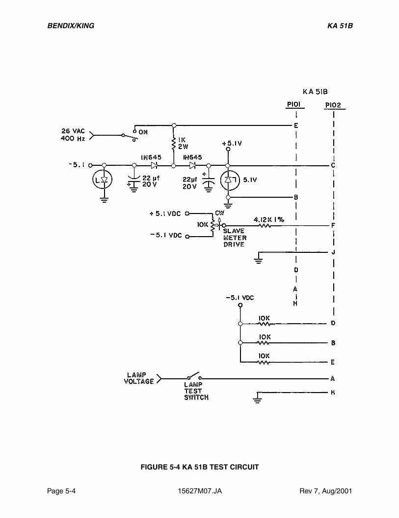
A. Test circuit as shown in Figure 5-4.B. Test Equipment:
AC - DC VoltmeterOscilloscope
5.2.3 MINIMUM PERFORMANCE
BENDIX/KING KA 51B
Page 5-2 15627M07.JA Rev 7, Aug/2001
A. Connect the unit to the test circuit shown in Figure 5-4. Switch the 26VAC on and record the following voltages:1. Pin C of P102 +5.1 +/-1VDC2. Pin D of P102 0.0 +/-0.05VDC3. Pin B of P102 0.0 +/-0.05VDC4. Pin E of P102 0.0 +/-0.05VDC5. Pin E of P101 26 +/-VAC
B. Switch the SLAVE/FREE switch to the SLAVE position.Pin D of P102 +5.1 +/-1VDCPin B of P102 0.0 +/-0.05VDCPin E of P102 0.0 +/-0.05VDC
C. Switch the SLAVE/FREE switch to the FREE position. Hold the CW/CCW switch in the CCW position.
Pin D of P102 0.0 +/-0.05VDCPin 8 of P102 +5.1 +/-1VDCPin E of P102 0.0 +/-0.05VDCRelease the CCW slave toggle. The toggle shall return to the center position.
D. Hold the CW/CCW switch in the CW positionPin D of P102 0.0 +/-0.05VDCPin B of P102 0.0 +/-0.05VDCPin E of P102 +5.1 +/-1VDC
Release the CW slave toggle. The toggle shall return to the center position.E. Adjust the slave meter pot to position the slave meter needle over the neg full scale
mark.Pin F of P102 -0.70 + 0.15VDCRepeat for the positive full scale mark.Pin F of P102 +0.70 + 0.15VDC
F. Adjust the slave meter pot for 0.0 +/-0.05VDC at Pin F of P102. The slave meter shall be within 1/2 needles width of center scale.
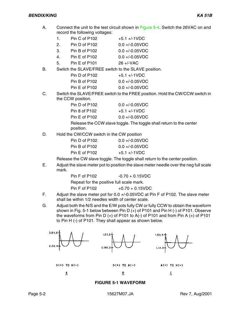
G. Adjust both the N/S and the E/W pots fully CW or fully CCW to obtain the waveform shown in Fig. 5-1 below between Pin D (+) of P101 and Pin H (-) of P101. Observe the waveforms from Pin D (+) of P101 to A(-) of P101 and from Pin A (+) of P101 to Pin H (-) of P101. They shall appear as shown below.
FIGURE 5-1 WAVEFORM
BENDIX/KING KA 51B
Rev 7, Aug/2001 15627M07.JA Page 5-3
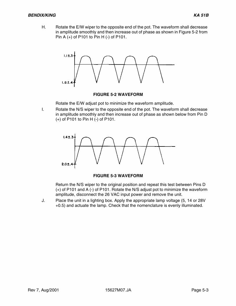
H. Rotate the E/W wiper to the opposite end of the pot. The waveform shall decrease in amplitude smoothly and then increase out of phase as shown in Figure 5-2 from Pin A (+) of P101 to Pin H (-) of P101.
FIGURE 5-2 WAVEFORM
Rotate the E/W adjust pot to minimize the waveform amplitude.I. Rotate the N/S wiper to the opposite end of the pot. The waveform shall decrease
in amplitude smoothly and then increase out of phase as shown below from Pin D (+) of P101 to Pin H (-) of P101.
FIGURE 5-3 WAVEFORM
Return the N/S wiper to the original position and repeat this test between Pins D (+) of P101 and A (-) of P101. Rotate the N/S adjust pot to minimize the waveform amplitude, disconnect the 26 VAC input power and remove the unit.
J. Place the unit in a lighting box. Apply the appropriate lamp voltage (5, 14 or 28V +0.5) and actuate the lamp. Check that the nomenclature is evenly illuminated.
BENDIX/KING KA 51B
Page 5-4 15627M07.JA Rev 7, Aug/2001
FIGURE 5-4 KA 51B TEST CIRCUIT
BENDIX/KING KA 51B
Rev 7, Aug/2001 15627M07.JA Page 5-5
5.3 OVERHAUL
5.3.1 VISUAL INSPECTION
This section contains instructions and information to assist in determining, by visual inspection, the condition of the units major assemblies and subassemblies. These inspection procedures will assist in finding defects resulting from wear, physical damage, deterioration, or other causes. To aid inspection, detailed procedures are arranged in alphabetical order.
A. Capacitors, FixedInspect capacitors for case damage, body damage, and cracked, broken, or charred insulation. Check for loose, broken, or corroded terminal studs, lugs, or leads. Inspect for loose, broken, or improperly soldered connections. On chip caps, be especially alert for hairline cracks in the body and broken terminations.
B. Capacitors, VariableInspect trimmers for chipped and cracked bodies, damaged dielectrics, and dam-aged contacts.
C. ChassisInspect the chassis for loose or missing mounting hardware, deformation, dents, damaged fasteners, or damaged connectors. In addition, check for corrosion or damage to the finish that should be repaired.
D. Circuit BoardsInspect for loose, broken, or corroded terminal connections; insufficient solder or improper bonding; fungus, mold, or other deposits; and damage such as cracks, burns, or charred traces.
E. ConnectorsInspect the connector bodies for broken parts; check the insulation for cracks, and check the contacts for damage, misalignment, corrosion, or bad plating. Check for broken, loose, or poorly soldered connections to terminals of the connectors. In-spect connector hoods and cable clamps for crimped wires.
F. Covers and ShieldsInspect covers and shields for punctures, deep dents, and badly worn surfaces. Al-so, check for damaged fastener devices, corrosion and damage to finish.
G. Flex CircuitsInspect flex circuits for punctures, and badly worn surfaces. Check for broken trac-es, especially near the solder contact points.
H. Front PanelCheck that name, serial, and any plates or stickers are secure and hardware is tight. Check that the handle is functional, securely fastened, and handle casting is not damaged or bent.
I. FuseInspect for blown fuse and check for loose solder joints.
J. InsulatorsInspect insulators for evidence of damage, such as broken or chipped edges, burned areas, and presence of foreign matter.
K. JacksInspect all jacks for corrosion, rust, deformations, loose or broken parts, cracked insulation, bad contacts, or other irregularities.
BENDIX/KING KA 51B
Page 5-6 15627M07.JA Rev 7, Aug/2001
L. PotentiometersInspect all potentiometers for evidence of damage or loose terminals, cracked in-sulation or other irregularities.
M. Resistors, FixedInspect the fixed resistors for cracked, broken, blistered, or charred bodies and loose, broken, or improperly soldered connections. On chip resistors, be especially alert for hairline cracks in the body and broken terminations.
N. RF CoilsInspect all RF coils for broken leads, loose mountings, and loose, improperly sol-dered, or broken terminal connections. Check for crushed, scratched, cut or charred windings. Inspect the windings, leads, terminals and connections for cor-rosion or physical damage. Check for physical damage to forms and tuning slug adjustment screws.
O. Terminal Connections Soldered(1) Inspect for cold-soldered or resin joints. These joints present a po-
rous or dull, rough appearance. Check for strength of bond using the points of a tool.
(2) Examine the terminals for excess solder, protrusions from the joint, pieces adhering to adjacent insulation, and particles lodged be-tween joints, conductors, or other components.
(3) Inspect for insufficient solder and unsoldered strands of wire pro-truding from the conductor at the terminal. Check for insulation that is stripped back too far from the terminal.
(4) Inspect for corrosion at the terminal.P. Transformers
(1) Inspect for signs of excessive heating, physical damage to the case, cracked or broken insulation, and other abnormal conditions.
(2) Inspect for corroded, poorly soldered, or loose connecting leads or terminals.
Q. Wiring/Coaxial CableInspect wiring in chassis for breaks in insulation, conductor breaks, cut or broken lacing and improper dress in relation to adjacent wiring or chassis.
5.3.2 CLEANING
A. GeneralThis section contains information to aid in the cleaning of the component parts and subassemblies of the unit.
WARNING:GOGGLES ARE TO BE WORN WHEN USINGPRESSURIZED AIR TO BLOW DUST ANDDIRT FROM EQUIPMENT. ALL PERSONNELSHOULD BE WARNED AWAY FROM THE IM-MEDIATE AREA.
BENDIX/KING KA 51B
Rev 7, Aug/2001 15627M07.JA Page 5-7
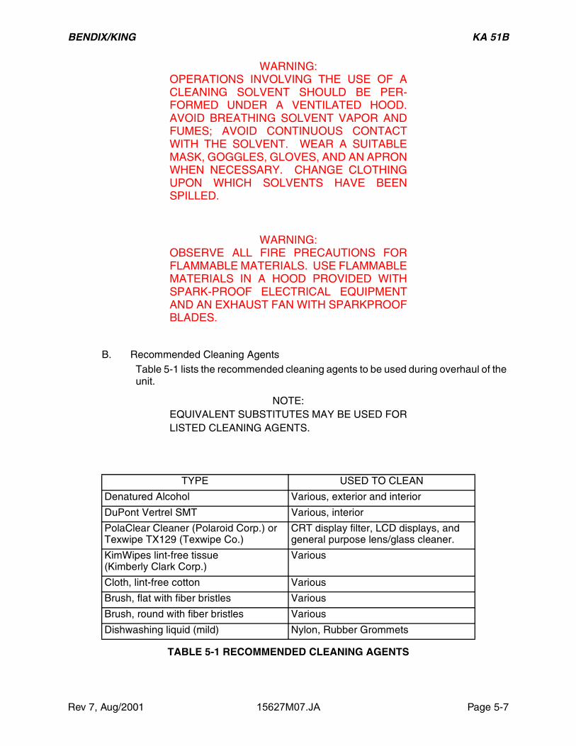
WARNING:OPERATIONS INVOLVING THE USE OF ACLEANING SOLVENT SHOULD BE PER-FORMED UNDER A VENTILATED HOOD.AVOID BREATHING SOLVENT VAPOR ANDFUMES; AVOID CONTINUOUS CONTACTWITH THE SOLVENT. WEAR A SUITABLEMASK, GOGGLES, GLOVES, AND AN APRONWHEN NECESSARY. CHANGE CLOTHINGUPON WHICH SOLVENTS HAVE BEENSPILLED.
WARNING:OBSERVE ALL FIRE PRECAUTIONS FORFLAMMABLE MATERIALS. USE FLAMMABLEMATERIALS IN A HOOD PROVIDED WITHSPARK-PROOF ELECTRICAL EQUIPMENTAND AN EXHAUST FAN WITH SPARKPROOFBLADES.
B. Recommended Cleaning AgentsTable 5-1 lists the recommended cleaning agents to be used during overhaul of the unit.
NOTE:EQUIVALENT SUBSTITUTES MAY BE USED FORLISTED CLEANING AGENTS.
TABLE 5-1 RECOMMENDED CLEANING AGENTS
TYPE USED TO CLEAN
Denatured Alcohol Various, exterior and interior
DuPont Vertrel SMT Various, interior
PolaClear Cleaner (Polaroid Corp.) or Texwipe TX129 (Texwipe Co.)
CRT display filter, LCD displays, and general purpose lens/glass cleaner.
KimWipes lint-free tissue(Kimberly Clark Corp.)
Various
Cloth, lint-free cotton Various
Brush, flat with fiber bristles Various
Brush, round with fiber bristles Various
Dishwashing liquid (mild) Nylon, Rubber Grommets
BENDIX/KING KA 51B
Page 5-8 15627M07.JA Rev 7, Aug/2001
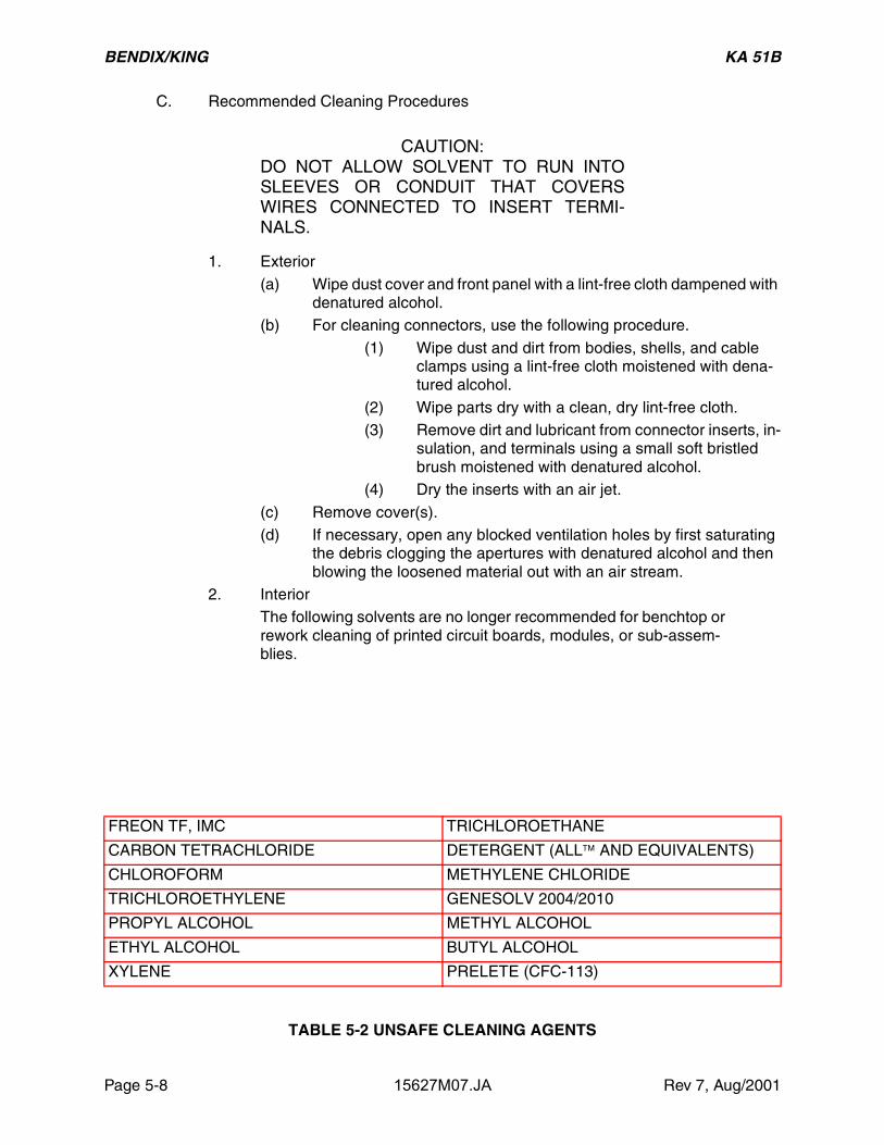
C. Recommended Cleaning Procedures
CAUTION:DO NOT ALLOW SOLVENT TO RUN INTOSLEEVES OR CONDUIT THAT COVERSWIRES CONNECTED TO INSERT TERMI-NALS.
1. Exterior(a) Wipe dust cover and front panel with a lint-free cloth dampened with
denatured alcohol.(b) For cleaning connectors, use the following procedure.
(1) Wipe dust and dirt from bodies, shells, and cable clamps using a lint-free cloth moistened with dena-tured alcohol.
(2) Wipe parts dry with a clean, dry lint-free cloth.(3) Remove dirt and lubricant from connector inserts, in-
sulation, and terminals using a small soft bristled brush moistened with denatured alcohol.
(4) Dry the inserts with an air jet.(c) Remove cover(s).(d) If necessary, open any blocked ventilation holes by first saturating
the debris clogging the apertures with denatured alcohol and then blowing the loosened material out with an air stream.
2. InteriorThe following solvents are no longer recommended for benchtop or rework cleaning of printed circuit boards, modules, or sub-assem-blies.
TABLE 5-2 UNSAFE CLEANING AGENTS
FREON TF, IMC TRICHLOROETHANE
CARBON TETRACHLORIDE DETERGENT (ALL AND EQUIVALENTS)
CHLOROFORM METHYLENE CHLORIDE
TRICHLOROETHYLENE GENESOLV 2004/2010
PROPYL ALCOHOL METHYL ALCOHOL
ETHYL ALCOHOL BUTYL ALCOHOL
XYLENE PRELETE (CFC-113)
BENDIX/KING KA 51B
Rev 7, Aug/2001 15627M07.JA Page 5-9
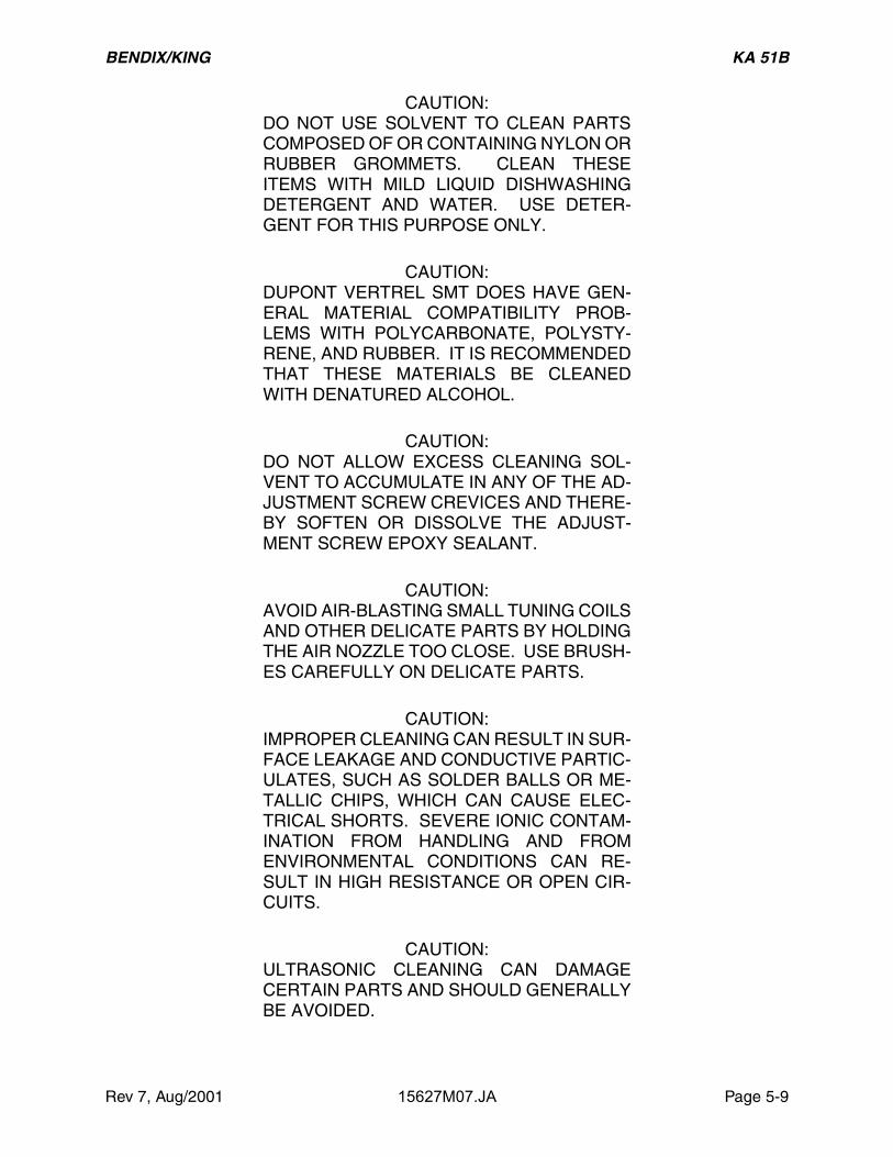
CAUTION:DO NOT USE SOLVENT TO CLEAN PARTSCOMPOSED OF OR CONTAINING NYLON ORRUBBER GROMMETS. CLEAN THESEITEMS WITH MILD LIQUID DISHWASHINGDETERGENT AND WATER. USE DETER-GENT FOR THIS PURPOSE ONLY.
CAUTION:DUPONT VERTREL SMT DOES HAVE GEN-ERAL MATERIAL COMPATIBILITY PROB-LEMS WITH POLYCARBONATE, POLYSTY-RENE, AND RUBBER. IT IS RECOMMENDEDTHAT THESE MATERIALS BE CLEANEDWITH DENATURED ALCOHOL.
CAUTION:DO NOT ALLOW EXCESS CLEANING SOL-VENT TO ACCUMULATE IN ANY OF THE AD-JUSTMENT SCREW CREVICES AND THERE-BY SOFTEN OR DISSOLVE THE ADJUST-MENT SCREW EPOXY SEALANT.
CAUTION:AVOID AIR-BLASTING SMALL TUNING COILSAND OTHER DELICATE PARTS BY HOLDINGTHE AIR NOZZLE TOO CLOSE. USE BRUSH-ES CAREFULLY ON DELICATE PARTS.
CAUTION:IMPROPER CLEANING CAN RESULT IN SUR-FACE LEAKAGE AND CONDUCTIVE PARTIC-ULATES, SUCH AS SOLDER BALLS OR ME-TALLIC CHIPS, WHICH CAN CAUSE ELEC-TRICAL SHORTS. SEVERE IONIC CONTAM-INATION FROM HANDLING AND FROMENVIRONMENTAL CONDITIONS CAN RE-SULT IN HIGH RESISTANCE OR OPEN CIR-CUITS.
CAUTION:ULTRASONIC CLEANING CAN DAMAGECERTAIN PARTS AND SHOULD GENERALLYBE AVOIDED.
BENDIX/KING KA 51B
Page 5-10 15627M07.JA Rev 7, Aug/2001
NOTE:Solvents may be physically applied in several waysincluding agitation, spraying, brushing, and vapordegreasing. The cleaning solvents and methodsused shall have no deleterious effect on the parts,connections, and materials being used. If sensitivecomponents are being used, spray is recommended.Uniformity of solvent spray flow should be maxi-mized and wait-time between soldering and cleaningshould be minimized.
NOTE:Clean each module subassembly. Then remove anyforeign matter from the casting.
Remove each module subassembly. Then remove any foreign mat-ter from the casting.(a) Casting covers and shields should be cleaned as follows:
(1) Remove surface grease with a lint-free cloth.(2) Blow dust from surfaces, holes, and recesses using
an air stream.(3) If necessary, use a solvent, and scrub until clean,
working over all surfaces and into all holes and re-cesses with a suitable non-metallic brush.
(4) Position the part to dry so the solvent is not trapped in holes or recesses. Use an air stream to blow out any trapped solvent.
(5) When thoroughly clean, touch up any minor damage to the finish.
(b) Assemblies containing resistors, capacitors, rf coils, inductors, transformers, and other wired parts should be cleaned as follows:
(1) Remove dust and dirt from all surfaces, including all parts and wiring, using soft-bristled brushes in con-junction with air stream.
(2) Any dirt that cannot be removed in this way should be removed with a brush (not synthetic) saturated with an approved solvent, such as mentioned above. Use of a clean, dry air stream (25 to 28 psi) is recom-mended to remove any excess solvent.
(3) Remove flux residue, metallic chips, and/or solder balls with an approved solvent.
(c) Wired chassic devices containing terminal boards, resistor and ca-pacitor assemblies, rf coils, switches, sockets, inductors, transform-ers, and other wired parts should be cleaned as follows:
BENDIX/KING KA 51B
Rev 7, Aug/2001 15627M07.JA Page 5-11
NOTE:When necessary to disturb the dress of wires andcables, note the positions before disturbing and re-store them to proper dress after cleaning.
(1) Blow dust from surfaces, holes, and recesses using an air jet.
(2) Finish cleaning chassis by wiping finished surfaces with a lint-free cloth moistened with solvent.
(3) Dry with a clean, dry, lint-free cloth.(4) When thoroughly clean, touch-up any minor damage
to the finish.(5) Protect the chassis from dust, moisture, and damage
pending inspection.(d) Ceramic and plastic parts should be cleaned as follows:
(1) Blow dust from surfaces, holes, and recesses using an air jet.
(2) Finish cleaning chassis by wiping finished surfaces with a lint-free cloth moistened with solvents.
(3) Dry with a clean, dry, lint-free cloth.
5.3.3 REPAIR
A. GeneralThis section contains information required to perform limited repairs on the unit. The repair or replacement of damaged parts in airborne electronic equipment usu-ally involves standard service techniques. In most cases, examination of drawings and equipment reveals several approaches to perform a repair. However, certain repairs demand following an exact repair sequence to ensure proper operation of the equipment. After correcting a malfunction in any section of the unit, it is recom-mended that a repetition of the functional test of the unit be performed.
B. Repair Precautions1. Ensure that all ESDS and MOS handling precautions are followed.2. Perform repairs and replace components with power disconnected
from equipment.3. Use a conductive table top for repairs and connect table to ground
conductors of 60Hz and 400Hz power lines.4. Replace connectors, coaxial cables, shield conductors, and twisted
pairs only with identical items.5. Reference “component side” of a printed circuit board in this manual
means the side on which components are located; “solder side” re-fers to the other side. The standard references are as follows: near-side is the component side; farside is the solder side; on surface mount boards with components on both sides, the nearside is the side that has the J#### and P#### connector numbers.
6. When repairing circuits, carefully observe lead dress and compo-nent orientation. Keep leads as short as possible and observe cor-rect repair techniques.
BENDIX/KING KA 51B
Page 5-12 15627M07.JA Rev 7, Aug/2001
7. There are certain soldering considerations with surface mount com-ponents. The soldering iron tip should not touch the ceramic com-ponent body. The iron should be applied only to the termination-sol-der filet.
8. Observe cable routing throughout instrument assembly, prior to dis-assembly, to enable a proper reinstallation of cabling during reas-sembly procedures.
CAUTIONTHIS EQUIPMENT CONTAINS ELECTRO-STATIC DISCHARGE SENSITIVE (ESDS) DE-VICES. EQUIPMENT MODULES AND ESDSDEVICES MUST BE HANDLED IN ACCOR-DANCE WITH SPECIAL ESDS HANDLINGPROCEDURES.
C. Electrostatic Sensitive Devices (ESDS) Protection1. Always discharge static before handling devices by touching some-
thing that is grounded.2. Use a wrist strap grounded through a 1MΩ resistor.3. Do not slide anything on the bench. Pick it up and set it down in-
stead.4. Keep all parts in protective cartons until ready to insert into the
board.5. Never touch the device leads or the circuit paths during assembly.6. Use a grounded tip, low wattage soldering station.7. Keep the humidity in the work environment as high as feasibly pos-
sible.8. Use grounded mats on the work station unless table tops are made
of approved antistatic material.9. Do not use synthetic carpet on the floor of the shop. If a shop is car-
peted, ensure that a grounded mat is placed at each workstation.10. Keep common plastics out of the work area.
D. MOS Device ProtectionMOS (Metal Oxide Semiconductor) devices are used in this equipment. While the attributes of MOS type devices are many, characteristics make them susceptible to damage by electrostatic or high voltage charges. Therefore, special precautions must be taken during repair procedures to prevent damaging the device. The fol-lowing precautions are recommended for MOS circuits, and are especially impor-tant in low humidity or dry conditions.1. Store and transport all MOS devices in conductive material so that
all exposed leads are shorted together. Do not insert MOS devices into conventional plastic “snow” or plastic trays used for storing and transporting standard semiconductor devices.

BENDIX/KING KA 51B
Rev 7, Aug/2001 15627M07.JA Page 5-13
2. Ground working surfaces on workbench to protect the MOS devic-es.
3. Wear cotton gloves or a conductive wrist strap in series with a 200KΩ resistor connected to ground.
4. Do not wear nylon clothing while handling MOS devices.5. Do not insert or remove MOS devices with power applied. Check all
power supplies to be used for testing MOS devices. and be sure that there are no voltage transients present.
6. When straightening MOS leads, provide ground straps for the appa-ratus for the device.
7. Ground the soldering iron when soldering a device.8. When possible, handle all MOS devices by package or case, and
not by leads. Prior to touching the device, touch an electrical ground to displace any accumulated static charge. The package and substrate may be electrically common. If so, an electrical dis-charge to the case would cause the same damage as touching the leads.
9. Clamping or holding fixtures used during repair should be ground-ed, as should the circuit board, during repair.
10. Devices should be inserted into the printed circuit boards such that leads on the back side do not contact any material other than the printed circuit board (in particular, do not use any plastic foam as a backing).
11. Devices should be soldered as soon as possible after assembly. All soldering irons must be grounded.
12. Boards should not be handled in the area around devices, but rather by board edges.
13. Assembled boards must not be placed in conventional, home-type, plastic bags. Paper bags or antistatic bags should be used.
14. Before removing devices from conductive portion of the device car-rier, make certain conductive portion of carrier is brought in contact with well grounded table top.
E. PC Board, Two-Lead Component Removal (Resistors, Capacitors, Diodes, etc.)1. Heat one lead from component side of board until solder flows, and
lift one lead from board; repeat for other lead and remove compo-nent (note orientation).
2. Melt solder in each hole, and using a desoldering tool, remove sol-der from each hole.
3. Dress and form leads of replacement component; insert leads into correct holes.
4. Insert replacement component observing correct orientation.
F. PC Board, Multi-Lead Component Removal (IC’s, etc.)1. Remove component by clipping each lead along both sides. Clip off
leads as close to component as possible. Discard component.2. Heat hole from solder side and remove clipped lead from each hole.
BENDIX/KING KA 51B
Page 5-14 15627M07.JA Rev 7, Aug/2001
3. Melt solder in each hole, and using a desoldering tool, remove sol-der from each hole.
4. Insert replacement component observing correct orientation.5. Solder component in place from farside of board. Avoid solder runs.
No solder is required on contacts where no traces exist.
G. Replacement of Power Transistors1. Unsolder leads and remove attaching hardware. Remove transistor
and hard-coat insulator.2. Apply Thermal Joint Compound Type 120 (Wakefield Engineering,
Inc.) to the mounting surface of the replacement transistor.3. Reinstall the transistor insulator and the power transistor using
hardware removed in step (1).4. After installing the replacement transistor, but before making any
electrical connections, measure the resistance between the case of the transistor and the chassis, to ensure that the insulation is effec-tive. The resistance measured should be greater than 10MΩ.
5. Reconnect leads to transistor and solder in place.
H. Replacement of Printed Circuit Board Protective Coating
WARNINGCONFORMAL COATING CONTAINS TOXICVAPORS! USE ONLY WITH ADEQUATE VEN-TILATION.
1. Clean repaired area of printed circuit board per instructions in the Cleaning section of this manual.
2. Apply Conformal Coating, Humiseal #1B-31 HYSOL PC20-35M-01 (Humiseal Division, Columbia Chase Corp., 24-60 Brooklyn Queens Expressway West, Woodside, N.Y., 11377) P/N 016-01040-0000.
3. Shake container well before using.4. Spray or brush surfaces with smooth, even strikes. If spraying, hold
nozzle 10-15 inches from work surface.5. Cure time is ten minutes at room temperature.
I. Programmable Read Only Memory (PROM) ReplacementThe read only memory packages are specially programmed devices to provide specific logic outputs required for operation in the unit. The manufacturer’s part (type) number is for the un-programmed device, and cannot be used. The Honey-well part number must be used to obtain the correctly programmed device. Refer to the “Illustrated Parts List” (IPL).
BENDIX/KING KA 51B
Rev 7, Aug/2001 15627M07.JA Page 5-15
5.3.3.1 REPLACEMENT OF COMPONENTS
This section describes the procedure, along with any special techniques, for replacing damaged or defective components.
A. ConnectorsWhen replacing a connector, refer to the appropriate PC board assembly drawing, and follow the notes, to ensure correct mounting and mating of each connector.
B. CrystalThe use of any crystal, other than a Honeywell crystal, is considered an unautho-rized modification.
C. DiodesDiodes used are silicon and germanium. Use long-nose pliers as a heat sink, under normal soldering conditions. Note the diode polarity before removal.
D. Integrated CircuitsRefer to the applicable reference for removal and replacement instructions.
E. Wiring/Coaxial CableWhen repairing a wire that has broken from its terminal, remove all old solder, and pieces of wire from the terminal, re-strip the wire to the necessary length, and resol-der the wire to the terminal. Replace a damaged wire or coaxial cable with one of the same type, size and length.
5.3.4 DISASSEMBLY/ASSEMBLY PROCEDURES
The following instructions included the procedures that are necessary to remove and disassemble the subassemblies of the KA 51B.It is assumed that the unit has been tested in accordance with Section 5.2 to locate the source of the malfunction. The unit should be disassembled only to the point where the malfunction can be corrected by repair, cleaning, or adjustment. Do not disassemble any parts or wiring unnecessarily as repeated tear downs can be detrimental to the life of the unit.The KA 51B is comprised of a final assembly and one major subassembly. Disassembly instruc-tions are provided to separate the subassembly from the basic unit. Reassembly can be accom-plished by reversing the disassembly procedures. Refer to the subassembly drawings in Section VI during disassembly or assembly.
5.3.4.1 P.C. BOARD REMOVAL
A. Remove the Compensator Assembly from the front section by removing the two screws at the pigtail end.
B. Remove the two screws that hold the plate to the compensator housing.C. Remove the tie-wrap that secured the pigtail to the housing.D. Slide the printed circuit board out of the housing.E. When in this state of disassembly, the components of the printed circuit board are
readily accessible.
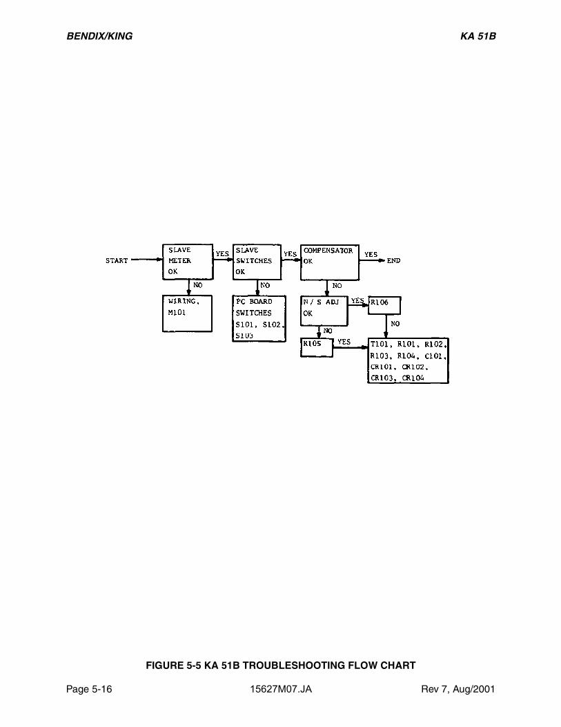
5.4 TROUBLESHOOTINGRefer to the troubleshooting flow chart, figure 5-5.
BENDIX/KING KA 51B
Page 5-16 15627M07.JA Rev 7, Aug/2001
FIGURE 5-5 KA 51B TROUBLESHOOTING FLOW CHART
BENDIX/KING KA 51B
Rev 7, Aug/2001 15627M07.JA Page 6-1
ILLUSTRATED PARTS LIST
6.1 General
The Illustrated Parts List (IPL) is a complete list of assemblies and parts required for the unit. The IPL also provides for the proper identification of replacement parts. Individual parts lists within this IPL are arranged in numerical sequence starting with the top assembly and continuing with the sub-assemblies. All me-chanical parts will be separated from the electrical parts used on the sub-assembly. Each parts list is followed by a component location drawing.
Parts identified in this IPL by Honeywell part number meet design specifications for this equipment and are the recommended replacement parts. Warranty informa-tion concerning Honeywell replacement parts is contained in Service Memo #1, P/N 600-08001-00XX.
Some part numbers may not be currently available. Consult the current Honeywell catalog or contact a Honeywell representative for equipment availability.
6.2 Revision Service
The manual will be revised as necessary to reflect current information.
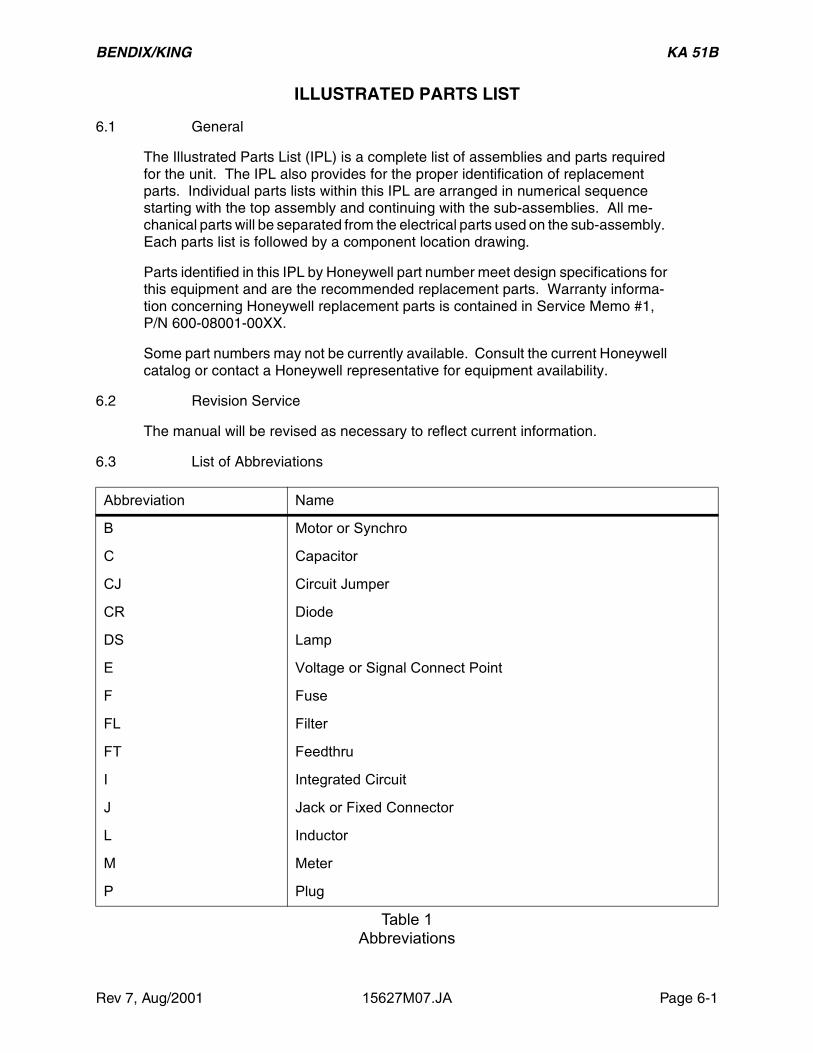
6.3 List of Abbreviations
Abbreviation Name
B Motor or Synchro
C Capacitor
CJ Circuit Jumper
CR Diode
DS Lamp
E Voltage or Signal Connect Point
F Fuse
FL Filter
FT Feedthru
I Integrated Circuit
J Jack or Fixed Connector
L Inductor
M Meter
P Plug
Table 1 Abbreviations
BENDIX/KING KA 51B
Page 6-2 15627M07.JA Rev 7, Aug/2001
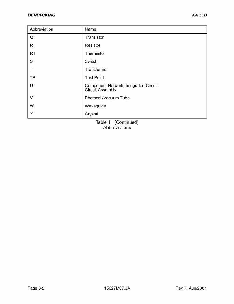
Q Transistor
R Resistor
RT Thermistor
S Switch
T Transformer
TP Test Point
U Component Network, Integrated Circuit,Circuit Assembly
V Photocell/Vacuum Tube
W Waveguide
Y Crystal
Abbreviation Name
Table 1 (Continued) Abbreviations
BENDIX/KING KA 51B
Rev 7, Aug/2001 15627M07.JA Page 6-3
6.4 Sample Parts List
The above is only a sample. The actual format and style may vary slightly. A ‘Find Number’ column, when shown, references selected items on the BOM’s accompa-nying Assembly Drawing. This information does not apply to every BOM. There-fore, a lack of information in this column, or a lack of this column, should not be interpreted as an omission.
Figure 6-1 Sample Parts List

BENDIX/KING KA 51B
Page 6-4 15627M07.JA Rev 7, Aug/2001
THIS PAGE IS RESERVED
BENDIX/KING KA 51B
Rev 7, Aug/2001 15627M07.JA Page 6-5
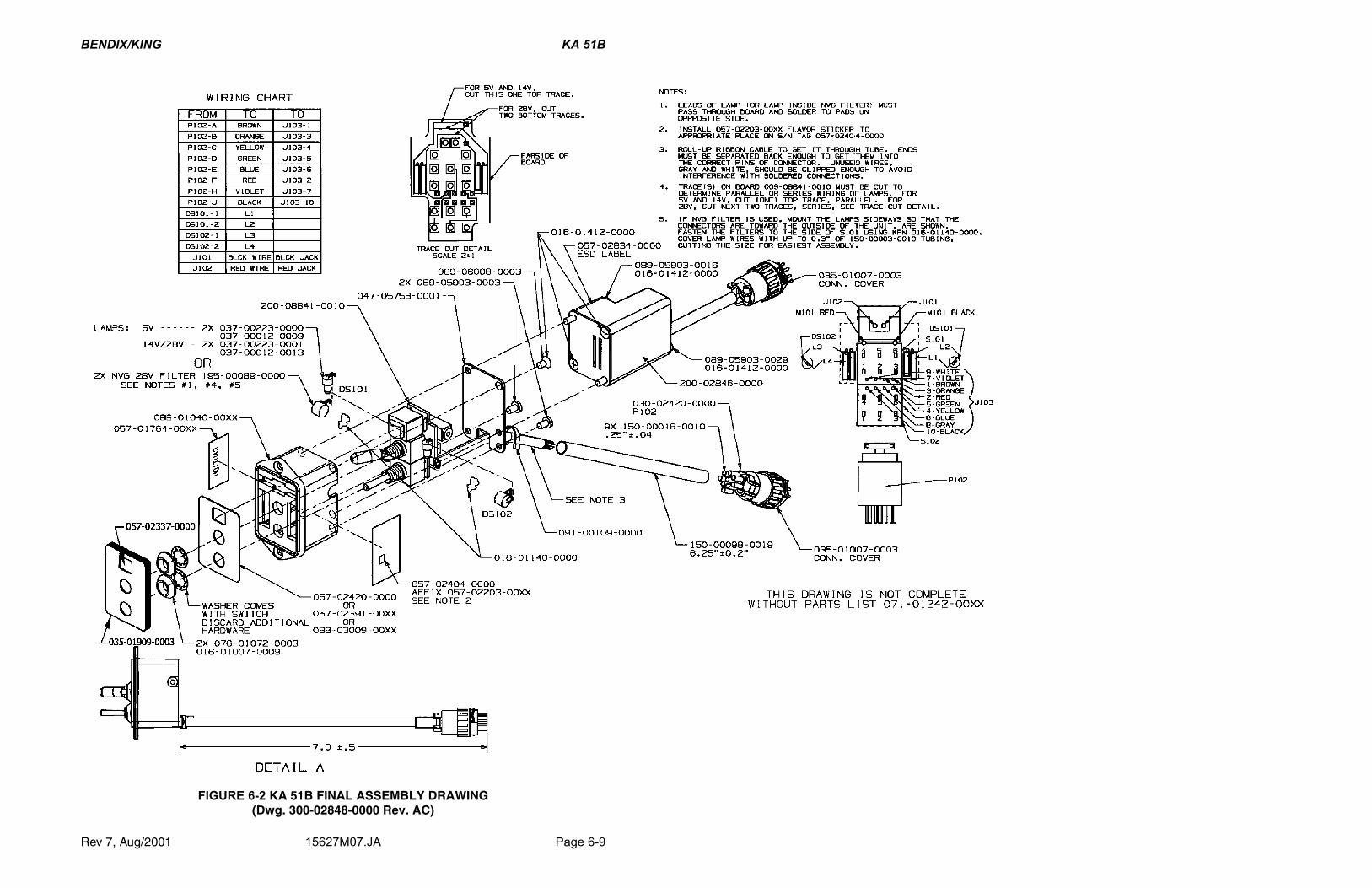
6.5 KA 51B FINAL ASSEMBLY
071-01242-0000 Rev. 4071-01242-0001 Rev. 5071-01242-0002 Rev. 5071-01242-0003 Rev. 3071-01242-0004 Rev. 3071-01242-0005 Rev. 4071-01242-0006 Rev. 5071-01242-0007 Rev. 6071-01242-0008 Rev. 6071-01242-0009 Rev. 6071-01242-0010 Rev. 6071-01242-0011 Rev. 7071-01242-0012 Rev. AB071-01242-0013 Rev. 4071-01242-0014 Rev. 4071-01242-0099 Rev. AB
-----------------------------------------------------------------------------SYMBOL PART NUMBER FIND NO DESCRIPTION UM 0000 0001 0002-----------------------------------------------------------------------------DS101 037-00223-0001 LAMP BLUE FILTERED EA 1.00 1.00 1.00DS102 037-00223-0001 LAMP BLUE FILTERED EA 1.00 1.00 1.00REF1 300-02848-0000 FINAL ASSEMBLY KA RF .00 .00 .00 057-01764-0001 WRN TAG 14V LGT EA 1.00 . . 057-01764-0002 WRN TAG 28V LGT EA . 1.00 1.00 057-02203-0000 FLAVOR STCKR EA 1.00 . . 057-02203-0001 FLAVOR STCKR EA . 1.00 . 057-02203-0002 FLAVOR STCKR EA . . 1.00 057-02391-0000 TAPE INSERT BLACK EA 1.00 1.00 . 057-02391-0001 TAPE INSERT GRAY EA . . 1.00 071-01242-0099 SLAV ACCES CMN B/M EA 1.00 1.00 1.00 088-01040-0003 FACEPLATE W/F EA 1.00 1.00 . 088-01040-0004 FACEPLATE W/F EA . . 1.00
BENDIX/KING KA 51B
Page 6-6 15627M07.JA Rev 7, Aug/2001
-----------------------------------------------------------------------------SYMBOL PART NUMBER FIND NO DESCRIPTION UM 0003 0004 0005-----------------------------------------------------------------------------DS101 037-00012-0009 LAMP MIN T-1 5V EA 1.00 . . DS101 037-00012-0013 LAMP MIN T-1 28V EA . 1.00 . DS101 037-00223-0001 LAMP BLUE FILTERED EA . . 1.00DS102 037-00012-0009 LAMP MIN T-1 5V EA 1.00 . . DS102 037-00012-0013 LAMP MIN T-1 28V EA . 1.00 . DS102 037-00223-0001 LAMP BLUE FILTERED EA . . 1.00REF1 300-02848-0000 FINAL ASSEMBLY KA RF .00 .00 .00 057-01764-0000 WRN TAG 5V LGT EA 1.00 . . 057-01764-0001 WRN TAG 14V LGT EA . . 1.00 057-01764-0002 WRN TAG 28V LGT EA . 1.00 . 057-02203-0003 FLAVOR STCKR EA 1.00 . . 057-02203-0004 FLAVOR STCKR EA . 1.00 . 057-02203-0005 FLAVOR STCKR EA . . 1.00 057-02391-0000 TAPE INSERT BLACK EA 1.00 1.00 . 057-02420-0000 TAPE INSERT EA . . 1.00 071-01242-0099 SLAV ACCES CMN B/M EA 1.00 1.00 1.00 088-00084-0000 FILTER LAMP RED EA 2.00 2.00 . 088-01040-0003 FACEPLATE W/F EA 1.00 1.00 1.00
-----------------------------------------------------------------------------SYMBOL PART NUMBER FIND NO DESCRIPTION UM 0006 0007 0008-----------------------------------------------------------------------------DS101 037-00223-0000 LAMP BLUE FILTERED EA . 1.00 1.00DS101 037-00223-0001 LAMP BLUE FILTERED EA 1.00 . . DS102 037-00223-0000 LAMP BLUE FILTERED EA . 1.00 1.00DS102 037-00223-0001 LAMP BLUE FILTERED EA 1.00 . . REF1 300-02848-0000 FINAL ASSEMBLY KA RF .00 .00 .00 057-01764-0000 WRN TAG 5V LGT EA . 1.00 1.00 057-01764-0002 WRN TAG 28V LGT EA 1.00 . . 057-02203-0006 FLAVOR STCKR EA 1.00 . . 057-02203-0007 FLAVOR STCKR EA . 1.00 . 057-02203-0008 FLAVOR STCKR EA . . 1.00 057-02391-0001 TAPE INSERT GRAY EA . . 1.00 057-02420-0000 TAPE INSERT EA 1.00 . . 057-02420-0001 TAPE INSERT GRY EA . 1.00 . 071-01242-0099 SLAV ACCES CMN B/M EA 1.00 1.00 1.00 088-01040-0003 FACEPLATE W/F EA 1.00 . . 088-01040-0004 FACEPLATE W/F EA . 1.00 1.00
BENDIX/KING KA 51B
Rev 7, Aug/2001 15627M07.JA Page 6-7
-----------------------------------------------------------------------------SYMBOL PART NUMBER FIND NO DESCRIPTION UM 0009 0010 0011-----------------------------------------------------------------------------DS101 037-00223-0000 LAMP BLUE FILTERED EA . 1.00 1.00DS101 037-00223-0001 LAMP BLUE FILTERED EA 1.00 . . DS102 037-00223-0000 LAMP BLUE FILTERED EA . 1.00 1.00DS102 037-00223-0001 LAMP BLUE FILTERED EA 1.00 . . REF1 300-02848-0000 FINAL ASSEMBLY KA RF .00 .00 .00 057-01764-0000 WRN TAG 5V LGT EA . 1.00 1.00 057-01764-0002 WRN TAG 28V LGT EA 1.00 . . 057-02203-0009 FLAVOR STCKR EA 1.00 . . 057-02203-0011 FLAVOR STICKER EA . . 1.00 057-02391-0000 TAPE INSERT BLACK EA . 1.00 . 057-02420-0000 TAPE INSERT EA . . 1.00 057-02420-0001 TAPE INSERT GRY EA 1.00 . . 071-01242-0099 SLAV ACCES CMN B/M EA 1.00 1.00 1.00 088-01040-0003 FACEPLATE W/F EA . 1.00 1.00 088-01040-0004 FACEPLATE W/F EA 1.00 . .
-----------------------------------------------------------------------------SYMBOL PART NUMBER FIND NO DESCRIPTION UM 0012 0013 0014-----------------------------------------------------------------------------DS101 037-00223-0000 LAMP BLUE FILTERED EA . 1.00 1.00DS101 195-00089-0000 NVG FILTERED LAMP EA 1.00 . . DS102 037-00223-0000 LAMP BLUE FILTERED EA . 1.00 1.00DS102 195-00089-0000 NVG FILTERED LAMP EA 1.00 . . REF1 300-02848-0000 FINAL ASSEMBLY KA RF .00 .00 .00 016-01140-0000 SUPERBONDER 415 AR 1.00 . . 057-01764-0000 WRN TAG 5V LGT EA . 1.00 1.00 057-01764-0002 WRN TAG 28V LGT EA 1.00 . . 057-02203-0012 FLAVOR STCKR EA 1.00 . . 057-02203-0013 FLAVOR STCKR EA . 1.00 . 057-02203-0014 FLAVOR STCKR EA . . 1.00 057-02420-0000 TAPE INSERT EA 1.00 . . 057-02834-0000 ESD TAG EA 1.00 . . 071-01242-0099 SLAV ACCES CMN B/M EA 1.00 1.00 1.00 088-01040-0003 FACEPLATE W/F EA 1.00 . . 088-01040-0004 FACEPLATE W/F EA . 1.00 1.00 088-03009-0001 FACE PLATE EA . 1.00 . 088-03009-0002 FACE PLATE EA . . 1.00 150-00003-0010 TUBING TFLN 24AWG AR 1.00 . .
BENDIX/KING KA 51B
Page 6-8 15627M07.JA Rev 7, Aug/2001
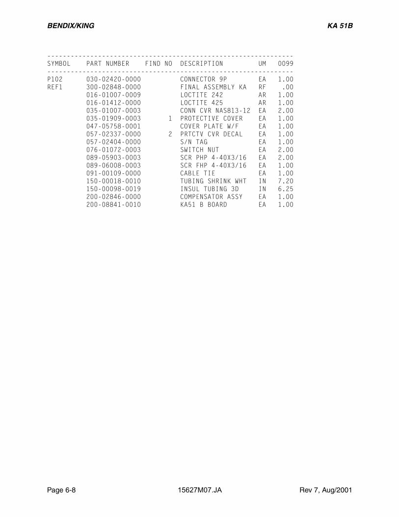
---------------------------------------------------------------SYMBOL PART NUMBER FIND NO DESCRIPTION UM 0099---------------------------------------------------------------P102 030-02420-0000 CONNECTOR 9P EA 1.00REF1 300-02848-0000 FINAL ASSEMBLY KA RF .00 016-01007-0009 LOCTITE 242 AR 1.00 016-01412-0000 LOCTITE 425 AR 1.00 035-01007-0003 CONN CVR NAS813-12 EA 2.00 035-01909-0003 1 PROTECTIVE COVER EA 1.00 047-05758-0001 COVER PLATE W/F EA 1.00 057-02337-0000 2 PRTCTV CVR DECAL EA 1.00 057-02404-0000 S/N TAG EA 1.00 076-01072-0003 SWITCH NUT EA 2.00 089-05903-0003 SCR PHP 4-40X3/16 EA 2.00 089-06008-0003 SCR FHP 4-40X3/16 EA 1.00 091-00109-0000 CABLE TIE EA 1.00 150-00018-0010 TUBING SHRINK WHT IN 7.20 150-00098-0019 INSUL TUBING 3D IN 6.25 200-02846-0000 COMPENSATOR ASSY EA 1.00 200-08841-0010 KA51 B BOARD EA 1.00
BENDIX/KING KA 51B
Rev 7, Aug/2001 15627M07.JA Page 6-9
FIGURE 6-2 KA 51B FINAL ASSEMBLY DRAWING(Dwg. 300-02848-0000 Rev. AC)
BENDIX/KING KA 51B
Rev 7, Aug/2001 15627M07.JA Page 6-11
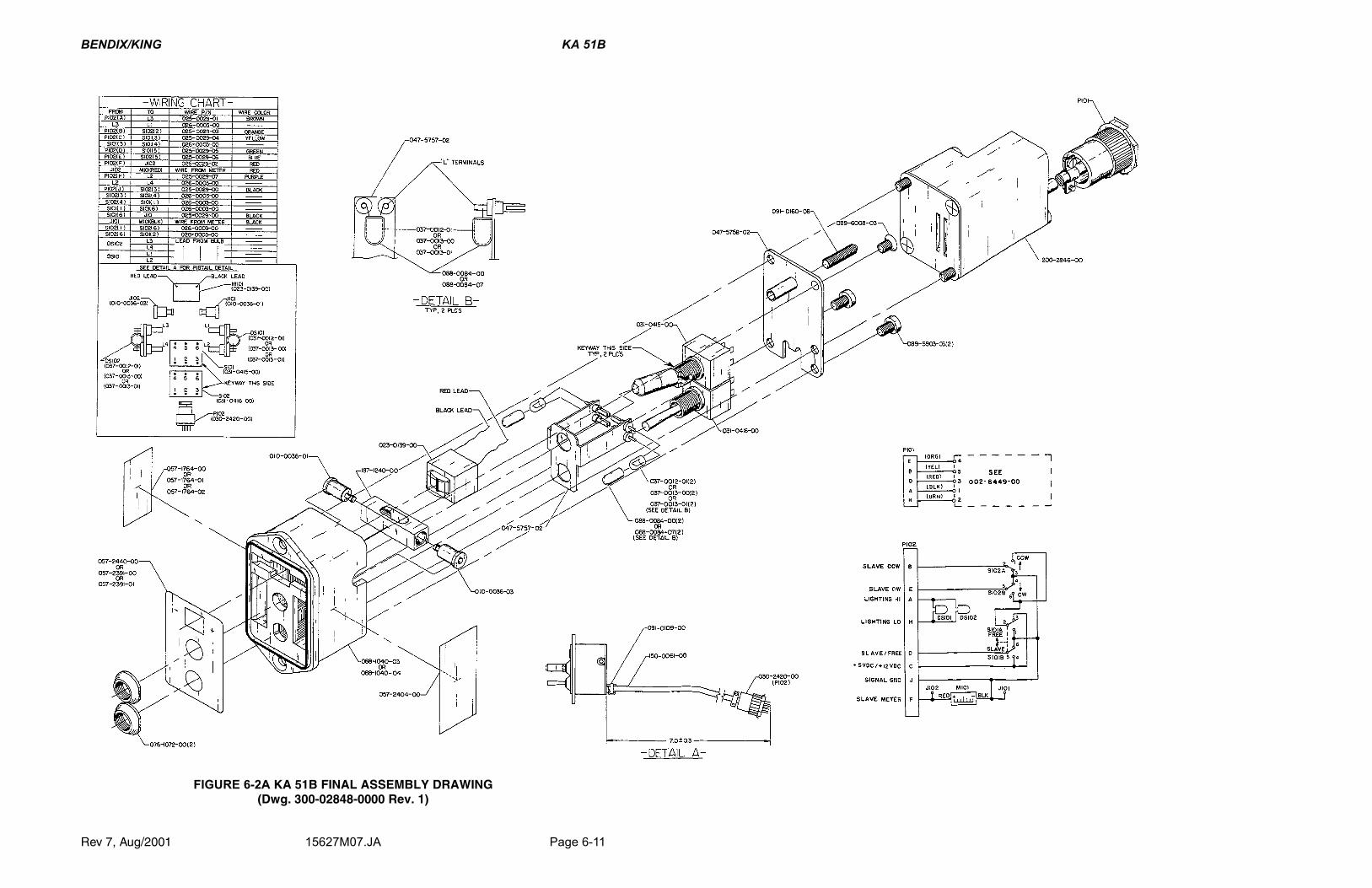
FIGURE 6-2A KA 51B FINAL ASSEMBLY DRAWING(Dwg. 300-02848-0000 Rev. 1)
BENDIX/KING KA 51B
Rev 7, Aug/2001 15627M07.JA Page 6-13
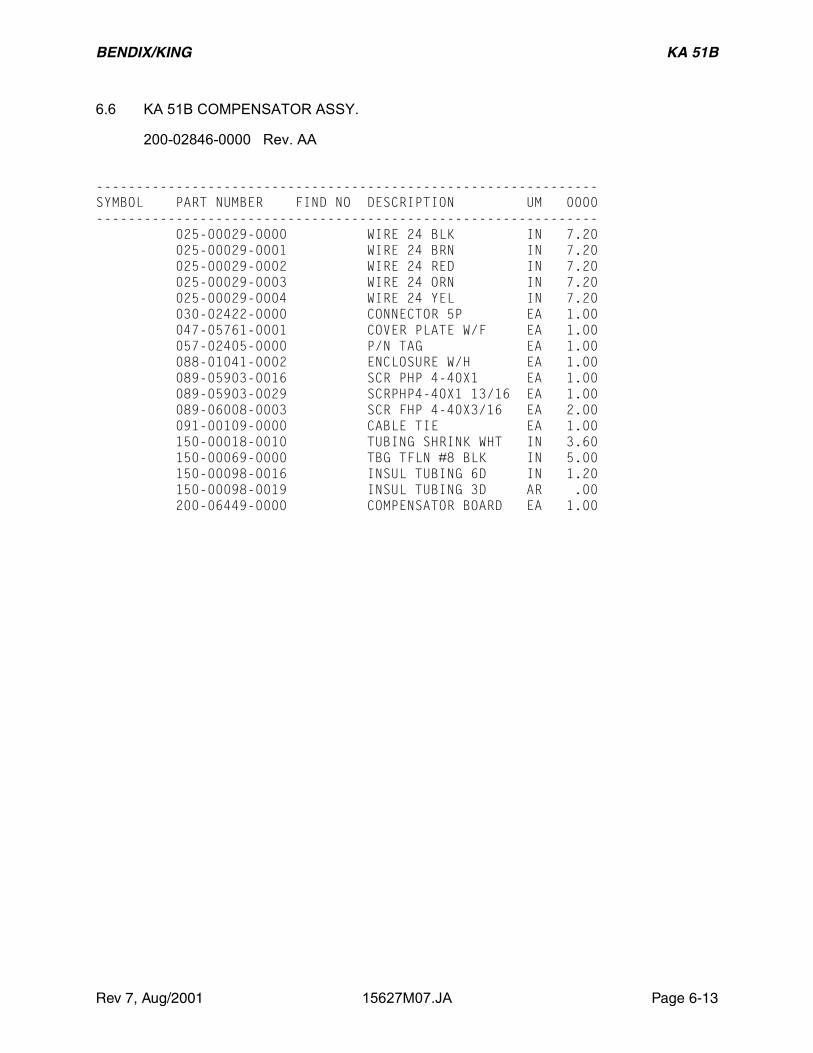
6.6 KA 51B COMPENSATOR ASSY.
200-02846-0000 Rev. AA
---------------------------------------------------------------SYMBOL PART NUMBER FIND NO DESCRIPTION UM 0000--------------------------------------------------------------- 025-00029-0000 WIRE 24 BLK IN 7.20 025-00029-0001 WIRE 24 BRN IN 7.20 025-00029-0002 WIRE 24 RED IN 7.20 025-00029-0003 WIRE 24 ORN IN 7.20 025-00029-0004 WIRE 24 YEL IN 7.20 030-02422-0000 CONNECTOR 5P EA 1.00 047-05761-0001 COVER PLATE W/F EA 1.00 057-02405-0000 P/N TAG EA 1.00 088-01041-0002 ENCLOSURE W/H EA 1.00 089-05903-0016 SCR PHP 4-40X1 EA 1.00 089-05903-0029 SCRPHP4-40X1 13/16 EA 1.00 089-06008-0003 SCR FHP 4-40X3/16 EA 2.00 091-00109-0000 CABLE TIE EA 1.00 150-00018-0010 TUBING SHRINK WHT IN 3.60 150-00069-0000 TBG TFLN #8 BLK IN 5.00 150-00098-0016 INSUL TUBING 6D IN 1.20 150-00098-0019 INSUL TUBING 3D AR .00 200-06449-0000 COMPENSATOR BOARD EA 1.00

BENDIX/KING KA 51B
Page 6-14 15627M07.JA Rev 7, Aug/2001
THIS PAGE IS RESERVED
BENDIX/KING KA 51B
Rev 7, Aug/2001 15627M07.JA Page 6-15
FIGURE 6-3 KA 51B COMPENSATOR ASSEMBLY DRAWING(Dwg. 300-02846-0000 Rev. AA)
BENDIX/KING KA 51B
Rev 7, Aug/2001 15627M07.JA Page 6-17
FIGURE 6-3A KA 51B COMPENSATOR ASSEMBLY DRAWING(Dwg. 300-02846-0000 Rev. 0)
BENDIX/KING KA 51B
Rev 7, Aug/2001 15627M07.JA Page 6-19
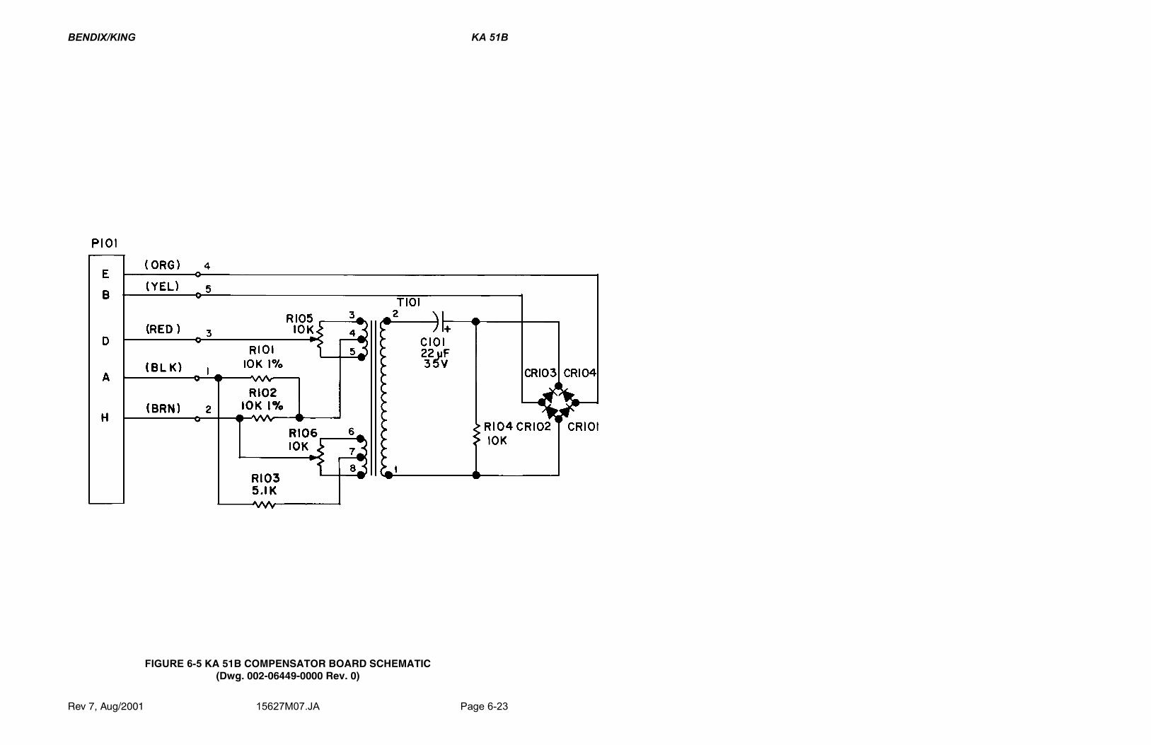
6.7 KA 51B COMPENSATOR BD
200-06449-0000 Rev. AA
---------------------------------------------------------------SYMBOL PART NUMBER FIND NO DESCRIPTION UM 0000---------------------------------------------------------------C101 096-01082-0030 CAP TN 22UF 35V EA 1.00CR101 007-06029-0000 DIO S 1N457A EA 1.00CR102 007-06029-0000 DIO S 1N457A EA 1.00CR103 007-06029-0000 DIO S 1N457A EA 1.00CR104 007-06029-0000 DIO S 1N457A EA 1.00R101 136-01002-0072 RES PF 10K QW 1% EA 1.00R102 136-01002-0072 RES PF 10K QW 1% EA 1.00R103 131-00512-0023 RES CF 5.1K QW 5% EA 1.00R104 131-00103-0023 RES CF 10K QW 5% EA 1.00R105 133-00113-0018 RES VA 10K 20% A EA 1.00R106 133-00113-0018 RES VA 10K 20% A EA 1.00T101 019-05069-0000 XFMR EA 1.00 002-06449-0000 SCHEMATIC PC BD KA RF .00 009-06449-0000 PC BD COMPENSATOR EA 1.00 016-01040-0000 COATING TYPE AR AR .00 192-06449-0000 KA 51B COMPENSATOR RF .00 300-06449-0000 COMPENSATOR BD RF .00

BENDIX/KING KA 51B
Page 6-20 15627M07.JA Rev 7, Aug/2001
THIS PAGE IS RESERVED
BENDIX/KING KA 51B
Rev 7, Aug/2001 15627M07.JA Page 6-21
FIGURE 6-4 KA 51B COMPENSATOR BOARD DRAWING(Dwg. 300-06449-0000 Rev. 2)
BENDIX/KING KA 51B
Rev 7, Aug/2001 15627M07.JA Page 6-23
FIGURE 6-5 KA 51B COMPENSATOR BOARD SCHEMATIC(Dwg. 002-06449-0000 Rev. 0)
BENDIX/KING KA 51B
Rev 7, Aug/2001 15627M07.JA Page 6-25
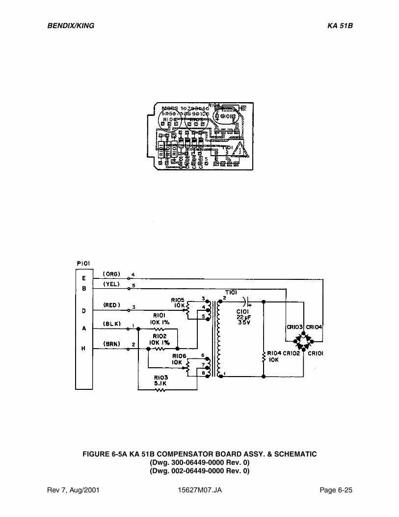
FIGURE 6-5A KA 51B COMPENSATOR BOARD ASSY. & SCHEMATIC(Dwg. 300-06449-0000 Rev. 0)(Dwg. 002-06449-0000 Rev. 0)
BENDIX/KING KA 51B
Page 6-26 15627M07.JA Rev 7, Aug/2001
THIS PAGE IS RESERVED
BENDIX/KING KA 51B
Rev 7, Aug/2001 15627M07.JA Page 6-27
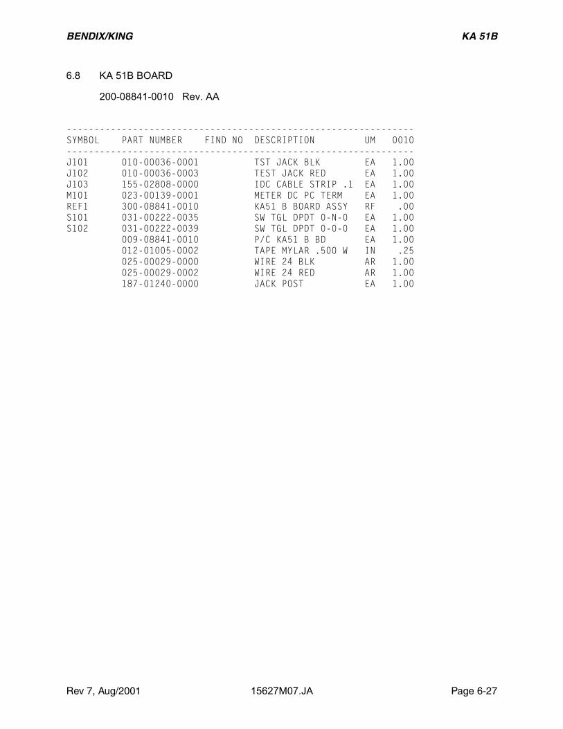
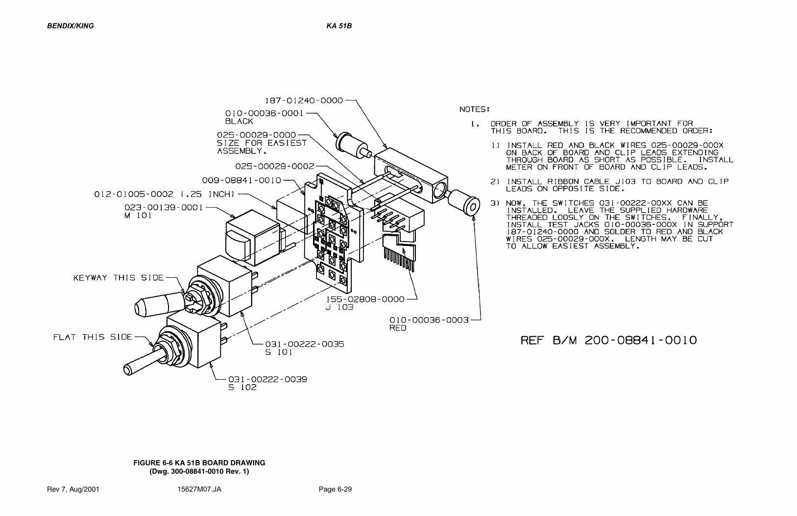
6.8 KA 51B BOARD
200-08841-0010 Rev. AA
---------------------------------------------------------------SYMBOL PART NUMBER FIND NO DESCRIPTION UM 0010---------------------------------------------------------------J101 010-00036-0001 TST JACK BLK EA 1.00J102 010-00036-0003 TEST JACK RED EA 1.00J103 155-02808-0000 IDC CABLE STRIP .1 EA 1.00M101 023-00139-0001 METER DC PC TERM EA 1.00REF1 300-08841-0010 KA51 B BOARD ASSY RF .00S101 031-00222-0035 SW TGL DPDT 0-N-0 EA 1.00S102 031-00222-0039 SW TGL DPDT 0-0-0 EA 1.00 009-08841-0010 P/C KA51 B BD EA 1.00 012-01005-0002 TAPE MYLAR .500 W IN .25 025-00029-0000 WIRE 24 BLK AR 1.00 025-00029-0002 WIRE 24 RED AR 1.00 187-01240-0000 JACK POST EA 1.00

BENDIX/KING KA 51B
Page 6-28 15627M07.JA Rev 7, Aug/2001
THIS PAGE IS RESERVED
BENDIX/KING KA 51B
Rev 7, Aug/2001 15627M07.JA Page 6-29
FIGURE 6-6 KA 51B BOARD DRAWING(Dwg. 300-08841-0010 Rev. 1)