Embed Size (px)
Citation preview

The Role of Defects in Functional Oxide Nanostructures
C. Sudakar†‡, Shubra Singh‡*, M.S. Ramachandra Rao‡*, G. Lawes†
†Department of Physics and Astronomy, Wayne State University, Detroit, MI 48201
‡Department of Physics, Indian Institute of Technology Madras, Chennai, India 600036
*Nano Functional Materials Technology Centre,
Indian Institute of Technology Madras, Chennai, India 600036
3.1 Introduction
The burgeoning interest in nanoscale metal oxides arises
from the recognition that the materials properties of these systems
depend strongly on morphology, allowing the development of new
or enhanced characteristics in geometrically restricted samples[1-3].
Finite size effects can produce significant changes in a number of in-
trinsic properties in systems having reduced length scales, including
the electronic band gap [4], the magnetic coercivity [5], and elastic
modulus [6], to name only a few of the characteristics that are
strongly sensitive to sample geometry. Simultaneously, the large
surface to volume ratio in nanomaterials, realized most dramatically
2
in nanoparticles, can also substantially affect the electronic [7], mag-
netic [8], optical [9], and elastic properties [10] of these systems.
Because of their relatively larger surface to volume ratio, the defect
concentration in metal oxide nanostructures is generally higher than
that found in bulk systems. These defects can have a profound ef-
fect on the physical properties of nanomaterials, so it is crucially im-
portant that they be fully considered when characterizing metal ox-
ide nanostructures. There are a number of thorough and accessible
reviews on defects in particular metal oxide systems, including ZnO
[11-14], TiO2 [15], and CuO [16] to name a few, along with more
comprehensive reports [17-18]. Rather than attempting to provide a
general overview of how defects modify the physical properties of
oxides, this particular report is more narrowly focused on briefly
presenting the entirely new properties and characteristics that can
emerge in metal oxide nano-systems due the presence of defects.
The chapter is structured as follows. We begin with a very
short review of the basic types of defects in metal oxides. Rather
than consider the multitude of possible defect structures, we sharply
limit our discussion to point defects. We will specifically focus on
3
oxygen defect vacancies (VO), metal ion vacancies (VM), and metal
interstitials (MI) since these are generally the most important and
widely studied intrinsic point defects in metal oxides [17-18]. The
bulk of the review will center on a discussion of the novel electrical,
optical, and magnetic properties that can arise in defect-rich metal
oxide systems. We will focus uniquely on the new physical behav-
iour that emerges due to the presence of defects and do not consider
in any depth the rather more widely studied problem of understand-
ing the role of defects in perturbing the existing properties of oxides.
We conclude with a short discussion of how these defect-induced
properties can be used to integrate new functionalities into metal ox-
ide nanostructures.
3.2 Defects in Metal Oxide Nanostructures
We broadly limit the scope of our discussion to point defects.
As the emphasis of this review is to consider defects in metal oxide
nanostructures, we further restrict ourselves to discussing only in-
trinsic defects, and only very briefly touch on dopant ions as point
defects. Within these constraints, a large number point defects can
4
be considered: oxygen vacancies (VO), metal vacancies (VM), oxy-
gen interstitials (OI), metal interstitials (MI), and anti-site defects
(MO or OM). In a large number of cases, the most stable and/or phys-
ically important defects are VO, VM, and MI [17-18] so we focus pri-
marily on these specific examples. The interactions among different
types of defects can play an important role in determining the physi-
cal properties of metal oxides. For example, because Sn is multiva-
lent, SnI point defects can readily form in SnO2, which, in turn, sup-
ports the formation of VO defects leading to n-type conductivity in
defect-rich SnO2 films [19]. Rather remarkably, the presence of
these defects alone in metal oxide nanomaterials is sufficient to pro-
duce new physical properties that are not simply perturbations of the
intrinsic characteristics of the defect-free parent oxide. Heuristi-
cally, these emergent properties can, in general, be understood to
arise from interactions among the point defects leading to collective
behaviour. Certain metal oxide nanostructures are typically able to
support a relatively high concentration of VO defects, with oxygen
non-stoichiometry reaching several percent near the surfaces of
nanoscale systems [20]. Because this relatively large defect concen-

5
tration, defect-defect correlations can affect the response of the sys-
tem [20-22].
3.2.1 Defect Structures in Metal Oxide Nanostructures
The concentration and distribution of defects determine a
number of properties of crystalline solids. In high quality crystals the
concentration of defects can be extremely small, leading to consider-
able experimental challenges in accurately determining this defect
concentration [23]. Crystalline solids contain a number of different
types of structural defects. Vacancies defects develop due to the ab-
sence of atoms in some lattice sites while interstitials arise from ex-
tra atoms occupying the space between the atoms in the lattice [18,
23]. Vacancies and interstitial atoms are point defects as these im-
perfections are limited to one unit cell and lead to deviations from
the crystalline order only in the immediate vicinity of the defect. In
addition to point defects, line and plane defects are very often found
in real crystal systems [18, 23]. Line defects are dislocations that are
characterized by displacements in the crystal structure along specific
directions [18, 23]. Examples of plane defects comprise stacking
6
faults, grain boundaries, and internal and external surfaces. A
schematic diagram of possible defects in crystalline metal oxide
nanostructures is shown in Fig. 1. These defects can profoundly
modify the physical properties of materials, including electrical, op-
tical, and magnetic response as we will discuss in the following.
Many metal oxides, including ZnO, TiO2, SnO2 and In2O3,
exhibit marked deviations from stoichiometry under specific anneal-
ing conditions including thermal annealing in vacuum [20, 24-25]
and under a finite metal vapor pressure [26-27]. A relatively small
degree of off-stoichiometry can be supported by the inclusion of
point defects, including VO and VM [23], and annealing can also pro-
mote the formation of intersitials and antisite defects. At small con-
centrations (0.1 to 1 at%) these point defects are typically assumed
to be randomly distributed throughout the lattice [23]. At higher de-
fect concentrations, a number of different types of defects can de-
velop, including multiple charge state defects and pairs or com-
plexes of defects [17-18, 23]. However, as we will discuss, many of
the properties of defect-rich metal oxides can be understood by con-
7
sidering segregated (though possibly interacting) point defects, so
we center our discussion to this class of structures.
3.2.2 Imaging Defects in Metal Oxide Nanostructures
At relatively small concentrations, the distribution of point
defects in oxides is determined solely by entropy considerations and
consists of randomly distributed defects [23]. At higher defect con-
centrations, enthalpy begins to affect the distribution, which leads to
the formation of new structures including defect clusters, superlat-
tice ordering and extended defects, shear planes, and discrete inter-
mediate phases [23]. Defect-rich TiO2 (see Fig. 2) is an example of
an oxide in which extended defects, including planar defects, are
formed by the accumulation and elimination of point defects, such as
oxygen vacancies in vacuum annealed samples, along specific crys-
tallographic planes [28]. These vacancies are eliminated by the for-
mation of shear planes in the crystal, which in turn produces a fault
in the cation sublattice [28]. Because of this interplay between point
defects and extended defect structures, in some metal oxide systems
8
it can be difficult to completely separate the two, as we illustrate in
the case of TiO2 and In2O3 in Fig. 2.
We first consider ideal, isolated point defects in ZnO as a
representative metal oxide system. In wurtzite ZnO the possible
point defects are: oxygen and zinc vacancies (VO, VZn), interstitials
(Oi, Zni), and antisite defects (OZn and ZnO). VO and Zni were most
generally considered to be the defects responsible for modifying the
electric and magnetic properties of the system [29-34]. However re-
cent work [11] suggests that these defects exhibit high formation en-
ergies under equilibrium conditions. Zn interstitials (Zni) are shallow
donors and fast diffusers with a low migration barrier, 0.57 eV, and
are therefore not stable at room temperature [11, 35]. VZn, which has
a low formation energy, is a deep acceptor, so is able to act as a
compensating center in n-type ZnO, and may be relevant for the
green luminescence observed in ZnO [11, 35]. Oi has a high energy
and acts as a deep acceptor at the octahedral site Oi-1(oct) in n-type
ZnO [11, 36]. The antisite defects (ZnO and OZn) have very high for-
mation energies and are unlikely under equilibrium conditions [11,
35-36].

9
The defect structure in metal oxide nanostructures can be im-
aged using high resolution transmission electron microscopy
(HRTEM). Comparing real-space images of air annealed and vac-
uum annealed In2O3 thin films clearly demonstrates the effects of
point defects on the nanostructure [20]. Fig. 2a shows a HRTEM
image of an air annealed In2O3 nanoparticle, showing a well-ordered
lattice with no obvious defects. Vacuum annealing this sample in-
troduces oxygen vacancies, as well as other point defects, as shown
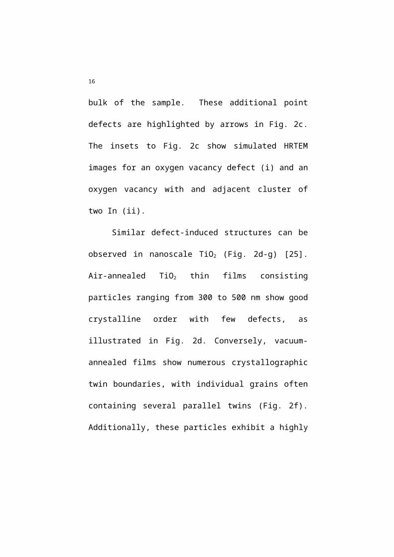
in Figs 2b and 2c. The agglomeration of point defects leads to a 2–3
nm thick surface disordered layer, as shown in Fig. 2b. Additional
point defects, both VO and InI, can be seen in the bulk of the sample.
These additional point defects are highlighted by arrows in Fig. 2c.
The insets to Fig. 2c show simulated HRTEM images for an oxygen
vacancy defect (i) and an oxygen vacancy with and adjacent cluster
of two In (ii).
Similar defect-induced structures can be observed in
nanoscale TiO2 (Fig. 2d-g) [25]. Air-annealed TiO2 thin films con-
sisting particles ranging from 300 to 500 nm show good crystalline
order with few defects, as illustrated in Fig. 2d. Conversely, vac-
10
uum-annealed films show numerous crystallographic twin bound-
aries, with individual grains often containing several parallel twins
(Fig. 2f). Additionally, these particles exhibit a highly disordered
surface phase of few nanometers thick [25]. These are common [28]
microstructural features in non-stoichiometric TiO2 and are inti-
mately related to the formation of shear structures discussed above.
The twinning produced in the rutile subcell structure is parallel to (0
1 1), which is the common twinning plane for TiO2 [28, 37-38]. This
twinning is not observed in TiO2 thin films formed from nanoparti-
cles [25]. However, a substantial non-stoichiometric disordered
phase develops at the surface of the nanoparticles (Fig. 2e), which
suggests that these planar defects may be more readily diffuse to the
surface under thermal annealing in films comprised of smaller parti-
cles.
3.2.3 Stability of Intrinsic Point Defects in Metal Oxide Nanos-
tructures
In order for these point defects to have any meaningful effect
on the properties of the metal oxide nanostructures in the context of
11
device applications, they should be stable under ambient conditions.
The determination of whether these defects are stable depends
strongly on the details of the specific metal oxide being considered.
In ZnO for example, the VO defects are believed to become stable in
presence of transition metal dopants such as Co [24]. In this particu-
lar study, oxygen defects were introduced in thin film ZnO samples
by annealing at high temperatures (600 oC) and low pressures (~10-6
torr). Raman spectral modes related to –Zn-O-Co- local disordered
vibrations in the stoichiometric (or defect-poor) Co:ZnO films disap-
pear after vacuum annealing as the oxygen vacant sites are localized
near Co site (–Zn-VO-Co-). In a number of systems, however, oxy-
gen vacancy defects may not be stable. Studies on oxygen deficient
TiO2 found that the concentration of VO defects decreases rapidly
under ambient conditions [25], although these defects can apparently
be stabilized by transition metal doping [32, 39-40]. Conversely, in
In2O3 nanostructured films, the oxygen vacancy defects are stable for
a timescale of years under the same conditions [41]. Because of this
sensitive dependence of the persistence of point defects on the spe-
cific compound being considered, it is important to properly charac-

12
terize the stability of these defects in a particular metal oxide when
determining the effects such defects may have on the physical prop-
erties of the material.
3.3 Electrical Response
Metal oxides exhibit a range of electrical transport properties,
from metallic to insulating to superconducting [37, 42-43]. The in-
troduction of point defects generically affects all types of electrical
transport, through mechanisms ranging from increased scattering in
metallic systems to the introduction of additional charge carriers in
insulators. We are particularly interested in exploring systems in
which the inclusion of point defects qualitatively changes the electri-
cal transport properties. We therefore limit our discussion to consid-
ering the onset of metallic or quasi-metallic conductivity induced by
point defects in systems where the undoped metal oxide is insulating
or semiconducting.
3.3.1 Point Defects and Charge Carriers
13
In general terms, point defects in metal oxide nanostructures
act like charge centers [44], which can lead to very high electrical
conductivities. Experimentally, a number of metal oxide systems
that are insulating when prepared as perfectly stoichiometric sam-
ples develop good electrical conductivity with the introduction of
point defects [14, 45]. In the simplest models, this increase in con-
ductivity requires shallow donors near the conduction band [46], or
acceptors near the valence band [47]. Many, though by no means
all, defect-rich oxide materials are found to exhibit n-type conduc-
tivity, pointing to an abundance of excess electrons associated with
the defects. VO sites, which normally act as electron donors, are a
possible point defect in all metal oxide systems and it is often be-
lieved that the conducting properties in these materials arise from
oxygen vacancy defects [48]. While we see that oxygen vacancy de-
fects do play a crucial role in mediating electrical conductivity in
many metal oxide materials, other types of point defects can also
have a significant effect on transport in defect-rich samples.
ZnO represents one of the most intensely investigated metal
oxide system [49-51] in the past decade. While oxygen vacancy de-

14
fects, possibly together with Zn interstitials, had been widely consid-
ered to be the origin of the n-type conductivity in this system [12,
48], recent studies suggest that other point defects may be more rele-
vant for determining the electrical transport properties [11]. These
investigations find that VO sites are deep donors, falling approxi-
mately 1 eV below the conduction band, and are thus unlikely to in-
troduce any significant of n-type charge carriers. The concentration
of Zn interstitials is found to have a high formation energy in n-type
materials, making ZnI defects unlikely as the source for increased
conductivity in defect-rich ZnO [11]. Upon considering all native
point defects in ZnO, the authors conclude that none of these is
likely to produce the observed n-type conductivity and instead pro-
pose that the charge carriers arise from the accidental inclusion of
substitutional hydrogen, HO, which can act as a shallow donor [52].
Along a similar line, experimental studies on the conductivity of
ZnO films prepared by pulsed laser deposition provide evidence that
nitrogen inclusions may play an important role in the development
of n-type conductivity in ZnO [46], with other work pointing to the
importance of hydrogen donors [53].
15
Indium oxide is another widely studied electronic material,
but there still remain a number of unanswered questions concerning
the fundamental transport properties in this system [54]. In2O3 can
exhibit a high degree of non-stoichiometry and shows extremely
good n-type dopability [55-58]. It has been suggested that In2O3 is an
anion-deficient n-type conductor, but that the small oxygen vacancy
defect population, corresponding to approximately 1% of the anions,
limits the electron concentration [59]. Experimentally, it is found
that oxygen deficient In2O3 is highly compensated, with the ratio of
n-type free charge carriers to oxygen vacancy defect sites being ap-
proximately 1:5, rather than the 2:1 one would expect is each oxy-
gen vacancy contributes 2 electrons [20, 59]. Recent density func-
tional theory calculations on defect-rich In2O3 find that oxygen va-
cancies, rather than In interstitials, are the likely source of n-type
conductivity [60]. Furthermore, both indium vacancies and oxygen
interstitials are identified as possible charge compensation sites.
The dramatic effects of point defects on the electrical trans-
port properties of transition metal oxides are clearly demonstrated by
the remarkable change in conductivity of In2O3 thin films upon vac-
16
uum annealing, illustrated in Fig. 3. As-prepared In2O3 thin films,
which were crystallized by annealing in air and are presumed to be
close to stoichiometry, are highly resistive and show insulating be-
haviour below room temperature. On vacuum annealing, which in-
troduces oxygen vacancies and may also produce other types of
point defects, the films develop n-type conductivity with a carrier
concentration on the order of n=1020 cm-3. Concomitant with this in-
crease in carrier concentration, the room-temperature resistivity of
the films drops by three to four orders of magnitude and the samples
exhibit metallic conductivity to low temperatures, with a small up-
turn in resistivity below ~80 K.
Rather remarkably, defect-rich In2O3 films remain optically
transparent, despite the high conductivity. The optical band gap is
found to increase from approximately 3.3 eV to 3.6 eV on vacuum
annealing, which can be attributed to the Burstein Moss shift, but
there is practically no change in the optical transmission, which re-
mains above 80% for visible wavelengths [41]. Similar conducting
and optically transparent features are observed in SnO2 samples,
where it is argued that the high oxygen vacancy defect concentration

17
required for producing conductivity is stabilized by the presence of
multivalent Sn interstitials [19]. These same density functional stud-
ies suggest that the donor electrons are not heavily compensated due
to the paucity of acceptor defects (VSn and OI). Furthermore, it is
found that these donors do not have direct optical transitions in visi-
ble wavelengths, so do not directly affect the optical transparency.
Since In has a fixed formal valence of +3, the same mechanism is
not likely to apply for In2O3, but the result on SnO2 highlights the
importance of interstitials in stabilizing oxygen vacancy defects.
3.3.2 Defects and P-Type Conductivity
A number of defect-rich metal oxide systems exhibit p type
rather than n type conductivity [37, 42, 47]. First principle calcula-
tions on Cu2O find that the lowest energy defects are Cu vacancy
point defects, VCu, and a point defect complex consisting of a Cu in-
terstitial, CuI, located between two VCu defects [61]. The VCu defects
are found to produce de-localized holes near the top of the valence
band, leading to p-type conductivity. Measurements on intentionally
undoped Cu2O thin films find a p-type carrier concentration on the
18
order of 1015 cm-3, resulting in a resistivity of approximately 150
cm [47]. P-type conductivity can also develop in the Mott insulator
NiO. Careful measurements have established that VNi sites are the
dominant point defect for determining the electrical properties of
NiO samples, rather than OI sites [62]. It is estimated that the VNi
defect concentration can reach 1016 cm-3 in nanostructured samples,
leading to a 6-8 order of magnitude increase in conductivity over un-
doped NiO single crystal samples [63] .
3.3.3 Defects and Conduction Mechanisms
In addition to understanding the origin of charge carriers in
defect-rich metal oxide nanostructures, it is also important to con-
sider the mechanisms for electrical conduction. Depending on the
details of the electronic structure, a number of different effects can
be relevant for electronic transport. Careful investigations on the
low temperature resistivity and Hall resistance of oxygen deficient
TiO2, having oxygen vacancy defect concentrations in the range
from 4x1018 cm-3 to 5x1019 cm-3, find that the low temperature trans-
port is consistent with hopping conductivity for high and low VO
19
concentrations (n[VO]) [64]. However, the transport falls in the in-
termediate range between hopping and metallic conduction for
8x1018 cm-3<n[VO]<2x1019 cm-3, where the donor separation is esti-
mated to be five times the effective Bohr radius of the donor elec-
tron [64]. TiO2 does not develop metallic behaviour because in-
creasing the defect concentration leads to the development of planar
defects [64]. Hopping conduction has also been established as the
origin of electrical transport in defect rich NiO films [63, 65]. Fre-
quency dependent resistivity studies find that the transport can be
well-modeled by the correlated barrier hopping model, which sup-
poses that holes hop from Ni3+ sites to Ni2+ sites with a barrier height
that depends on the separation between defects. A fit to the data
yields a separation of 1.9 eV between the ground state of the defect
and the valence band [65]
Band conduction can also be observed in defect-rich metal
oxides. ZnO films prepared in an oxygen deficient environment
were found to be highly conducting, with a band-like mechanism for
conduction having an activation energy of ~1 meV [46]. More stoi-
chiometric samples were found to exhibit Arrhenius conductivity,
20
associated with the thermioinic emission of band electrons from
grain boundaries at higher temperatures and thermally assisted hop-
ping at lower temperatures [46]. There have also been a number of
theoretical studies on the impurity band structure in defect-rich ZnO,
as there are proposals that the ferromagnetism in this system (dis-
cussed in more detail in Section V) may arise from spin split impu-
rity bands [66]. Ab initio density functional calculations suggest
that VZn point defects should produce metallic behaviour in defect-
rich ZnO, while OI defects give rise to a semiconducting electronic
structure [67].
Surface effects are also expected to affect the electrical trans-
port properties in metal oxides, which is particularly relevant for
nanostructured materials have a high surface area to volume ratio.
Theoretical studies on SnO2 find no evidence for defect-induced
states in the gap [68], while subsurface oxygen defect vacancies in
TiO2 can lead to states falling 0.7 eV below the conduction band
edge [69]. A surface conduction layer, presumably arising from de-
fect states, is found in ZnO; the conductivity of this layer is reduced
on exposure to oxygen [12]. This surface conduction layer provides
21
an additional channel for electronic transport. In2O3 films and
nanostructures can develop a chemical depletion layer near the sur-
face, corresponding to a higher oxygen content at the interface [70].
This system also has a high density of electronic surface states,
which produces relatively large band bending.
3.3.4 Plasmon Response in Defect-Rich Oxide Nanostructures
One of the more striking realizations of the collective re-
sponse of an electron gas is the phenomenon of plasma oscillations.
These plasmons are excited at the plasma frequency p, given by
p2=4ne2/meff with n the carrier density and meff the effective mass.
This plasma frequency is typically large for most metals, with
ћp~11 eV for bulk plasmons in Al [71], and depends strongly on
the charge carrier concentration n. Because plasmons reflect collec-
tive behavior of the charge carriers, they represent emergent re-
sponse in insulating metal oxides driven by point defects, which is
completely absent in the parent system. To illustrate the clear devel-
opment of this electronic collective behavior in defect-rich metal ox-
ide nanostructures, we consider the optical response of as-prepared
22
(defect poor) and vacuum annealed (VO defect rich) In2O3 thin films,
as plotted in Fig. 4. The as-prepared sample is insulating and, as ex-
pected for transparent materials, has negligible absorption at ener-
gies well below the bandgap. Conversely, the vacuum annealed
In2O3 sample has a high concentration of VO defects leading to a n-
type charge carrier concentration of roughly 1020 cm-3, as measured
by the Hall effect [41]. This high concentration of charge carriers in
the defect-rich sample leads to qualitatively different behavior in the
low energy optical properties. We observe a clear plasmon peak in
the absorption falling at 0.53 eV. While the magnitude of the ab-
sorbance associated with this peak falls well below the bandgap ab-
sorbance, this plasmon resonance represents the emergence of a dis-
tinct electronic response that is absent in the defect-poor parent
metal oxide structure.
3.4 Optical response
As discussed in the previous section, charge carriers in ox-
ides arise from a number of different sources including interstitial
metal ion impurities, substitutional doping ions, and oxygen vacan-
23
cies. Oxygen vacancies present in the lattice can act as divalent elec-
tron donors, with these defects normally acting as shallow donors.
Within the metal oxide systems, point defect ionization occurs in a
similar manner to that found in doped semiconductors. Although the
scattering of charge carriers in defect-rich oxide systems arises pri-
marily from ionized impurity scattering, the majority of the intrinsic
optical phenomena in these materials arise from ionized defects oc-
cupying energy states lying in the band gap, at least for wide band
gap oxides. When such systems are obtained in the low dimensional
form the optical properties of these materials are often modified due
to the increase in surface energy and surface defect states, which can
lead to a number of interesting possibilities for applications.
The incorporation of metal oxide nanostructures into electro-
optical devices relies on their ability to efficiently emit or absorb
light; these application prospects are heavily influenced by the en-
ergy band structure and lattice dynamics of the system [72-74]. This
change in optical response in defect-rich oxides is reflected in the al-
tered band to band transitions and absorption energies [75]. More-
over, oxide nanostructures have lower threshold lasing energies due
24
to quantum effects that increase the density of states near band edges
[76-77]. For a number of varied electro-optical applications it is nec-
essary for all charge carriers, both electrons and holes, to be con-
fined [78]. One-dimensional wide band gap nanostructures are the
best candidates for this class of applications due to their remarkable
physical and chemical properties. However, it is also crucial to un-
derstand how these optical properties may be affected by the almost
unavoidable incorporation of point defects in these nanostructured
materials.
3.4.1 Photoluminescence from Point Defects in Oxide Nanostruc-
tures
Nanocrystalline zinc oxide (nano-ZnO) is a wide band gap
semiconductor that is particularly promising for a number of opto-
electronic properties, including ultraviolet (UV) light emitting
diodes, UV laser diodes, and UV photodetectors because of its very
high excitonic binding energy (60 meV) [79] compared to GaN (25
meV) and relative ease of bandgap engineering [80]. Nanostruc-
tured ZnO possesses a remarkable photoluminescence (PL) spec-
25
trum. The optical response of ZnO changes significantly on the in-
troduction of point defects, rather by doping or the incorporation of
intrinsic defects. The PL spectrum of nano-ZnO consists mainly of
two emission peaks, one in the ultraviolet, falling near 385 nm,
which is ascribed to near-band-edge emission [81], with the other
peak located in the visible region, occurring in the green around 500
nm [82-85]. The origin of green luminescence band is still not well
understood; this has been attributed to the presence of a variety of
different impurities and defects present in the ZnO lattice. ZnO ex-
hibits luminescence defect centers such as oxygen vacancies (lo-
cated at 50 and 190 meV below the conduction band edge), zinc in-
terstitials (located at 2.5 eV below the conduction band edge) [86] as
well as various other native defects [82-85]. However it is interest-
ing to note that the intensity of the green emission can be controlled
in a systematic manner by oxidation and reduction [87]. Nanostruc-
tures such as nano-islands of ZnO show PL emission whose origin
can be explained on the basis of zinc vacancies (VZn) complex de-
fects [88]. The intensity of PL emission from samples containing
such islands is much smaller than that from normal thin films due to

26
a smaller area being covered by the islands. It has also been found
that upon bio-molecule attachment, nano-ZnO powders exhibit fur-
ther induced changes in peak intensities and/or peak shifts [89]. Pho-
toluminescence of nano-ZnO particles/SiO2 aerogels assemblies
have shown very strong PL band at 500 nm whose luminescence in-
tensities are 10–50 times higher than that of nanostructured bulk
ZnO. The quantum efficiency is found to lie between 0.2%–1%. This
enhancement is attributed to the increase of the singly ionized oxy-
gen vacancies in nano-ZnO particles, which are located in nanopores
of the SiO2 aerogel [90].
Transition metal (TM) ion dopants, such as Ni and V substi-
tuting for Zn, suppress the UV emission peak, indicating that the TM
doping increases nonradiative recombination processes in this mate-
rial [91]. These non-radiative transitions arise when free electrons
recombine through a process involving a TM ion impurity level in-
stead of populating donor acceptor pairs [92-93]. The suppression
of the UV PL peak can also be partially attributed to energy transfer
processes from intrinsic donor-acceptor pairs to neighbouring TM
ions [92-93].
27
The conduction band in wurtzite ZnO is constructed mainly
from s-type states, while the valence band is formed from p-type
states, which is split into three bands due to the influence of crystal-
field and spin-orbit interactions [94]. The related free-exciton transi-
tions (FX) from the conduction band to these three valence bands or
vice versa are usually denoted by A (also referred to as the heavy
hole), B (also referred to as the light hole), and C (also referred to as
crystal-field split band). Our previous studies have suggested that
the PL spectrum of Ni doped ZnO nanoneedles at 10 K is dominated
by neutral donor bound exciton emissions [95]. We also observe a
free A-exciton transition in Ni doped ZnO nanoneedles grown in an
Ar atmosphere at FXA = 3.375 eV (Fig. 5) at 10 K. The neutral shal-
low donor bound exciton dominates because of the presence of
donors due to unintentional (or doped) impurities and/or shallow
donor-like defects. The free A-exciton bound to a neutral donor is
positioned at 3.36 eV (D0XA). The energy separation between the
FXA and D0XA peak gives us the binding energy of the related donor-
like defect which is of the order of 15 meV.
28
We have observed that pure ZnO nanorods calcined at 500 oC
exhibit higher defect emission combined with lower excitonic emis-
sion as compared to ZnO nanorods treated at 600 oC. This is attrib-
uted to a sharp increase in the volumetric surface defect concentra-
tion with increase in surface area. As the calcination temperature is
reduced from 600 oC to 500 oC, the surface area to volume ratio for
the ZnO nanorods increases by approximately three orders of magni-
tude due to the small size of these ZnO rods. The dramatic changes
in the emission spectra associated with this increase in defect con-
centration are illustrated in Fig. 6 (a), with structural changes shown
in Fig. 6(b); a more complete discussion included in Ref. [96]. The
higher surface defect concentration in the samples calcined at low
temperatures (samples with lower dimensions) results a sharp drop
in the band-edge intensity near 380 nm and the growth of a very
broad peak centered near 475 nm. In this spectrum, the green emis-
sion in the range of 450 nm - 500 nm is believed to originate from a
transition between the electron in the conduction band and a deep
level. This hypothesis is consistent with the luminescence mecha-
29
nism proposed by Dijken et al. involving an electron in a conduction
band and a deeply trapped hole [96].
Besides ZnO a number of other wide band gap semiconduc-
tors, including IIIB and IVB group oxides like In2O3 and SnO2
nanostructures are also actively considered as candidates for fabri-
cating electronic and optoelectronic nanodevices [33, 97]. It is
known that bulk In2O3 (Eg = 3.6 eV) does not emit light at room tem-
perature [98-100]. However, In2O3 nanoparticles show PL signals at
430 nm, 480 nm, 520 nm and 637 nm. The origin of most of these
peaks from In2O3 films have been attributed to oxygen vacancies
[88, 101-102].
3.4.2 Raman Studies on Oxide Nanostructures
Raman spectroscopy provides a powerful tool to probe the
structural characteristics of oxide nanostructures. The local symme-
try in oxide nanoparticles, specifically ZnO, can be different from
that of bulk samples, although the macroscopic crystal structure is
identical for both samples [103]. This is illustrated from the Raman
spectra comparing bulk and nanostructured samples (Fig. 7). These
30
bulk and nanostructured ZnO samples all have identical crystal
structure [104], but markedly different Raman characteristics. Un-
doped bulk ZnO shows clear Raman peaks at 663 cm-1 (A1(LO)
+E2(low)), 538 cm−1 (2LA mode), 437 cm−1 (attributed to a high fre-
quency nonpolar optical phonon E2 mode of ZnO), 407 cm−1 (E1(TO)
mode) and 381 cm−1 (A1(TO) mode) [105-106]. The E2 (high) mode
at 437 cm−1 is the strongest mode in the wurtzite crystal structure
and any broadening or weakening of this peak indicates the presence
of defects in the host lattice. This particular mode, along with the
less intense mode at 579 cm-1 and the A1(TO) mode at 381 cm-1 are
strongly suppressed in the nanostructured ZnO brushes and droplets
as compared to bulk samples, which is attributed to defect-induced
changes in the local symmetry of these samples due to surface de-
fects. In some cases Raman spectra show the presence of ZnO opti-
cal phonon mode, which is red-shifted when compared to bulk ZnO.
These are attributed to optical phonon confinement effects [107] or
the presence of intrinsic defects on the nanoparticles [108]. However
in the as-grown ZnO nanorods with much bigger size than Bohr ex-
31
citon radii (~2.34 nm), phonon confinement effect cannot be ex-
pected to be the main reason of the shift [109].
Other shifts in the Raman response for ZnO can also be ob-
served in bulk samples with the introduction of substitutional point
defects. In the V, Ni, Ti, and Fe doped ZnO bulk samples, the Ra-
man peak frequencies are uniformly red-shifted to lower frequencies
[91]. Such shifts in Raman frequency are believed to depend on
residual stress, disorder, and crystal defects present in the samples
[110-111]. The defects induced disorder disrupts long range ordering
in the ZnO lattice, which weakens the electric field associated with a
mode [111]. Furthermore, the inclusion of point defects in the ZnO
lattice can lead to the presence of additional Raman modes, which
are referred to as anomalous modes. Two possible mechanisms have
been proposed to account for these anomalous modes: disorder-acti-
vated scattering or local lattice vibration [106]. Low-frequency Ra-
man modes have been identified for Fe (19 cm-1 and 39 cm-1) and
Mn (22 cm-1 and 46 cm-1) doped ZnO nanoparticles having mean
crystallite sizes of ~10 nm and 43 nm respectively [112]. The posi-
tion of these modes has been connected to the dimension of particles
32
and dopant concentration [112], highlighting the importance of con-
sidering the density defects when interpreting or tuning the optical
properties of metal oxide nanostructures.
Metal oxide based nanostructures also offer opportunities for
promoting new approaches in Raman spectroscopy. Surface en-
hanced Raman scattering (SERS) is exhibited when a nanoscale di-
electric core is surrounded by a metal shell (often called a nanoshell)
[113]. This effect provides a huge increase in the intensity of the Ra-
man scattering signal, leading to a considerable enhancement of Ra-
man spectroscopy as a tool for designing biological or chemical sen-
sors [114]. This enhancement in the Raman signal is attributed to a
local electromagnetic field enhancement at the metal surface or
rough metal structures due to the surface plasmon polaritons [114-
115]. This effect may also be promoted by a chemical enhancement
arising from an electronic resonance transfer between surface ab-
sorbed molecules and the metal surface [116-118]. Among metal ox-
ide nanostructures SERS has been observed for Au-coated ZnO
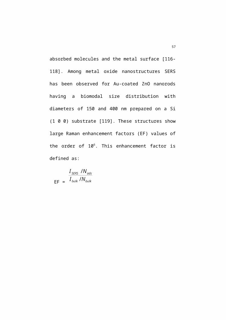
nanorods having a biomodal size distribution with diameters of 150
and 400 nm prepared on a Si (1 0 0) substrate [119]. These struc-
33
tures show large Raman enhancement factors (EF) values of the or-
der of 106. This enhancement factor is defined as:
EF =
where ISERS is the intensity of the vibrational mode in the SERS spec-
trum, Ibulk is the intensity of the same mode in the Raman spectrum
and Nads and Nbulk represent the numbers of the corresponding ana-
lytic molecules effectively excited by the laser beam [120]. Highly
surface enhanced Raman spectra have also been obtained using in-
dium tin oxide coated gold nanotriangles as well as gold nanoparti-
cles immobilized indium tin oxide [121]. Experimental reports on
ZnO crystalline samples covered with Ag-nanoparticles suggest that
the resonant Raman scattering process is assisted by metal-induced
gap states at the Ag/GaN and Ag/ZnO interfaces. This study pro-
vides a view on electron-mediated enhanced Raman scattering SERS
of lattice vibrations in oxide semiconductors [122]. The presence of
defect sites such as metal pinholes, can diminish the enhancement
[123].
34
3.4.3 Magneto-Optical Properties of Oxide Nanostructures
As will be discussed in more detail in Section V, defects in
metal oxide nanostructures can also have strong effects on the mag-
netic properties of these systems. These induced spin structures can,
in turn, affect the optical response of the nanostructures. As an ex-
ample, the formation of anti-phase boundary defects in metal oxides
can give rise to large internal strains [124]. To determine the coer-
cive field of a given sample, longitudinal MOKE magnetometry is
measured using a light source. The optical and magneto-optical
properties of oxides, such as ZnMnO, in the Faraday configuration
give us an estimate of the exchange constant [125]. In this context
we emphasize that MOKE effect is very sensitive to the strain, stoi-
chiometry, and film thickness. A large mismatch between the lattice
constants of the thin film and substrate can lead to a large residual
strain due to the formation of anti-phase boundary defects [126-
127]. In turn, these anti-phase boundary defects may subsequently
reduce the net magnetization by changing the exchange interaction
across an anti-phase boundary. The magneto-optical properties of
metal oxide nanostructures are therefore sensitive to the defect struc-
35
ture in the samples. These structural defect induced changes in the
magnetic properties can be investigated by a number of different
techniques, including magneto-optic Kerr effect (MOKE) measure-
ments [128].
Magneto-optical probes are provide a powerful tool for identify-
ing the origins of different bound exciton transitions [129]. Exciton
bound to ionized impurities can often be identified by the nonlinear
splitting of their transitions in an applied magnetic field [130-131].
Such splitting has been observed in ZnO with a magnetic field ap-
plied along the c axis. This approach can be valuable in characteriz-
ing defects in oxide nanostructures [130].
3.5 Magnetic Response
Metal oxides exhibit a very wide range of magnetic proper-
ties, ranging from ferrimagnetism with relatively large saturation
magnetizations in Fe3O4 [132], to antiferromagnetic order in NiO
[133] and CoO [134], to simple diamagnetism in ZnO [135] and
TiO2 [136], to more complex spin structures in Mn3O4 [137]. Ex-
panding this rich set of possible magnetic characteristics, it is well-

36
known that the magnetic properties of nanostructures materials are
often very different than what is observed in bulk systems [138].
Given the diverse nature of metal oxides and specific nanostructures,
there is a bewildering array of magnetic properties that are mani-
fested in metal oxide nanostructures, before even considering modi-
fications arising from defects. Rather than attempting to completely
summarize the effects of point defects on the magnetic properties of
all categories of metal oxide nanostructures, we instead consider
only specific examples of systems in which these defects can induce
weak ferromagnetic behaviour. We will first briefly discuss some
results concerning the development of superparamagnetism and
weak ferromagnetic moments in antiferromagnetic metal oxide
nanoparticles before visiting the emergence of ferromagnetic order
in diamagnetic semiconducting metal oxides induced by point de-
fects.
3.5.1 Magnetism in Metal Oxide Nanoparticles
Measurements on the weak ferromagnetism in nanoscale an-
tiferromagnetic metal oxide systems can be challenging, because of
37
the possibility of accidentally incorporating ferromagnetic secondary
phases, such metallic Co inclusions in CoO nanoparticles or thin
films [139]. Despite these difficulties, there is a growing realization
that antiferromagnetic metal oxide nanostructures often exhibit fer-
romagnetic properties that cannot necessarily be ascribed to impurity
phases [138]. The presence of surfaces (or interfaces) in antiferro-
magnetic materials can typically lead to the presence of uncompen-
sated spins arising from the incomplete cancellation of the sublattice
magnetizations in the antiferromagnetic spin structure [140]. As the
surface-to-volume ratio is exceeding large in nanostructures, the
fraction of such uncompensated spins can be a considerable fraction
of the total. In addition to such “native” uncompensated moments,
produced solely by geometrical restrictions, the inclusion of point
defects can also yield uncompensated spins, which can also exhibit
paramagnetic or weak ferromagnetic behaviour [22]. More compli-
cated magnetic effects, including the onset of multi-sublattice anti-
ferromagnetic order in nanoparticles [141] or modifications of the
electronic orbitals at the metal oxide surface [142] have also been
38
proposed, although we omit any discussion of these properties in the
following.
The magnetic properties of CoO nanoparticles are widely
studied [143-146], in part because Co/CoO core/shell nanoparticle
represent a model system for the investigation of exchange bias cou-
pling [145]. It has been found that the uncompensated moments
present in CoO can be roughly divided into two classes: those mo-
ments that are strongly coupled to the antiferromagnetic lattice and
those that are not [146]. As least a portion of spins falling in the lat-
ter category have been attributed to point defects, and these are be-
lieved to produce a paramagnetic or superparamagnetic response at
low temperatures. Similar effects have been observed in NiO
nanoparticles, which have been shown to exhibit a superparamag-
netic response that increases with decreasing particle size [147].
Careful measurements on small NiO nanoparticles find that the ef-
fective moment arising from these uncompensated spins exceeds
2000 B [148], which is considerably larger than what would be ex-
pected simply from uncompensated surface spins.

39
More generally, it has been suggested that low temperature
superparamagnetic behaviour is a general characteristic of antiferro-
magnetic metal oxide nanoparticles [138], including MnO and NiO
[149]. Measurements on both NiO and MnO nanoparticles find evi-
dence for superparamagnetic behavior, with saturation magnetiza-
tions for the ferromagnetic component on the order of a few emu/g
depending on particle size [149]. These samples show hysteretic be-
haviour at low temperatures, which vanishes at higher temperatures,
characteristic of superparamagnetism. These investigations also find
that the superparamagnetic blocking temperature increases with in-
creasing particle size for the NiO nanoparticles but, surprisingly, de-
creases with increasing size for the MnO nanoparticles [149]. This
difference in the size dependence of the magnetic properties at least
hints at the possibility that the origins for superparamagnetism in the
two samples may be different. Because weak ferromagnetism in an-
tiferromagnetic systems can arise both from discontinuities in the
magnetic structure at the surface and from point defects, it is chal-
lenging to unambiguously assign the observed superparamagnetic
moments to one mechanism or the other. Nevertheless, it is clear
40
that structural defects can significantly modify the magnetic re-
sponse in antiferromagnetic metal oxide nanostructures.
3.5.2 Ferromagnetism in Defect-Rich Semiconducting Metal Ox-
ides
A more dramatic example of how point defects can affect the
magnetic properties of metal oxides can be found in the observation
of ferromagnetism in defect-rich, intrinsically diamagnetic semicon-
ducting oxides [21, 39, 138, 150-152]. The original studies on this
class of materials highlighted the development of ferromagnetism in
metal oxide films doped with magnetic transition metal ions, in par-
ticular, Co substituted into TiO2 [153] and Mn substituted into ZnO
[154]. Measurements on this class of materials found considerable
sample-to-sample variation in the magnetic properties [155-156],
leading to suggestions that the magnetic properties were produced
by precipitates of a secondary ferromagnetic phase [157]. Further-
more, measurements on nearly stoichiometric Co and Mn doped
ZnO samples found no evidence for ferromagnetism and identified
only weak antiferromagnetic nearest-neighbor coupling between the
41
dopant ions [158-159]. Subsequent experiments on Co doped ZnO
found evidence for the crucial role played by oxygen vacancy de-
fects in the development of ferromagnetic order in this class of mate-
rials, with air annealed films (low oxygen vacancy defect concentra-
tion) having negligible magnetizations while vacuum annealed films
(high oxygen vacancy defect concentration) exhibiting distinct ferro-
magnetism [24].
Despite the recognition that point defects play an important
role in the development of ferromagnetic order in transition metal
doped semiconducting oxides, it is difficult to disentangle the effects
of defects from the contributions arising from the magnetic dopant
ions[160]. However, over the past several years it has become ap-
parent that ferromagnetism can develop in diamagnetic metal oxides,
which is believed to be driven solely by the presence of point defects
[161]. Signatures of ferromagnetic order were observed in undoped
HfO2 [151] and subsequently in a range of other metal oxides, in-
cluding TiO [39-40], In2O3 [21], ZnO [162], and CeO2 [163-164],
among many others [138, 152]. Because most of these systems do
not have thermodynamically stable magnetic compositions, it is un-
42
likely that the ferromagnetism arises from the precipitation of ferro-
magnetic impurity phases. It is found that the magnetic properties
of these systems depend strongly on the nature of the point defects
present [165], leading to suggestions of defect mediated ferromag-
netism in metal oxide nanostructures [166].
It is known that point defects in diamagnetic metal oxides
can introduce local moments [22]. The details of this local forma-
tion depend sensitively on the compound. For example, oxygen va-
cancies [167] and zinc interstitials have been predicted to be non-
magnetic in wurzite ZnO, although there are reports of Zn intersti-
tials enhancing the magnetic properties in doped ZnO [168], while
oxygen interstitials and zinc vacancies are expected to show sizeable
moments, ranging from roughly 0.2 B [167] to 2 B [67]. How-
ever, both oxygen and cerium vacancies are expected to contribute
to the magnetic moment in defect-rich CeO2 [164]. However, in the
complete absence of interactions, defect induced moments would be
expected to result in paramagnetic, rather than ferromagnetic behav-
iour, so the emergence of ferromagnetism in these metal oxide mate-
rials is rather surprising.

43
The strong connection between defects and ferromagnetism
in metal oxide nanostructures is demonstrated by studies on TiO2
thin films [25]. The as-prepared TiO2 thin films are relatively defect
free, as shown in the high resolution transmission electron mi-
croscopy images in Fig. 2d, and have a very small magnetization
(Fig. 8a). This small moment can be attributed to residual oxygen
defect vacancies that remain after air annealing [25]. Conversely,
vacuum annealed TiO2 films, presumably having a much higher con-
centration of oxygen vacancies, exhibit a much higher concentration
of defects, leading to an amorphous structure at the surface (Fig. 2e).
Introducing oxygen vacancy defects leads to a considerable en-
hancement in the magnetization. This increase depends on film
thickness, pointing to an intimate connection among microstructure,
point defects, and the emergence of ferromagnetism, and reaches 40
emu/cm3 for films having a thickness of 25 nm (Fig. 8b). Compar-
ing the size of the magnetic signal with an estimate of the total vol-
ume occupied by the surface disordered layer in the TiO2 films leads
to the suggestion that the magnetism in these samples may develop
solely in the defect-rich regions of the sample [25]. Most signifi-

44
cantly, the magnetization decreases systematically when the films
are exposed to air under ambient conditions [25], again highlighting
both the role of oxygen vacancy defects in developing magnetic or-
der and the importance of properly characterizing the stability of
point defects when considering their effects on metal oxide nanos-
tructures.
Investigations on CeO2, Al2O3, ZnO, In2O3, and SnO2 [138,
169] nanoparticles, among others, find evidence for weak ferromag-
netism, having small saturation magnetizations but clear hysteresis
loops, albeit often with almost negligible coercivities. The moments
in these nanostructured samples is very small, on the order of only
10-4 to 10-3 emu/g [138], but significantly larger than the completely
negligible magnetizations observed in diamagnetic bulk samples.
Sintering the samples at high temperatures in the presence of oxygen
completely suppresses the magnetization [138], leading to the con-
clusion that the ferromagnetism may be intimately connected with
the defect structure, specifically including oxygen vacancy defects,
at the surface of the nanoparticles. It is suggested that unpaired elec-
trons trapped on oxygen vacancies may be relevant for the develop-
45
ment of ferromagnetism and, furthermore, that such ferromagnetic
order may be a general characteristic of all metal oxide nanoparticles
[161, 166].
3.5.3 Spin Polarization in Defect-Rich Metal Oxide Nanostruc-
tures
There is considerable debate concerning the observations of
ferromagnetism in undoped metal oxide nanostructures, including
the concern that these magnetic features may arise from the acciden-
tal incorporation of ferromagnetic impurities during sample prepara-
tion or handling [160, 170]. This uncertainty arises mainly because
the very small magnetizations observed in these measurements
could, in many cases, be produced by almost negligibly small
amounts of contaminants, which could easily be missed by even the
most thorough sample characterization. It is therefore desirable to
probe the development of magnetic order in these systems using
some technique that is not sensitive to trace amounts of ferromag-
netic impurity phases. A number of different approaches to this
problem have been considered, including magnetotransport measure-
46
ments [171] and magnetic dichroism spectroscopy [172]. In the fol-
lowing, we discuss another approach based on measurements of the
charge carrier spin polarization at normal/superconducting interface
[173].
Thin films of undoped In2O3 exhibit a small but distinct fer-
romagnetic signature with the inclusion of oxygen vacancy defects,
introduced by vacuum annealing [21]. Room temperature magnetic
hysteresis loops, showing a saturation moment of 0.3±1 emu/cm3
and a coercive field of 50-200 Oe, are shown in Fig. 9a. Because
these vacuum annealed In2O3 films remain conducting to low tem-
peratures, as discussed in Section III, it is possible to probe the spin
polarization of the charge carriers using Point Contact Andreev Re-
flection (PCAR) [173]. The results of PCAR measurements made at
T=2 K with a Nb tip are shown in Fig. 9b. The zero voltage dip in
conductance is characteristic of a finite spin polarization of the In2O3
charge carriers. A more careful analysis of the conductance curve
yields an estimated spin polarization of approximately 50%, indica-
tive of ferromagnetism in these defect-rich metal oxide nanostruc-
tures [21]. While these investigations do not unambiguously prove
47
the existence of intrinsic, carrier mediated ferromagnetic order, they
do firmly establish that the measured magnetization is at least
strongly coupled to the conduction electrons. Evidence for a finite
spin polarization in Co doped ZnO films has also been inferred from
low temperature tunneling magnetoresistance measurements on
Co/Al2O3/Co:ZnO heterostructures [174].
3.5.4 Mechanisms for Magnetism in Metal Oxide Nanostructures
There are a number of proposals for the origin of weak ferro-
magnetism in defect-rich semiconducting metal oxide nanostructures
[161, 166]. As the stoichiometric parent compounds are diamag-
netic, the point defects must both provide the magnetic moments and
introduce interactions among these defect moments. While oxygen
vacancy defects are predicted to yield magnetic moments of approxi-
mately 2 B [67], this relatively small moment is insufficient to pro-
duce the high Curie temperatures, typically well above room temper-
ature [175], observed in many defect-rich metal oxide nanostruc-
tures. It has been suggested that cation defects may offer much
larger magnetic moments, leading to correspondingly larger Curie

48
temperatures [21]. For example, density functional calculations on
CeO2 find a moment of 2 B per oxygen vacancy, associated with
the Ce 4f electrons, with a much larger moment of 4 B attached to
Ce vacancies arising from O 2p orbitals [176]. Similar computations
on SnO2 find that Sn vacancies are magnetic, carrying a moment of
approximately 4 B, while oxygen vacancy defects are non-mag-
netic [177].
The presence of defect-induced magnetic moments alone is
insufficient to ferromagnetism in these semiconducting metal oxide
nanostructures; room temperature ferromagnetism requires relatively
large interactions among these moments. Local density approxima-
tion calculations on SnO2 find evidence for an oscillating exchange
interaction between moments associated with Sn vacancies (VSn),
with strong ferromagnetic coupling arising for an average separation
of 0.55 nm [177]. This exchange coupling can be modeled approxi-
mately by a Ruderman-Kittel-Kasuya-Yosida (RKKY) type interac-
tion, with a kF of 0.12 nm-1, suggesting the importance of charge car-
riers in mediating the ferromagnetism. The possible role of defect-
induced conduction electrons in promoting ferromagnetic order in
49
defect-rich metal oxides has also been discussed for In2O3 thin films
[178-179]. It has been proposed that the n-type carriers from oxy-
gen vacancy defects are highly, though not completely, compensated
by indium vacancy defects. The residual n-type charge carriers may
have a relatively high density of states at the Fermi level, due to the
quasi-localized nature of the donors, promoting high temperature
ferromagnetic order [21].
It has recently been suggested that the ferromagnetism in
metal oxide nanostructures can be produced by Stoner-type band
splitting rather than exchange coupling between local moments
[180]. This is motivated, in part, by the argument that, for reason-
able materials parameters, RKKY mediated ferromagnetic order in
these systems should develop only below 20 K. In this model, the
defects produce a density of states NS(E), with a peak lying close to
the Fermi level. The introduction of a local charge reservoir can
shift the Fermi level to align with a peak in NS(E), which can satisfy
the Stoner criterion leading to a spin-split impurity band. In this
proposal, the charge reservoir is introduced by mixed valence transi-
tion metal dopants [66], although other mechanisms are also sug-
50
gested [22, 138, 180]. In principle, metal ion vacancies, which can
act as electron acceptors, could provide the charge reservoir. This
model is particularly relevant for nanostructured metal oxide sys-
tems, as it is suggested that the ferromagnetism would arise only in
defect-rich areas or surfaces, where the defect density of states
would be large [138].
While there remains considerable uncertainty surrounding
the mechanisms giving rise to ferromagnetism in metal oxide nanos-
tructures, experimentally it is clear that weak ferromagnetism is very
generally observed in both antiferromagnetic and diamagnetic sys-
tems. Furthermore, a number of studies confirm that this magnetiza-
tion is correlated with the density of point defects, whether oxygen
vacancies, metal ion vacancies, or other. Although the saturation
magnetizations associated with this ferromagnetism is generally
small, and the coercive fields are also small or vanishing at room
temperature for superparamagnetic systems, such ferromagnetic or-
der represents an emergent property driven solely by point defects,
which is relevant for understanding how these defects modify the
behaviour of metal oxide nanostructures.
51
3.6 Defect Engineering in Metal Oxide Nanostructures
When considering defects in metal oxide nanostructures, it is
crucial to recognize that all of the negative connotations of the word
“defect” are strictly associated only with imperfections in the crystal
lattice of the system and should not prejudice the interpretation of
the induced changes in the physical properties. While lattice defects
can have a large effect on the properties of oxide materials, these
changes can be beneficial, detrimental, or neutral depending on the
specific application being considered. An enhanced conductivity
produced by charge hopping between defects sites is certainly a
drawback for a metal oxide insulating layer in a MOSFET [181-
182], but can be crucial for developing optically transparent thin
film electrodes [41]. The weak ferromagnetism arising from surface
defects in nanoparticles may offer a route to developing spintronic
devices [183], but could also produce spurious magnetic signals in
nanoscale sensors. It is, however, essential to consider the potential
effects of defect-induced properties when investigating metal oxide
52
nanostructures and to recognize the opportunities presented by de-
fects in introducing new functionalities into the system.
Controlling the defect chemistry in metal oxide nanostruc-
tures offers a route to tuning existing materials properties or incor-
porating new characteristics. This can be an attractive approach for
modifying materials, since this does not involve the addition of new
elements, which reduces the potential for the formation of spurious
secondary phases. The defect structure in nanomaterials can nor-
mally be tuned by varying the conditions during sample preparation,
or by post preparation techniques. The possibility of reversibly con-
trolling the defect structure, such as vacuum annealing to introduce
oxygen vacancy defects then annealing in an oxygen-rich environ-
ment to remove these defects, leads to a tunability that is completely
absent when controlling the materials properties by doping. How-
ever, it can be exquisitely difficult to experimentally parameterize
defect-induced properties because of problems associated with quan-
tifying the concentration of native defects. It is much more straight-
forward to measure a small percentage of Co doped into ZnO [32]
than it is to determine the degree of oxygen non-stoichiometry for
53
slightly oxygen deficient samples [59]. While simulations provide a
great deal of insight into the relationship between the concentration
of native defects and their effects on the physical properties of ox-
ides, the ability to tailor the defect structure in metal oxides for spe-
cific applications will require the development of improved tools to
more precisely parameterize the point defects in real systems.
One of the central themes of this short review is that native
point defects in oxides can lead to the emergence of completely new
materials properties that are absent in the stoichiometric parent com-
pound. Since nanostructured materials can typically develop much
higher defect concentrations than bulk systems, researchers working
with oxide nanomaterials should remain cognizant of this effect.
One further complication associated with the defect chemistry of
metal oxides arises from the fact that in some, but by no means all,
cases, the native point defects can be unstable. In some materials,
oxygen vacancy defects are removed as materials are held under am-
bient conditions, while in other systems, metal ion interstitials can
readily diffuse even at room temperature [12]. This can lead to a
very complicated time dependence for the induced physical proper-

54
ties. For example, weak ferromagnetism in oxygen deficient TiO2
vanishes after only a few hours for samples stored under ambient
conditions [25], while the magnetic signal in In2O3 films persists for
years [21]. This dynamical evolution in physical properties is likely
to be detrimental for many applications, so it is important to fully in-
vestigate the stability of defect-rich metal oxide nanostructures,
along with their response, before they can be considered for incorpo-
ration into devices.
3.7 Conclusions
We have presented a brief and somewhat idiosyncratic over-
view of defects in metal oxide nanostructures and how these defects
modify the physical properties of these systems. We have focused
primarily on native point defects in binary oxides, mainly consider-
ing only defects and interstitials. The specific nature of the most rel-
evant point defects, whether VO, MI, or other, varies considerably
among different materials, and, in many cases, remains a topic of
lively debate. Beyond perturbing the existing materials properties,
such as introducing a impurity paramagnetic response or increasing
55
the conductivity, the modifications offered by these point defects
can lead to the emergence of entirely new physical behaviour. The
presence of point defects can produce metallic conductivity, at least
over some range of temperatures, optical responses characteristic of
collective behaviour, and weak ferromagnetism. While the specific
mechanisms producing these features vary considerably from system
to system, the broad nature of the response is somewhat universal,
particularly considering the magnetic characteristics. The ability to
not only modify but build new physical properties into metal oxide
nanostructures through defect chemistry greatly expands the funca-
tionality of these materials and is expected to play a crucial role in
the next generation of oxide devices.
Acknowledgements
We have greatly benefitted from many conversations with A. Dixit,
P. Kharel, B. Nadgorny, R. Naik, V.M. Naik, R. Panguluri, R. Se-
shadri, R. Suryanarayanan, and J. Thakur. We acknowledge sup-
port from the National Science Foundation through DMR-0644823,
56
from the Jane and Frank Warchol Foundation, and from the Insti-
tute for Manufacturing Research at Wayne State University.
57
Fig. 1 Schematic illustration of possible structural defect in metal
oxides (adapted from Ref. [23])
Fig. 2 Defects in In2O3 [(a) to (c)] and TiO2 nanoparticles [(d)-(e)]
and micron sized particles [(f) – (g)]. High resolution transmission
electron micrographs of typical surface regions for (a) as-deposited
and (b) vacuum annealed In2O3 samples. (c) A magnified view of a
section of figure (b) with arrows showing typical of several distor-
tions in the crystal lattice. The square region of HRTEM in (c) corre-
sponds to a unit cell of In2O3 shown in the ball and stick model pro-
jected along (100) plane. The insets (i and ii) in (c) are the simulated
HRTEM images with (i) a oxygen vacancy and (ii) a oxygen va-
cancy with two adjacent In atoms clustering models. Bright field
TEM images show surface regions of TiO2 nanoparticles for air (d)
and vacuum (e) annealed samples. The TEM (f) and HRTEM (g)
images of vacuum-annealed sputter-deposited films show the inte-
rior of the crystallites with large number of parallel twin running
along the (0 1 1)
58
Fig. 3 Temperature dependent resistivity for an air annealed de-
fect poor In2O3 thin film (open symbols), and the same film after
vacuum annealing (defect rich, closed symbols).
Fig. 4 Optical absorption spectra for defect rich (upper curve) and
defect poor (lower curve) In2O3 thin films
Fig. 5 Logarithmic plot of low temperature PL spectrum of Ni: ZnO
grown in Ar atmosphere at 10 K.
Fig. 6 (a) PL spectra of ZnO nanorods calcined at different tempera-
tures. (b) SEM images of ZnO nanorods synthesized at different
temperatures [a more complete discussion is included
in Ref 96].
Fig. 7 A Comparison of E2 phonon shift in Raman spectra of the as-
deposited nanostructured and the bulk ZnO samples. The peak at
579 cm−1 and 381 cm−1 occurring in bulk ZnO powder are sup-
59
pressed for the brushes as well as droplets. Inset shows shift in the
peak occurring at 437 cm-1.
Fig. 8 Room temperature magnetization curves for an air annealed
defect poor TiO2 film (a) and for a vacuum annealed defect rich TiO2
film (b).
Fig. 9 (a) Room temperature magnetization curve for an oxygen de-
ficient In2O3 thin film. (b) Point contact Andreev reflection mea-
surement on the same oxygen deficient In2O3 thin film, measured at
T=2 K using a Nb tip. A fit to this curve yields an estimate spin po-
larization of P=45%.
60
References
1. Rodríguez, J.A., Fernández-García, M., eds. SYNTHESIS, PROPERTIES, AND APPLICA-TIONS OF OXIDE NANOMATERIALS. John Wiley & Sons, Inc., Hoboken, New Jersey (2007)
2. Cao, G., ed. NANOSTRUCTURES & NANOMATERIALS: Synthesis, Properties & Appli-cations Imperial College Press, London (2004)
3. Poole Jr., C.P., Owens, F.J.: Introduction to Nanotechnology. John Wiley & Sons, Inc, Hoboken, New Jersey (2003)
4. Li, M., Li, J.C.: Size effects on the band-gap of semiconductor compounds. Materials Lett. 60(20), 2526-2529 (2006)
5. Liou, S.H., et al.: Enhancement of coercivity in nanometer-size CoPt crystallites. J. App. Phys. 85(8), 4334-4336 (1999)
6. Weertman, J.R.: Mechanical behaviour of nanocrystalline metals, in Nanostructured mat-erails, processing, properties and applications, C.C. Koch, Editor. 2002, Noyes Publica-tions / William Andrew Publishing, Norwich, NY (2002)
7. Balamurugan, B., et al.: Size-dependent conductivity-type inversion in Cu2O nanoparti-cles. Phys. Rev. B 69 165419-1 (2004)
8. Hono, K., Ohnuma, M.: Microstructures and Properties of Nanocrystalline and Nanogranular Magnetic Materials. In: Nalwa, H.S. (ed.) Magnetic Nanostructures, pp. 300. American Scientific Publishers, (2002)
9. Djurisić, A.B., Leung, Y.H.: Optical Properties of ZnO Nanostructures. Small 2(8-9), 944-961 (2006)
10. Han, B. Q., Laverni, E.J., Mohamed, F.A.: MECHANICAL PROPERTIES OF NANOS-TRUCTURED MATERIALS. Rev. of Adv. Mater. Sci. 9 1-16 (2005)
11. Janotti, A., Van de Walle, C.G.,: Native point defects in ZnO. Phys. Rev. B 76(16) (2007)12. McCluskey, M. D., Jokela, S.J.: Defects in ZnO. J. App. Phys. 106(7), 071101 (2009)13. Ischenko, V., et al.: Zinc oxide nanoparticles with defects. Adv. Funct. Mater. 15, 1945-
1954 (2005)14. Janotti, A., Van de Walle, C.G.: Fundamentals of zinc oxide as a semiconductor. Rep. on
Prog. in Phys. 72, 126501 (2009)15. Diebold, U.: The surface science of titanium dioxide. Surf. Sci. Rep. 48(5-8), 53-229
(2003)16. Carel, C., Mouallem-Bahout, M., Gaude, J.: Re-examination of the non-stoichiometry and
defect structure of copper(II) oxide or tenorite, Cu1 +/- zO or CuO1 +/-epsilon - A short review. Solid State Ionics 117(1-2), 47-55 (1999)
17. Smyth, D.M.: The defect chemistry of metal oxides. Oxf. University Press (2000)18. Tilley, R. J.D.: Defects in solids. John Wiley and Sons, Inc. (2008)19. Kilic, C., Zunger, A.: Origins of coexistence of conductivity and transparency in SnO2.
Phys. Rev. Lett. 88, 095501 (2002)20. Sudakar, C., et al.: Coexistence of anion and cation vacancy defects in vacuum-annealed
In2O3 thin films. Scripta Materialia 62(2), 63-66 (2010)21. Panguluri, R.P., et al.: Ferromagnetism and spin-polarized charge carriers in In2 O3 thin
films. Phys. Rev. B 79, 165208 (2009)22. Stoneham, M.: The strange magnetism of oxides and carbons. J. Phys.: Condensed Matter
22, 074211-074218 (2010)23. Kofstad, P., Norby, T.: Defects and transport in crystalline solids. (2007)24. Sudakar, C., et al.: Raman spectroscopic studies of oxygen defects in Co-doped ZnO films
exhibiting room-temperature ferromagnetism. J. Phys.: Condensed Matter 19(2), 026212 (2007)

61
25. Sudakar, C., et al.: Room temperature ferromagnetism in vacuum-annealed TiO2 thin films. J. Magnetism and Magnetic Mater. 320(5), L31-L36 (2008)
26. Halliburton, L.E., et al.: Production of native donors in ZnO by annealing at high temper-ature in Zn vapor. App. Phys. Lett. 87(17), 172108 (2005)
27. Weber, M.H., et al.: Defect engineering of ZnO. App. Surf. Sci. 255(1), 68-70 (2008)28. Reece, M., Morrell, R.: Electron-Microscope Study of Nonstoichiometric Titania. J. Mater.
Sci. 26(20), 5566-5574 (1991)29. Erhart, P., Albe, K., Klein, A.: First-principles study of intrinsic point defects in ZnO:
Role of band structure, volume relaxation, and finite-size effects. Phys. Rev. B 73, 205203 (2006)
30. Janotti, A., Van de Walle, C.G.: Oxygen vacancies in ZnO. App. Phys. Lett. 87(12) (2005)31. Kohan, A.F., et al.: First-principles study of native point defects in ZnO. Phys. Rev. B
61(22), 15019-15027 (2000)32. Ali, B., et al.: Interplay of dopant, defects and electronic structure in driving ferromag-
netism in Co-doped oxides: TiO2, CeO2 and ZnO. J. Phys.: Condensed Matter 21(45) 456005 (2009)
33. Kim, D., et al.: The origin of oxygen vacancy induced ferromagnetism in undoped TiO2. J. Phys.: Condensed Matter 21(19) 195405 (2009)
34. Khalid, M., et al.: Defect-induced magnetic order in pure ZnO films. Phys. Rev. B 80(3), 035331 (2009)
35. von Wenckstern, H., et al.: Anionic and cationic substitution in ZnO. Prog. Solid State Chem. 37(2-3), 153-172 (2009)
36. Zhang, S.B., Wei, S.H., Zunger, A.: Intrinsic n-type versus p-type doping asymmetry and the defect physics of ZnO. Phys. Rev. B 63, 075205 (2001)
37. Cox, P.A.: Transition metal oxides. Clarendon Press, Oxford (1992)38. Catlow, C.R.A., James, R.: Disorder in TiO2-x. Proc. R. Soc. Lond. A. 384, 157-173 (1982)39. Yoon, S.D., et al.: Oxygen-defect-induced magnetism to 880 K in semiconducting anatase
TiO2-delta films. J. Phys.: Condensed Matter 18(27), L355-L361 (2006)40. Yoon, S.D., et al.: Magnetic semiconducting anatase TiO2-[delta] grown on (1 0 0)
LaAlO3 having magnetic order up to 880 K. J. Magnetism and Magnetic Mater. 309(2), 171-175 (2007)
41. Dixit, A., et al.: Undoped vacuum annealed In2O3 thin films as a transparent conducting oxide. App. Phys. Lett. 95(19) (2009)
42. Rao, C.N.R., Raveau, B.: Transition Metal Oxides. VCH Publishers Inc. (1995)43. Norton, D.P.: Synthesis and properties of epitaxial electronic oxide thin-film materials.
Mater. Sci. & Eng.: R: Rep. 43(5-6), 139-247 (2004)44. Pacchioni, G.: Ab initio theory of point defects in oxide materials: structure, properties,
chemical reactivity. Solid State Sci. 2, 161-179 (2000)45. Domaradzki, J., et al.: Transparent oxide semiconductors based on TiO2 doped with V, Co
and Pd elements. J. Non-Crystalline Solids 352, 2324-2327 (2006)46. Heluani, S.P., et al.: Electrical conductivity mechanisms in zinc oxide thin films deposited
by pulsed laser deposition using different growth environments. Thin Solid Films 515, 2379-2386 (2006)
47. Ishizuka, S., et al.: Control of hole carrier density of polycrystalline Cu2O thin films by Si doping. App. Phys. Lett. 80, 950-952 (2002)
48. Tomlins, G.W., Routbort, J.L., Mason, T.O.: Zinc self-diffusion, electrical properties, and defect structure of undoped, single crystal zinc oxide. J. App. Phys. 87, 117-123 (2000)
49. Ozgur, U., et al.: A comprehensive review of ZnO materials and devices. J. App. Phys. 98(4) (2005)
50. Morkoc, H., Ozgur, U.: Zinc Oxide. Wiley-VCH Verlag GmbH & Co., Weinheim (2009)51. Coleman, V.A., Jagdish, C.: Zinc Oxide Bulk, thin films and nanostructures. Elsevier, Ox-
ford (2006)52. Selim, F.A., et al.: Nature of Native Defects in ZnO. Phys. Rev. Lett. 99, 085502 (2007)
62
53. van de Walle, C.G.: Defect analysis and engineering in ZnO. in 21st International Confer-ence on Defects in Semiconductors. ICDS-21, 16-20 July 2001 . 2001. Netherlands: Else-vier.
54. Tomita, T., et al.: The origin of n-type conductivity in undoped In2O3. App. Phys. Lett. 87(5) (2005)
55. Hamberg, I., Granqvist, C.G.: Evaporated Sn-doped In2O3 films: Basic optical porperties and applications to energy-efficient windows. J. App. Phys. 60, R123 (1986)
56. Hartnagel, H.L., Dawar, A.K.L., Jagadish, C.: Semiconducting transparent thin films. In-stitute of Physics Publishing, Bristol (1995)
57. de Wit, J.H.W.: The high temperature behavior of In2O3. J. Solid State Chem. 13, 192 (1975)
58. Frank, G., Kostlin, G.: Electrical properties and defect model of tin-doped indium oxide layers. J. App. Phys. A 27 (1982)
59. Bellingham, J.R., Mackenzie, A.P., Phillips, W.A.: Precise measurements of oxygen con-tent: Oxygen vacancies in transparent conducting indium oxide films. App. Phys. Lett., 58, 2506-2508 (1991)
60. Agoston, P., et al.: Geometry, electronic structure and thermodynamic stability of intrinsic point defects in indium oxide. J. Phys.: Condensed Matter 21, 455801-455812 (2009)
61. Soon, A., et al.: Native defect-induced multifarious magnetism in nonstoichiometric cuprous oxide: first-principles study of bulk and surface properties of Cu2-O. Phys. Rev. B 7, 035205 (2009)
62. Jang, W.-L., et al.: Point defects in sputtered NiO films. App. Phys. Lett. 94, 062103 (2009)
63. Biju, V., Khadar, M.A.: AC conductivity of nanostructured nickel oxide. J. Mater. Sci. 36, 5779-5787 (2001)
64. Hasiguti, R.R., Yagi, E.: Electrical conductivity below 3 K of slightly reduced oxygen-defi-cient rutile TiO2-x. Phys. Rev. B 49, 7251-7256 (1994)
65. Lunkenheimer, P., et al.: Correlated barrier hopping in NiO films. Phys. Rev. B 44, 5927-5930 (1991)
66. Coey, J.M. D., et al.: Charge-transfer ferromagnetism in oxide nanoparticles. J. Phys. D 41, 134012 (2008)
67. Xu, Z., et al.: Ferromagnetism in pure wurtzite zinc oxide. J. App. Phys. 105, 507-508 (2009)
68. Henrich, V.E.: The surfaces of metal oxides. Rep. on Prog. in Phys. 48, 1481-1541 (1985)69. Munnix, S., Schmeits, M.: Electronic structure of oxygen vacancies on TiO2(110) and
SnO2(110) surfaces. in 10th International Vacuum Congress (IVC-10), 6th International Conference on Solid Surfaces (ICSS-6) and 33rd National Symposium of the American Vacuum Society, 27-31 Oct. 1986. 1987. USA.
70. Harvey, S.P., et al.: Surface versus bulk electronic/defect structures of transparent con-ducting oxides: I. Indium oxide and ITO. J. Phys. D 39, 3959-3968 (2006)
71. Niemann, D., et al.: Plasmon excitation by multiply charged Neq+ ions interacting with an Al surface. Phys. Rev. Lett. 80, 3328-3331 (1998)
72. Demangeot, F., et al.: Experimental study of LO phonons and excitons in ZnO nanoparti-cles produced by room-temperature organometallic synthesis. App. Phys. Lett. 88, 71921 (2006)
73. Pai-Chun, C., et al.: Finite size effect in ZnO nanowires. App. Phys. Lett. 90, 113101 (2007)
74. Wang, J.B., et al.: Raman scattering and high temperature ferromagnetism of Mn-doped ZnO nanoparticles. App. Phys. Lett. 88, 252502 (2006)
75. Lima, S.A.M., et al.: Luminescent properties and lattice defects correlation on zinc oxide. International J. Inorgan. Mater. 3(7), 749-754 (2001)
76. Kong, Y.C., et al.: Ultraviolet-emitting ZnO nanowires synthesized by a physical vapor deposition approach. App. Phys. Lett. 78, 407-409 (2001)
63
77. Lin, H.Y., et al.: Laser action in Tb(OH)3/SiO2 photonic crystals. Optics Express 16, 16697-16703 (2008)
78. Guichard, A. R., et al.: Tunable light emission from quantum-confined excitons in TiSi2-catalyzed silicon nanowires. Nano Lett. 6, 2140-2144 (2006)
79. Hummer, K.: Interband magnetoreflection of ZnO. Physica Status Solidi B 56, 249-260 (1973)
80. Makino, T., et al.: Band gap engineering based on MgxZn1-xO and CdyZn1-yO ternary alloy films. App. Phys. Lett. 78, 1237-1239 (2001)
81. Jin, B.J., Im, S., Lee, S.Y. : Violet and UV luminescence emitted from ZnO thin films grown on sapphire by pulsed laser deposition. Thin Solid Films 366, 107-110 (2000)
82. Bagnall, D.M., et al: Room temperature excitonic stimulated emission from zinc oxide epi-layers grown by plasma-assisted MBE. in Eighth International Conference on II-VI Com-pounds, 25-29 Aug. 1997. Elsevier, Netherlands (1998)
83. Bylander, E.G.: Surface effects on the low-energy cathodoluminescence of zinc oxide. J. App. Phys. 49, 1188-1195 (1978)
84. Garces, N.Y., et al.: Role of copper in the green luminescence from ZnO crystals. App. Phys. Lett. 81, 622-624 (2002)
85. Prosanov, I.Y., Politov, A.A.: Surface effects on the low-energy cathodoluminescence of zinc oxide. Inorg. Mater. 31, 663 (1995)
86. Egehaaf, J.H., Oelkrug, D.: Luminescence and nonradiative deactivation of excited states involving oxygen defect centers in polycrystalline ZnO. J. Cryst. Growth 161, 190-194 (1996)
87. Vanheusden, K., et al.: Mechanisms behind green photoluminescence in ZnO phosphor powders. J. App. Phys. 79, 7983-7990 (1996)
88. Zhou, H., Cai, W., Zhang, L.: Photoluminescence of indium-oxide nanoparticles dispersed within pores of mesoporous silica. App. Phys. Lett. 75, 495-497 (1999)
89. Soares, J.W., et al.: Novel photoluminescence properties of surface-modified nanocrys-talline zinc oxide: Toward a reactive scaffold. Langmuir 24, 371-374 (2008)
90. Mo, C.M., et al.: Enhancement effect of photoluminescence in assemblies of nano-ZnO particles/silica aerogels. J. App. Phys. 83, 4389-4391 (1998)
91. Singh, S., Rao, M.S.R.: Optical and electrical resistivity studies of isovalent and aliova-lent 3d transition metal ion doped ZnO. Phys. Rev. B 80, 045210-045220 (2009)
92. Godlewski, M.: ODMR study of the nature of iron-red photoluminescence in ZnS crystals. Solid State Communications 47, 811-813 (1983)
93. Goldewski, M., Skowronski, M.: Effective deactivation of the ZnS visible photolumines-cence by iron impurities. Phys. Rev. B 32, 4007-4013 (1985)
94. Mang, A., Reimann, K., Rubenacke, S.: Band gaps, crystal-field splitting, spin-orbit cou-pling, and exciton binding energies in ZnO under hydrostatic pressure. Solid State Com-munications 94, 251-254 (1995)
95. Singh, S., et al.: Investigation of low-temperature excitonic and defect emission from Ni-doped ZnO nanoneedles and V-doped ZnO nanostructured film. New J. Phys. 12 023007-023018 (2010)
96. van Dijken, A., et al.: The Kinetics of the Radiative and Nonradiative Processes in Nanocrystalline ZnO Particles upon Photoexcitation. The J. Phys. Chem. B 104(8), 1715-1723 (2000)
97. Ginley, D.S., Bright, C.: Transparent conducting oxides. MRS Bulletin 25, 15-21 (2000)98. Dai, L., et al.: Fabrication and characterization of In2O3 nanowires. App. Phys. A A75,
687-689 (2002)99. Ng, Y.H., et al.: Fabrication of hollow carbon nanospheres encapsulating platinum
nanoparticles using a photocatalytic reaction. Adv. Mater. 19, 597-601 (2007)100. Soulantica, K., et al.: Synthesis of indium and indium oxide nanoparticles from indium cy-
clopentadienyl precursor and their application for gas sensing. Adv. Functional Mater. 13, 553-557 (2003)
64
101. Lee, M.S., et al.: Characterization of the oxidized indium thin films with thermal oxida-tion. Thin Solid Films 279, 1-3 (1996)
102. Wu, P., et al.: Synthesis and photoluminescence property of indium oxide nanowires. App. Surf. Sci. 255, 3201-3204 (2008)
103. Singh, S., et al.: Formation of ZnO nanobrushes in direct atmosphere using a carbon cata-lyst and A Zn metal source. Nano 3, 361-365 (2008)
104. Yang, J.H., et al.: Low temperature hydrothermal growth and optical properties of ZnO nanorods. Cryst. Res. Technology 44, 87-91 (2009)
105. Ashkenov, N., et al.: Infrared dielectric functions and phonon modes of high-quality ZnO films. J. App. Phys. 93 126-133 (2003)
106. Yang, Y.H., et al.: Radial ZnO nanowire nucleation on amorphous carbons. App. Phys. Lett. 87, 183109-1 (2005)
107. Yang, R.D., et al.: Photoluminescence and micro-Raman scattering in ZnO nanoparticles: The influence of acetate adsorption. Chem. Phys. Lett. 411, 150-154 (2005)
108. Rajalakshmi, M., et al.: Optical phonon confinement in zinc oxide nanoparticles. J. App. Phys. 87, 2445-2448 (2000)
109. Alim, K.A., Fonoberov, V.A., Balandin, A. A.: Origin of the optical phonon frequency shifts in ZnO quantum dots. App. Phys. Lett. 86, 53103-1 (2005)
110. Bundesmann, C., et al.: Raman scattering in ZnO thin films doped with Fe, Sb, Al, Ga, and Li. App. Phys. Lett. 83, 1974-1976 (2003)
111. Manjon, F.J., et al.: Silent Raman modes in zinc oxide and related nitrides. J. App. Phys. 97, 53516-1 (2005).
112. Kostic, R., et al.: Low-frequency Raman scattering from ZnO(Fe) nanoparticles. Acta Physica Polonica A 116, 65-67 (2009)
113. Zhang, P., Guo, Y.: Surface-Enhanced Raman Scattering inside Metal Nanoshells. J. Am. Chem. Soc. 131(11), 3808-3809 (2009)
114. Hirsch, L.R., et al.: A whole blood immunoassay using gold nanoshells. Analytical Chem. 75, 2377-2381 (2003)
115. Jackson, J.B., et al.: Controlling the surface enhanced Raman effect via the nanoshell ge-ometry. App. Phys. Lett. 82, 257-259 (2003)
116. Albrecht, M. G., Creighton, J. A.: J. Am. Chem. Soc. 84 (1977)117. Chao, S., et al.: A double substrate sandwich structure for fiber surface enhanced Raman
scattering detection. App. Phys. Lett. 92, 103107 (2008)118. Yi, Z., et al.: Liquid core photonic crystal fiber sensor based on surface enhanced Raman
scattering. App. Phys. Lett. 90, 193504 (2007)119. Gu, Y., et al.: Quantum confinement in ZnO nanorods. App. Phys. Lett. 85, 3833 (2004)120. Sakano, T., et al.: Surface enhanced Raman scattering properties using Au-coated ZnO
nanorods grown by two-step, off-axis pulsed laser deposition. J. Phys. D41 (2008)121. Pettinger, B.: Light scattering by adsorbates at Ag particles: quantum-mechanical ap-
proach for energy transfer induced interfacial optical processes involving surface plas-mons, multipoles, and electron-hole pairs. J. Chem. Phys. 85, 7442-7451 (1986)
122. Liu, C.Y., et al.: Anomalously enhanced Raman scattering from longitudinal optical phonons on Ag-nanoparticle-covered GaN and ZnO. App. Phys. Lett. 96, 033109 (2010)
123. Cullum, B., et al.: Characterization of multilayer-enhanced surface-enhanced raman scat-tering (SERS) substrates and their potential for SERS nanoimaging. NanoBioTechnology 3(1), 1-11 (2007)
124. Habermeier, H.U.: Strategies towards controlling strain-induced mesoscopic phase sepa-ration in manganite thin films. J. Phys.: Condensed Matter 20(43), 434228 (2008)
125. Przezdziecka, E.: Optical and magnetooptical properties of the p-type ZnMnO. E-MRS Fall Meeting Symposium F (2006)
126. Arora, S.K., et al.: Antiphase boundaries induced exchange coupling in epitaxial Fe3O4 thin films. J. Magnetism and Magnetic Mater. 286, 463-467 (2005)
65
127. Eerenstein, W., et al.: Origin of the increased resistivity in epitaxial Fe3O4 films. Phys. Rev. B 66, 201101 (2002)
128. Siang Huei, L., Jian Ping, W., Teck Seng., L.: Study of in-depth defects using magneto-op-tical Kerr effect by measuring the magnetic hardness coefficient in magnetic thin films . in INTERMAG 2000 Digest of Technical Papers. 2000 IEEE International Magnetics Con-ference, 9-13 April 2000 USA: IEEE (2000)
129. Thomas, D.G. and J.J. Hopfield, Optical Properties of Bound Exciton Complexes in Cad-mium Sulfide. Phys. Rev. 128(5), 2135 (1962)
130. Loose, P., Rosenzweig, M., Wöhlecke, M.: Zeeman Effect of Bound Exciton Complexes in ZnO. physica status solidi (b) 75(1),137-144 (1976)
131. Reynolds, D.C., Litton, C.W. Collins, T.C.: Zeeman Effects in the Edge Emission and Ab-sorption of ZnO. Phys. Rev. 140(5A), A1726 (1965)
132. Margulies, D.T., et al.: Origin of the anomalous magnetic behavior in single crystal Fe3O4 films. Phys. Rev. Lett. 79, 5162-5165 (1997)
133. Barbier, A., et al.: Surface and bulk spin ordering of antiferromagnetic materials: NiO(111). Phys. Rev. Lett. 93, 257208-2572081 (2004)
134. Tang, Y.J., et al.: Finite size effects on the moment and ordering temperature in antiferro-magnetic CoO layers. Phys. Rev. B 67, 54408-1 (2003)
135. Kapilashrami, M., et al.: Transition from ferromagnetism to diamagnetism in undoped ZnO thin films. App. Phys. Lett. 95, 033104 (2009)
136. Khaibullin, R.I., et al.: Formation of anisotropic ferromagnetic response in rutile (TiO2) implanted with cobalt ions. Nucl. Instrum. Methods in Phys. Res., Section B 257, 369-373 (2007)
137. Dwight, K., Menyuk, N.: Magnetic Properties of Mn3O4 and the Canted Spin Problem. Physical Review 119(5), 1470 (1960)
138. Sundaresan, A., et al.: Ferromagnetism as a universal feature of nanoparticles of the oth-erwise nonmagnetic oxides. Phys. Rev. B, 74, 161306 (2006)
139. Riveiro, J.M., et al.: CoO1- layers in a reactively sputtered exchange-bias system. New J. Phys. 10, 083028 (2008)
140. Mishra, S.R., et al.: Anomalous magnetic properties of mechanically milled cobalt oxide nanoparticles. J. Nanosci. and Nanotechnol. 5, 2076-2081 (2005)
141. Jagodic, M., et al.: Surface-spin magnetism of antiferromagnetic NiO in nanoparticle and bulk morphology. J. Phys.: Condensed Matter 21, 215302 (2009)
142. Morales, M.A., et al.: Surface anisotropy and magnetic freezing of MnO nanoparticles. Phys. Rev. B75, 134423-1 (2007)
143. Gruyters, M.: Spin-glass-like behavior in CoO nanoparticles and the origin of exchange bias in Layered CoO/ferromagnet structures. Phys. Rev. Lett. 95, 077204-1 (2005)
144. Tomou, A., et al.: Weak ferromagnetism and exchange biasing in cobalt oxide nanoparti-cle systems. J. App. Phys. 99, 123915-1 (2006)
145. Tracy, J.B., Bawendi, M. G.: Defects in CoO in oxidized cobalt nanoparticles dominate exchange biasing and exhibit anomalous magnetic properties. Phys. Rev. B 74, 184434-1 (2006)
146. Tracy, J.B., et al.: Exchange biasing and magnetic properties of partially and fully oxi-dized colloidal cobalt nanoparticles. Phys. Rev. B 72, 64404-1 (2005)
147. Richardson, J.T., et al.: Origin of superparamagnetism in nickel oxide. J. App. Phys, 70, 6977-6982 (1991)
148. Makhlouf, S.A., et al.: Magnetic anomalies in NiO nanoparticles. in 41st Annual Confer-ence on Magnetism and Magnetic Materials, 12-15 Nov. 1996. 1997. USA: AIP.
149. Ghosh, M., et al.: MnO and NiO nanoparticles: synthesis and magnetic properties. J. Mater. Chem. 16, 106-111 (2006)
150. Coey, J.M.D.: High-temperature ferromagnetism in dilute magnetic oxides. J. App. Phys. 97(10) (2005)
151. Coey, J. M.D., et al.: Magnetism in hafnium dioxide. Phys. Rev. B 72, 024450 (2005)
66
152. Hong, N.H., et al.: Room-temperature ferromagnetism observed in undoped semiconduct-ing and insulating oxide thin films. Phys. Rev. B 73, 132404 (2006)
153. Matsumoto, Y., et al.: Room-Temperature Ferromagnetism in Transparent Transition Metal-Doped Titanium Dioxide. Sci. 291(5505), 854-856 (2001)
154. Sharma, P., et al.: Ferromagnetism above room temperature in bulk and transparent thin films of Mn-doped ZnO. Nat. Mater. 2(10), 673-677 (2003)
155. Prellier, W., Fouchet, A., Mercey, B.: Oxide-diluted magnetic semiconductors: a review of the experimental status. J. Phys.: Condensed Matter 15(37), R1583-R1601 (2003)
156. Liu, C., Yun, F. Morkoc, H.: Ferromagnetism of ZnO and GaN: A review. J. Mater. Sci.: Mater. Electron. 16(9), 555-597 (2005)
157. Park, J.H., et al.: Co-metal clustering as the origin of ferromagnetism in Co-doped ZnO thin films. App. Phys. Lett. 84(8), 1338-1340 (2004)
158. Rao, C.N.R., Deepak, F.L.: Absence of ferromagnetism in Mn- and Co-doped ZnO. J. Mater. Chem. 15(5), 573-578 (2005)
159. Lawes, G., et al.: Absence of ferromagnetism in Co and Mn substituted polycrystalline ZnO. Phys. Rev. B 71, 045201 (2005)
160. Abraham, D.W., Frank, M.M., Guha, S.: Absence of magnetism in hafnium oxide films. App. Phys. Lett. 87(25), 252502 (2005)
161. Coey, J.M.D., Dilute magnetic oxides. Curr. Opin. in Solid State & Mater. Science 10(2) 83-92 (2006)
162. Hong, N.H., Sakai, J., Brize, V.: Observation of ferromagnetism at room temperature in ZnO thin films. J. Phys.: Condensed Matter 19(3), 036219 (2007)
163. Liu, Y.L., et al.: Size dependent ferromagnetism in cerium oxide (CeO2) nanostructures independent of oxygen vacancies. J. Phys.: Condensed Matter 20(16), 165201 (2008)
164. Han, X., Lee, J., Yoo, H.-I.: Oxygen-vacancy-induced ferromagnetism in CeO2 from first principles. Phys. Rev. B 79, 100403 (2009)
165. Song, Y.Q., et al.: Direct evidence of oxygen vacancy mediated ferromagnetism of Co doped CeO2 thin films on Al2O3(0001) substrates. J. Phys.: Condensed Matter 20(33), 255510 (2008)
166. Coey, J.M.D., d0 ferromagnetism. Solid State Sciences 7(6),660-667 (2005)167. Kim, D., Yang, J.-H., Hong, J.: Ferromagnetism induced by Zn vacancy defect and lattice
distortion in ZnO. J. App. Phys. 106(1) 013908 (2009)168. Lau, S.P., et al.: Zn-interstitial-enhanced ferromagnetism in Cu-doped ZnO films. J. Mag-
netism and Magnetic Mater. 315, 107-110 (2007)169. Kharel, P., et al.: Room temperature ferromagnetism in Cr-doped In2O3 on high vacuum
annealing of thin films and bulk samples. J. App. Phys. 101(9) (2007)170. Potzger, K., Zhou, S.: Non-DMS related ferromagnetism in transition metal doped zinc ox-
ide. physica status solidi (b) 246(6), 1147-1167 (2009)171. PARK, Y.D., et al.: Anomalous hall effect in wide bandgap diluted magnetic semiconduc-
tors co-doped with non-magnetic impurities. Proceedings - Electrochemical Soc. 6, 300-311 (2004)
172. Ney, A., et al.: Absence of Intrinsic Ferromagnetic Interactions of Isolated and Paired Co Dopant Atoms in Zn1-xCoxO with High Structural Perfection. Phys. Rev. Lett. 100, 157201 (2008)
173. Soulen, R.J., Jr., et al.: Measuring the Spin Polarization of a Metal with a Superconduct-ing Point Contact. Sci. 282(5386), 85-88 (1998)
174. Qingyu, X., et al.: Spin manipulation in co-doped ZnO. Phys. Rev. Lett. 101, 076601-1 (2008)
175. Ueda, K., Tabata, H., Kawai, T.: Magnetic and electric properties of transition-metal-doped ZnO films. App. Phys. Lett. 79, 988-990 (2001)
176. Fernandes, V., et al.: Dilute-defect magnetism: origin of magnetism in nanocrystalline CeO2. Phys. Rev. B 80, 035202 (2009)
67
177. Rahman, G., Garcia-Suarez, V.M., Soon Cheol, H.: Vacancy-induced magnetism in SnO2: a density functional study. Phys. Rev. B 78, 184404 (2008)
178. Philip, J., et al.: Carrier-controlled ferromagnetism in transparent oxide semiconductors. Nat. Mater. 5, 298-304 (2006)
179. Raebiger, H., Lany, S. Zunger, A.: Control of ferromagnetism via electron doping in In2O3: Cr. Phys. Rev. Lett. 101 (2008)
180. Coey, J.M.D., Venkatesan, M., Fitzgerald, C. B.: Donor impurity band exchange in dilute ferromagnetic oxides. Nat. Mater. 4(2), 173-179 (2005)
181. Hutin, L., et al.: GeOI pMOSFETs scaled down to 30-nm gate length with record off-state current. IEEE Electron Device Lett. 31(3), 234-236 (2010)
182. Qiang, F., Wagner, T.: Interaction of nanostructured metal overlayers with oxide surfaces. Surf. Sci. Rep. 62, 431-498 (2007)
183. Wolf, S.A., et al.: Spintronics: a spin-based electronics vision for the future. Sci. 294, 1488-1495 (2001)