Embed Size (px)
DESCRIPTION
UHiFET – A New High-Frequency High-Voltage Device
Citation preview
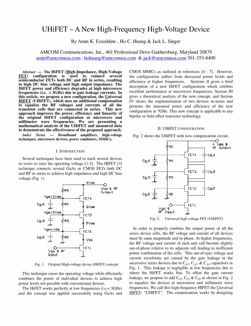
UHiFET – A New High-Frequency High-Voltage Device
By Amin K. Ezzeddine , Ho C. Huang & Jack L. Singer
AMCOM Communications, Inc., 401 Professional Drive Gaithersburg, Maryland 20879
[email protected] , [email protected] & [email protected] 301-353-8400
Abstract — The HiFET (High-Impedance, High-Voltage
FET) configuration is used to connect several semiconductor FETs both DC and RF in series, resulting in high DC bias voltage and high output impedance. The HiFET power and efficiency degrades at high microwave frequencies (i.e. > 3GHz) due to gate leakage currents. In this article, we propose a new configuration, the Universal HiFET (UHiFET), which uses an additional compensation to equalize the RF voltages and currents of all the transistor cells that are connected in series. This new approach improves the power, efficiency and linearity of the original HiFET configuration at microwave and millimeter wave frequencies. We are presenting a mathematical analysis of the UHiFET and measured data to demonstrate the effectiveness of the proposed approach.
Index Terms — Broadband amplifiers, high-voltage techniques, microwave devices, power combiners, MMICs.
I. INTRODUCTION
Several techniques have been used to stack several devices
in series to raise the operating voltage [1-3]. The HIFET [3]
technique connects several GaAs or CMOS FETs both DC
and RF in series to achieve high impedance and high DC bias
voltage (Fig. 1).
Fig. 1. Original High-voltage device (HiFET) concept
This technique raises the operating voltage while efficiently
combines the power of individual devices to achieve high
power levels not possible with conventional devices.
The HiFET works perfectly at low frequencies (i.e.< 3GHz)
and the concept was applied successfully using GaAs and
CMOS MMICs as outlined in references [4 - 7]. However,
the configuration suffers from decreased power levels and
efficiency at higher frequencies. Sections II gives a brief
description of a new HiFET configuration which exhibits
excellent performance at microwave frequencies, Section III
gives a theoretical analysis of the new concept, and Section
IV shows the implementation of two devices in-series and
presents the measured power and efficiency of the new
configuration at 7GHz. This new concept is applicable to any
bipolar or field effect transistor technology.
II. UHIFET CONFIGURATION
Fig. 2 shows the UHiFET with new compensation circuit.
Fig. 2. Universal high voltage FET (UHiFET)
In order to properly combine the output power of all the
series device cells, the RF voltage and current of all devices
must be same magnitude and in-phase. At higher frequencies,
the RF voltage and current of each unit cell become slightly
out-of-phase relative to its adjacent cell leading to inefficient
power combination of the cells. This out-of-sync voltage and
current waveforms are caused by the gate leakage in the
successive series devices due to Cg,2, C g,3 & C g,4 capacitors in
Fig. 1. This leakage is negligible at low frequencies this is
where the HiFET works fine. To offset the gate current
leakage, we propose to add Cd2, Cd3 & Cd4 as shown in Fig. 2
to equalize the devices at microwave and millimeter wave
frequencies. We call this high-frequency HIFET the Universal
HIFET: “UHIFET”. The compensation works by designing
Cd,2 to conduct a current equal to the gate current of FET2 ,
and Cd,3 , Cd,4 to equalize the gate currents of FET3 and FET4
respectively.
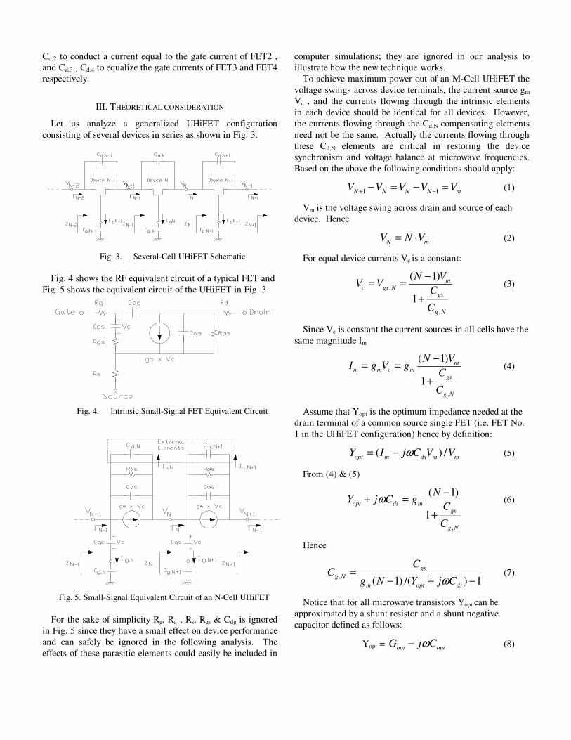
III. THEORETICAL CONSIDERATION
Let us analyze a generalized UHiFET configuration
consisting of several devices in series as shown in Fig. 3.
Fig. 3. Several-Cell UHiFET Schematic
Fig. 4 shows the RF equivalent circuit of a typical FET and
Fig. 5 shows the equivalent circuit of the UHiFET in Fig. 3.
Fig. 4. Intrinsic Small-Signal FET Equivalent Circuit
Fig. 5. Small-Signal Equivalent Circuit of an N-Cell UHiFET
For the sake of simplicity Rg, Rd , Rs, Rgs & Cdg is ignored
in Fig. 5 since they have a small effect on device performance
and can safely be ignored in the following analysis. The
effects of these parasitic elements could easily be included in
computer simulations; they are ignored in our analysis to
illustrate how the new technique works.
To achieve maximum power out of an M-Cell UHiFET the
voltage swings across device terminals, the current source gm
Vc , and the currents flowing through the intrinsic elements
in each device should be identical for all devices. However,
the currents flowing through the Cd,N compensating elements
need not be the same. Actually the currents flowing through
these Cd,N elements are critical in restoring the device
synchronism and voltage balance at microwave frequencies.
Based on the above the following conditions should apply:
1 1N N N N mV V V V V
+ −− = − = (1)
Vm is the voltage swing across drain and source of each
device. Hence
N m
V N V= ⋅ (2)
For equal device currents Vc is a constant:
,
,
( 1)
1
mc gs N
gs
g N
N VV V
C
C
−= =
+
(3)
Since Vc is constant the current sources in all cells have the
same magnitude Im
,
( 1)
1
mm m c m
gs
g N
N VI g V g
C
C
−= =
+
(4)
Assume that Yopt is the optimum impedance needed at the
drain terminal of a common source single FET (i.e. FET No.
1 in the UHiFET configuration) hence by definition:
( ) /opt m ds m m
Y I j C V Vω= − (5)
From (4) & (5)
,
( 1)
1
opt ds mgs
g N
NY j C g
C
C
ω−
+ =
+
(6)
Hence
,( 1) /( ) 1
gs
g N
m opt ds
CC
g N Y j Cω
=
− + −
(7)
Notice that for all microwave transistors Yopt can be
approximated by a shunt resistor and a shunt negative
capacitor defined as follows:
Yopt = opt opt
G j Cω− (8)
Usually Copt ≈ Cds so from (7) & (8)
,( 1) /( ) 1
( 1) / 1
gs
g N
m opt opt ds
gs
m opt
CC
g N G j C j C
C
g N G
ω ω
=
− − + −
≅
− −
(9)
Referring to Fig. 5 from Kirchhoff’s current law the current
IN coming from the Nth cell is:
,( )N m c d N ds m
I g V j C j C Vω ω= − + (10)
That same current should be sinking into the (N+1)th cell
that is:
, 1( )N m c gs c d N ds m
I g V j C V j C j C Vω ω ω+
= + − + (11)
From (10) & (11)
, 1 ,d N m d N m gs cj C V j C V j C Vω ω ω
+= + (12)
Equ. (12) simply states that for perfect synchronization the
current of the Cd,N+1 compensating capacitor is needed to feed
the compensating capacitor of the Nth cell (i.e. Cd,N) and the
gate current of the (N+1)th cell. From (12) & (3):
, 1 ,
,
( 1)
1
d N d N gsgs
g N
Nj C j C j C
C
C
ω ω ω+
−= +
+
(13)
From (13) & (6)
, 1 , /d N d N gs opt m
j C j C j C G gω ω ω+
≅ + (14)
Since Cd,1 = 0
, 1
gs
d N opt
m
j Cj C NG
g
ω
ω+
≅ (15)
From (2) & (11) we could calculate the admittance
presented at the drain of every cell YN:
,
,
1/
( ) / /
/ /
N N
opt ds d N
opt d N
Y Z
G j C N j C N
Y N j C N
ω ω
ω
=
≅ − −
≅ −
(16)
From (16) we deduct that the optimum impedance for the
Nth-Cell UHiFET is N times the optimum impedance of a
single device in parallel with a negative capacitance equal to
Cd,N/N.
The above analysis of the UHiFET shows how to improve
the HiFET to obtain good power and efficiency at any
frequency in the microwave and millimeter wave spectrum.
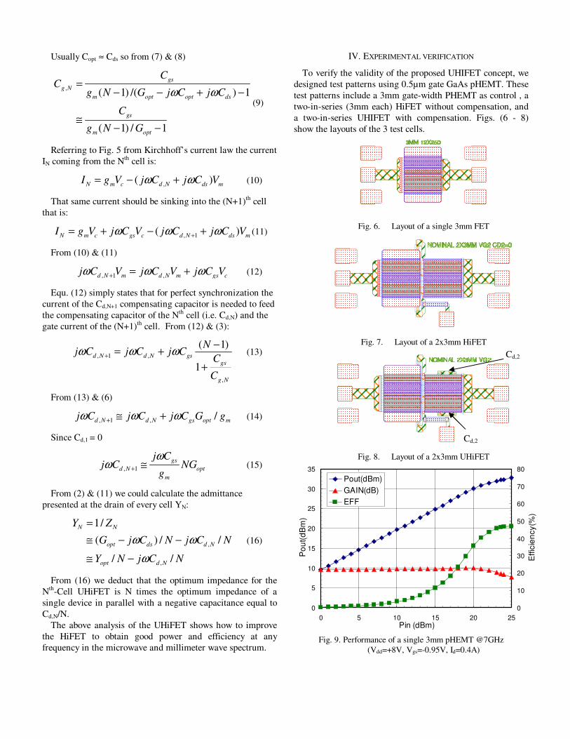
IV. EXPERIMENTAL VERIFICATION
To verify the validity of the proposed UHIFET concept, we
designed test patterns using 0.5µm gate GaAs pHEMT. These
test patterns include a 3mm gate-width PHEMT as control , a
two-in-series (3mm each) HiFET without compensation, and
a two-in-series UHIFET with compensation. Figs. (6 - 8)
show the layouts of the 3 test cells.
Fig. 6. Layout of a single 3mm FET
Fig. 7. Layout of a 2x3mm HiFET
Fig. 8. Layout of a 2x3mm UHiFET
0
5
10
15
20
25
30
35
0 5 10 15 20 25Pin (dBm)
Po
ut(
dB
m)
0
10
20
30
40
50
60
70
80
Effic
ien
cy(%
)
Pout(dBm)
GAIN(dB)
EFF
Fig. 9. Performance of a single 3mm pHEMT @7GHz
(Vdd=+8V, Vgs=-0.95V, Id=0.4A)
Cd,2
Cd,2
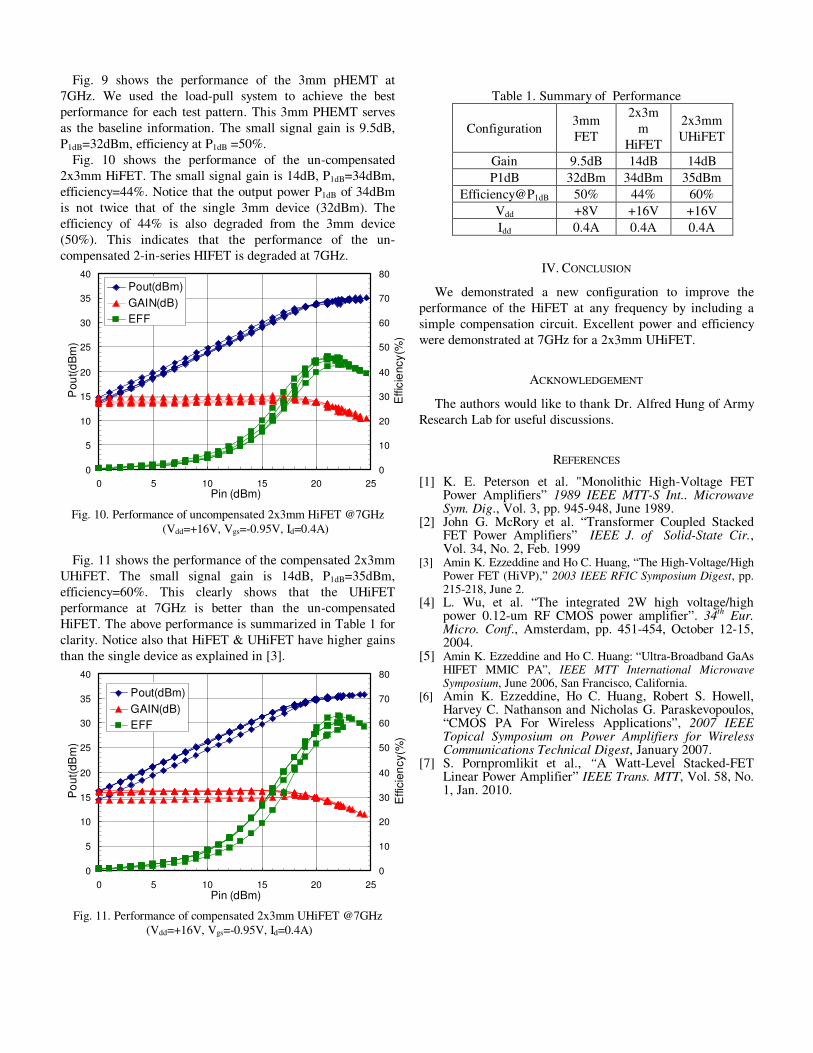
Fig. 9 shows the performance of the 3mm pHEMT at
7GHz. We used the load-pull system to achieve the best
performance for each test pattern. This 3mm PHEMT serves
as the baseline information. The small signal gain is 9.5dB,
P1dB=32dBm, efficiency at P1dB =50%.
Fig. 10 shows the performance of the un-compensated
2x3mm HiFET. The small signal gain is 14dB, P1dB=34dBm,
efficiency=44%. Notice that the output power P1dB of 34dBm
is not twice that of the single 3mm device (32dBm). The
efficiency of 44% is also degraded from the 3mm device
(50%). This indicates that the performance of the un-
compensated 2-in-series HIFET is degraded at 7GHz.
0
5
10
15
20
25
30
35
40
0 5 10 15 20 25Pin (dBm)
Po
ut(
dB
m)
0
10
20
30
40
50
60
70
80
Effic
ien
cy(%
)
Pout(dBm)
GAIN(dB)
EFF
Fig. 10. Performance of uncompensated 2x3mm HiFET @7GHz
(Vdd=+16V, Vgs=-0.95V, Id=0.4A)
Fig. 11 shows the performance of the compensated 2x3mm
UHiFET. The small signal gain is 14dB, P1dB=35dBm,
efficiency=60%. This clearly shows that the UHiFET
performance at 7GHz is better than the un-compensated
HiFET. The above performance is summarized in Table 1 for
clarity. Notice also that HiFET & UHiFET have higher gains
than the single device as explained in [3].
0
5
10
15
20
25
30
35
40
0 5 10 15 20 25Pin (dBm)
Po
ut(
dB
m)
0
10
20
30
40
50
60
70
80
Effic
ien
cy(%
)
Pout(dBm)
GAIN(dB)
EFF
Fig. 11. Performance of compensated 2x3mm UHiFET @7GHz
(Vdd=+16V, Vgs=-0.95V, Id=0.4A)
Table 1. Summary of Performance
Configuration 3mm
FET
2x3m
m
HiFET
2x3mm
UHiFET
Gain 9.5dB 14dB 14dB
P1dB 32dBm 34dBm 35dBm
Efficiency@P1dB 50% 44% 60%
Vdd +8V +16V +16V
Idd 0.4A 0.4A 0.4A
IV. CONCLUSION
We demonstrated a new configuration to improve the
performance of the HiFET at any frequency by including a
simple compensation circuit. Excellent power and efficiency
were demonstrated at 7GHz for a 2x3mm UHiFET.
ACKNOWLEDGEMENT
The authors would like to thank Dr. Alfred Hung of Army
Research Lab for useful discussions.
REFERENCES
[1] K. E. Peterson et al. "Monolithic High-Voltage FET Power Amplifiers” 1989 IEEE MTT-S Int.. Microwave Sym. Dig., Vol. 3, pp. 945-948, June 1989.
[2] John G. McRory et al. “Transformer Coupled Stacked FET Power Amplifiers” IEEE J. of Solid-State Cir., Vol. 34, No. 2, Feb. 1999
[3] Amin K. Ezzeddine and Ho C. Huang, “The High-Voltage/High Power FET (HiVP),” 2003 IEEE RFIC Symposium Digest, pp. 215-218, June 2.
[4] L. Wu, et al. “The integrated 2W high voltage/high power 0.12-um RF CMOS power amplifier”. 34
th Eur.
Micro. Conf., Amsterdam, pp. 451-454, October 12-15, 2004.
[5] Amin K. Ezzeddine and Ho C. Huang: “Ultra-Broadband GaAs HIFET MMIC PA”, IEEE MTT International Microwave Symposium, June 2006, San Francisco, California.
[6] Amin K. Ezzeddine, Ho C. Huang, Robert S. Howell, Harvey C. Nathanson and Nicholas G. Paraskevopoulos, “CMOS PA For Wireless Applications”, 2007 IEEE Topical Symposium on Power Amplifiers for Wireless Communications Technical Digest, January 2007.
[7] S. Pornpromlikit et al., “A Watt-Level Stacked-FET Linear Power Amplifier” IEEE Trans. MTT, Vol. 58, No. 1, Jan. 2010.