Embed Size (px)
Citation preview
Data Sheet Graphics
SED1742/44
June 1997
CMOS 160-BIT SEGMENT DRIVERHIGH VOLTAGE LCD DRIVER
■ DESCRIPTION
The SED1742/SED1744 is a 160 dot matrix LCD segment (column) driver for driving high-capacityLCD panels at duty cycles higher than 1/100 (up to 1/500). The LSI features a wide range of LCDvoltages. The upper and lower LCD drive voltages (V0, V5) are independent of the chip supplies.This enables the LCD drive bias voltages to be supplied from an external source. The device usesa daisy-chain enable system which decreases power consumption and eliminates the need forseparate enable signals for each driver.
The SED1742/44 is used in conjunction with the SED1743 (160-bit common driver) to drive alarge-capacity dot matrix LCD panel.
■ FEATURES
¥ Low-power high-speed CMOS technology
¥ 160-bit segment (column) driver
¥ High-speed data bus ................................4-bit (SED1742)
8-bit (SED1744)
¥ Duty cycle .................................................1/100 to 1/500
¥ Adjustable LCD drive voltages
¥ Unbiased display off function
¥ Adjustable offset bias of the LCD according to VDDH and GND
¥ Shift clock frequency ................................12MHz max at VDD = 5V
¥ Ability to adjust offset bias of the LCD source from VDD
¥ Daisy chain enable support
¥ No enable signal by controller is required
¥ Wide range of LCD voltage ......................14 to 40V
¥ Supply voltage..........................................2.7 to 5.5V
¥ Package....................................................TAB (TOA)
Au bump (D1B)
S-MOS Systems, Inc. ¥ 150 River Oaks Parkway ¥ San Jose, CA 95134 ¥ Tel: (408) 922-0200 ¥ Fax: (408) 922-0238439-1.0 1
SED1742/44
June 1997
■ SYSTEM BLOCK DIAGRAM
SED1742SED1742
LCDCONTR
320 SEG ´ 480 COMDUTY: 1/480
SED1743
SED1743
160160
160
D0~D3 , D0~D7 (SED1744)
XSCL
YSCL
YD
LP, FR
160
SED1743 160
S-MOS Systems, Inc. ¥ 150 River Oaks Parkway ¥ San Jose, CA 95134 ¥ Tel: (408) 922-0200 ¥ Fax: (408) 922-0238 439-1.02
SED1742/44
June 1997
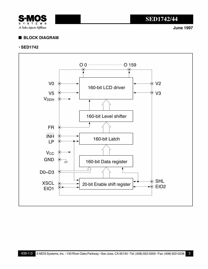
■ BLOCK DIAGRAM
¥ SED1742
V0��
V5�VDDH�
����
FR��
INH�LP�
�VCC�
GND��
D0~D3��
XSCL�EIO1
V2��V3����������������SHL�EIO2
O 0 O 159
160-bit LCD driver
160-bit Level shifter
160-bit Latch
160-bit Data register
20-bit Enable shift register
S-MOS Systems, Inc. ¥ 150 River Oaks Parkway ¥ San Jose, CA 95134 ¥ Tel: (408) 922-0200 ¥ Fax: (408) 922-0238439-1.0 3
SED1742/44
June 1997
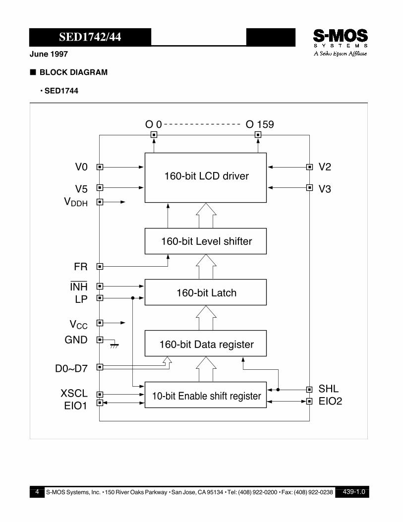
■ BLOCK DIAGRAM
¥ SED1744
V0��
V5�VDDH�
����
FR��
INH�LP�
�VCC�
GND��
D0~D7��
XSCL�EIO1
V2��V3����������������SHL�EIO2
O 0 O 159
160-bit LCD driver
160-bit Level shifter
160-bit Latch
160-bit Data register
10-bit Enable shift register
S-MOS Systems, Inc. ¥ 150 River Oaks Parkway ¥ San Jose, CA 95134 ¥ Tel: (408) 922-0200 ¥ Fax: (408) 922-0238 439-1.04
SED1742/44
June 1997
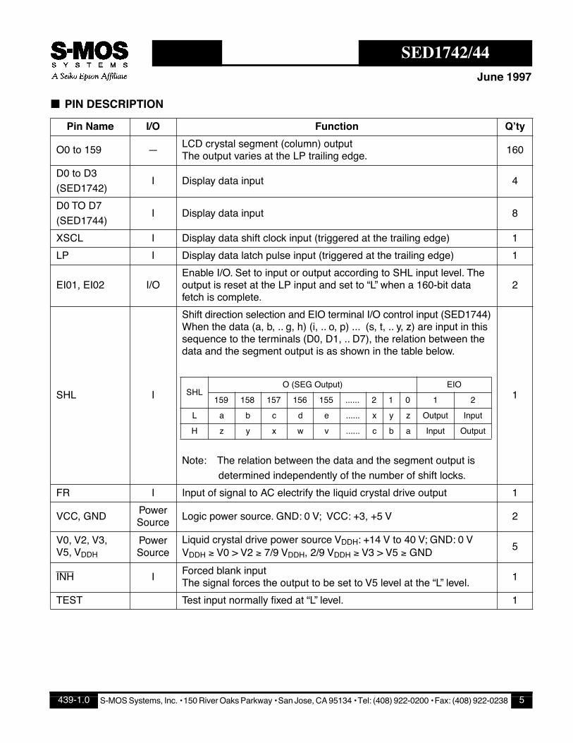
■ PIN DESCRIPTION
Pin Name I/O Function QÕty
O0 to 159 ÑLCD crystal segment (column) outputThe output varies at the LP trailing edge.
160
D0 to D3
(SED1742)I Display data input 4
D0 TO D7
(SED1744)I Display data input 8
XSCL I Display data shift clock input (triggered at the trailing edge) 1
LP I Display data latch pulse input (triggered at the trailing edge) 1
EI01, EI02 I/OEnable I/O. Set to input or output according to SHL input level. The output is reset at the LP input and set to ÒLÓ when a 160-bit data fetch is complete.
2
SHL I
Shift direction selection and EIO terminal I/O control input (SED1744)When the data (a, b, .. g, h) (i, .. o, p) ... (s, t, .. y, z) are input in this sequence to the terminals (D0, D1, .. D7), the relation between the data and the segment output is as shown in the table below.
Note: The relation between the data and the segment output is
determined independently of the number of shift locks.
1
FR I Input of signal to AC electrify the liquid crystal drive output 1
VCC, GNDPower Source
Logic power source. GND: 0 V; VCC: +3, +5 V 2
V0, V2, V3, V5, VDDH
Power Source
Liquid crystal drive power source VDDH: +14 V to 40 V; GND: 0 V VDDH ³ V0 > V2 ³ 7/9 VDDH, 2/9 VDDH ³ V3 > V5 ³ GND
5
INH IForced blank inputThe signal forces the output to be set to V5 level at the ÒLÓ level.
1
TEST Test input normally Þxed at ÒLÓ level. 1
SHLO (SEG Output) EIO
159 158 157 156 155 ...... 2 1 0 1 2
L a b c d e ...... x y z Output Input
H z y x w v ...... c b a Input Output
S-MOS Systems, Inc. ¥ 150 River Oaks Parkway ¥ San Jose, CA 95134 ¥ Tel: (408) 922-0200 ¥ Fax: (408) 922-0238439-1.0 5
SED1742/44
June 1997
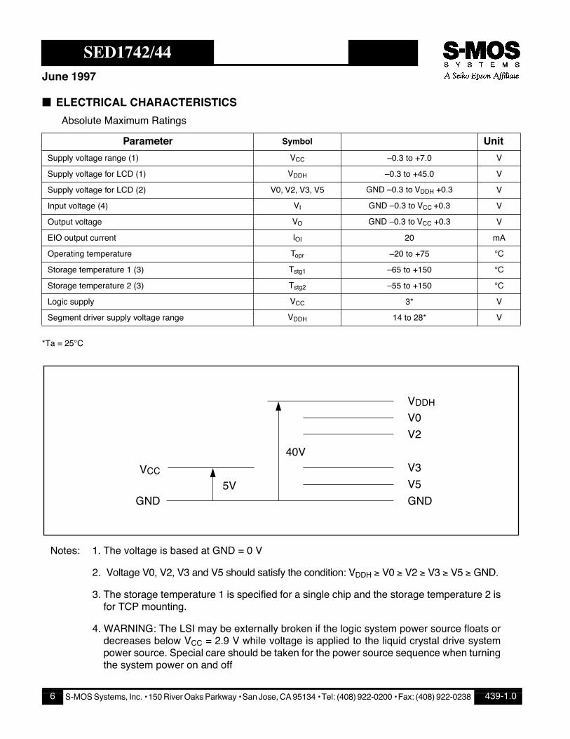
■ ELECTRICAL CHARACTERISTICS
Absolute Maximum Ratings
*Ta = 25°C
Notes: 1. The voltage is based at GND = 0 V
2. Voltage V0, V2, V3 and V5 should satisfy the condition: VDDH ³ V0 ³ V2 ³ V3 ³ V5 ³ GND.
3. The storage temperature 1 is specified for a single chip and the storage temperature 2 isfor TCP mounting.
4. WARNING: The LSI may be externally broken if the logic system power source floats ordecreases below VCC = 2.9 V while voltage is applied to the liquid crystal drive systempower source. Special care should be taken for the power source sequence when turningthe system power on and off
Parameter Symbol Unit
Supply voltage range (1) VCC Ð0.3 to +7.0 V
Supply voltage for LCD (1) VDDH Ð0.3 to +45.0 V
Supply voltage for LCD (2) V0, V2, V3, V5 GND Ð0.3 to VDDH +0.3 V
Input voltage (4) VI GND Ð0.3 to VCC +0.3 V
Output voltage VO GND Ð0.3 to VCC +0.3 V
EIO output current IOI 20 mA
Operating temperature Topr Ð20 to +75 °C
Storage temperature 1 (3) Tstg1 Ð65 to +150 °C
Storage temperature 2 (3) Tstg2 Ð55 to +150 °C
Logic supply VCC 3* V
Segment driver supply voltage range VDDH 14 to 28* V
VCC
GND
VDDH�
V0�
V2�
�
V3�
V5�
GND5V
40V
S-MOS Systems, Inc. ¥ 150 River Oaks Parkway ¥ San Jose, CA 95134 ¥ Tel: (408) 922-0200 ¥ Fax: (408) 922-0238 439-1.06
SED1742/44
June 1997
● DC Electrical Characteristics
Parameter Symbol Condition Terminal Min Typ Max Unit
Logic supply voltage (1) VCC VCC 3.0 5.0 5.5 V
Operation voltage recommended
VDDH VDDH 14.0 Ñ 40.0 V
Segment driver input supply voltage
VDDH Function VDDH 8.0 Ñ Ñ V
Segment driver input supply voltage (2)
V0 Value recommended V0 VDDH Ð2.5 Ñ VDDH V
Segment driver input supply voltage (2)
V2 Value recommended V2 7/9VDDH Ñ Ñ V
Segment driver input supply voltage (2)
V3, V5 Value recommended V3, V5 GND Ñ 2/9VDDH V
High-level input voltage
VIH
VCC = 3.0 to 5.5 V
EIO1, EIO2,D0 to D3:SED1742 D0 to D7:SED1744 XSCL, LP,
SHL, FR, INH
0.8VCC Ñ Ñ V
Low-level input voltage
VIL Ñ Ñ 0.2VCC V
High-level output voltage
VOH
VCC = 3 to 5.5 V
IOH = Ð0.6 mA
EIO1, EIO2
VCC Ð0.4 Ñ Ñ V
Low-level utput voltage
VOL IOL = 0.6 mA Ñ 0.4 V
Low-level input
leakage currentILI GND £ VIN £ VCC
D0 to D3:SED1742 D0 to D7:SED1744
LP, FR, XSCL,SHL, INH
Ñ Ñ 2.0 mA
Input: leakage current output
ILI/O GND £ VIN £ VCC EIO1, EIO2 Ñ Ñ 5.0 mA
Static current IGND VDDH = 14.0 to 40.0 V
VIH = VCC, VIL = GNDGND Ñ Ñ 25 mA
Output resistance RSEG
DVON= 0.5V condition recommended
VDDH=+30.0VO0 to O159
Ñ 0.9 2.5 kW
VDDH=+20.0V Ñ 1.0 3.0
.
S-MOS Systems, Inc. ¥ 150 River Oaks Parkway ¥ San Jose, CA 95134 ¥ Tel: (408) 922-0200 ¥ Fax: (408) 922-0238439-1.0 7
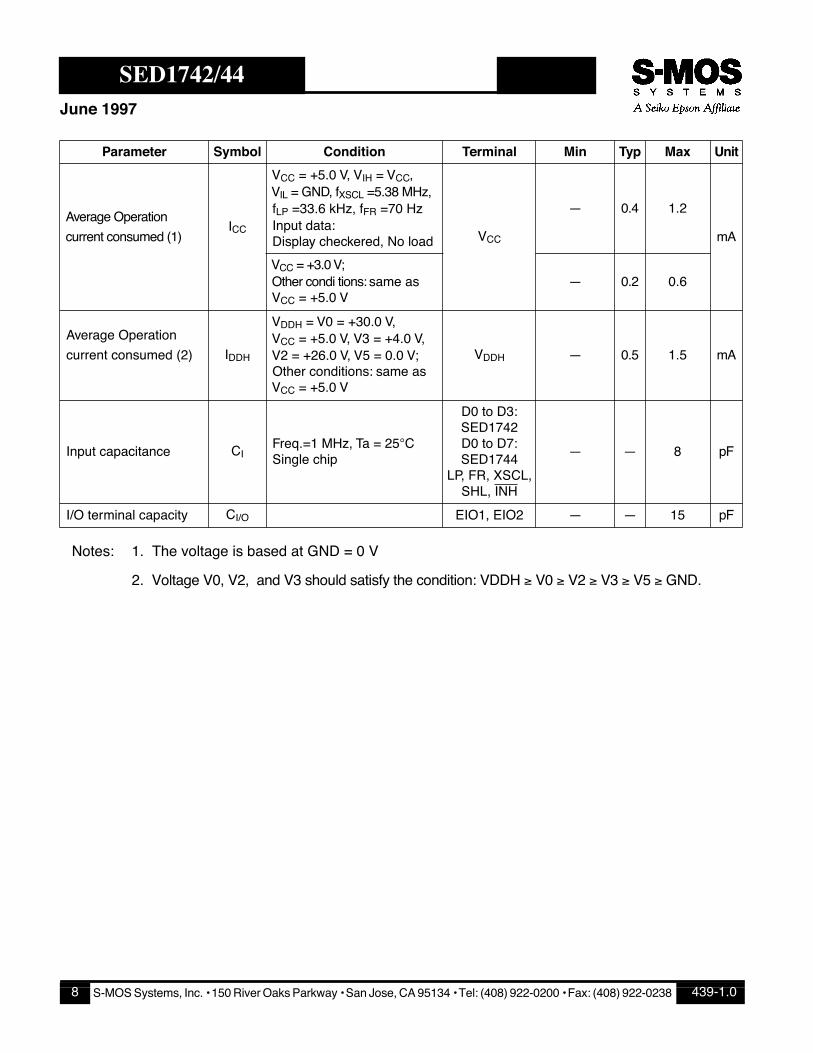
SED1742/44June 1997
Notes: 1. The voltage is based at GND = 0 V
2. Voltage V0, V2, and V3 should satisfy the condition: VDDH ³ V0 ³ V2 ³ V3 ³ V5 ³ GND.
Average Operation
current consumed (1)ICC
VCC = +5.0 V, VIH = VCC, VIL = GND, fXSCL =5.38 MHz, fLP =33.6 kHz, fFR =70 Hz Input data: Display checkered, No load VCC
Ñ 0.4 1.2
mA
VCC = +3.0 V; Other condi tions: same as VCC = +5.0 V
Ñ 0.2 0.6
Average Operation
current consumed (2) IDDH
VDDH = V0 = +30.0 V, VCC = +5.0 V, V3 = +4.0 V, V2 = +26.0 V, V5 = 0.0 V; Other conditions: same as VCC = +5.0 V
VDDH Ñ 0.5 1.5 mA
Input capacitance CI Freq.=1 MHz, Ta = 25°C Single chip
D0 to D3:SED1742 D0 to D7:SED1744
LP, FR, XSCL,SHL, INH
Ñ Ñ 8 pF
I/O terminal capacity CI/O EIO1, EIO2 Ñ Ñ 15 pF
Parameter Symbol Condition Terminal Min Typ Max Unit
S-MOS Systems, Inc. ¥ 150 River Oaks Parkway ¥ San Jose, CA 95134 ¥ Tel: (408) 922-0200 ¥ Fax: (408) 922-0238 439-1.08
SED1742/44June 1997
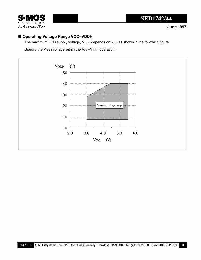
● Operating Voltage Range VCCÐVDDHThe maximum LCD supply voltage, VDDH depends on VCC as shown in the following figure.
Specify the VDDH voltage within the VCCÐVDDH operation.
50�
40�
30�
20�
10�
02.0 3.0 4.0 5.0 6.0
VCC (V)
VDDH (V)
Operation voltage range
S-MOS Systems, Inc. ¥ 150 River Oaks Parkway ¥ San Jose, CA 95134 ¥ Tel: (408) 922-0200 ¥ Fax: (408) 922-0238439-1.0 9
SED1742/44June 1997
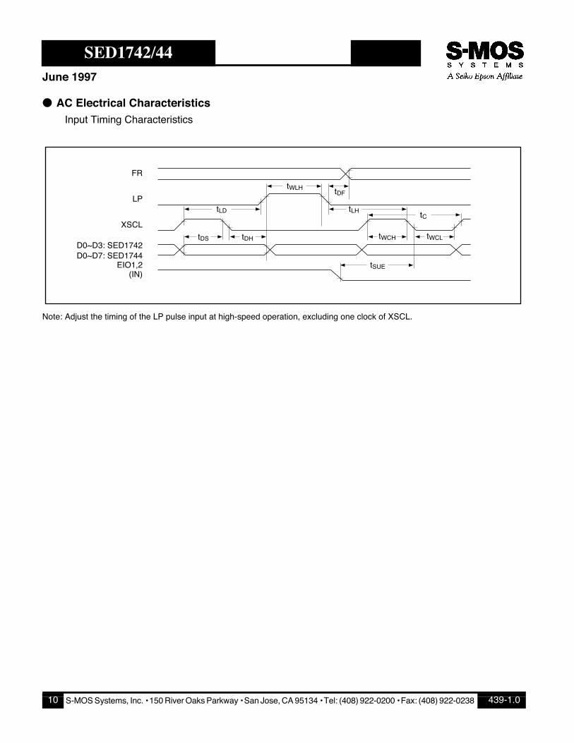
● AC Electrical Characteristics Input Timing Characteristics
Note: Adjust the timing of the LP pulse input at high-speed operation, excluding one clock of XSCL.
tWLH tDF
tLHtC
tWCLtWCHtDHtDS
tSUE
tLD
FR�
LP�
XSCL�
D0~D3: SED1742�D0~D7: SED1744�
EIO1,2�(IN)
S-MOS Systems, Inc. ¥ 150 River Oaks Parkway ¥ San Jose, CA 95134 ¥ Tel: (408) 922-0200 ¥ Fax: (408) 922-0238 439-1.010
SED1742/44June 1997
(VCC = 5.0 V ±10%, Ta = Ð20 to 75°C)
Note: tWLH defines the time duration when the LP is ÒHÓ and the XSCL is ÒLÓ
(VCC = 3.0 to 4.5 V, Ta = Ð20 to 75°C)
Note: tWLH defines the time duration when the LP is ÒHÓ and the XSCL is ÒLÓ
Parameter Symbol Condition Min Typ Max Unit
XSCL cycle tC 83 Ñ Ñ ns
XSCL high-level pulse width tWCH 30 Ñ Ñ ns
XSCL low-level pulse width tWCL 30 Ñ Ñ ns
Data setup time tDS 30 Ñ Ñ ns
Data hold time tDH 30 Ñ Ñ ns
XSCL ---> LP rise time tLD Ð5 Ñ Ñ ns
LP ---> XSCL breaking time tLH 60 Ñ Ñ ns
LP high-level pulse width (1) tWLH 45 Ñ Ñ ns
Parameter Symbol Condition Min Typ Max Unit
XSCL cycle tC 125 Ñ Ñ ns
XSCL high-level pulse width tWCH 50 Ñ Ñ ns
XSCL low-level pulse width tWCL 50 Ñ Ñ ns
Data setup time tDS 50 Ñ Ñ ns
Data hold time tDH 30 Ñ Ñ ns
XSCL ---> LP rise time tLD 0 Ñ Ñ ns
LP ---> XSCL breaking time tLH 120 Ñ Ñ ns
LP high-level pulse width (1) tWLH 90 Ñ Ñ ns
FR delay allowance time tDF Ð600 Ñ 600 ns
EIO setup time tSUE 70 Ñ Ñ ns
S-MOS Systems, Inc. ¥ 150 River Oaks Parkway ¥ San Jose, CA 95134 ¥ Tel: (408) 922-0200 ¥ Fax: (408) 922-0238439-1.0 11
SED1742/44June 1997
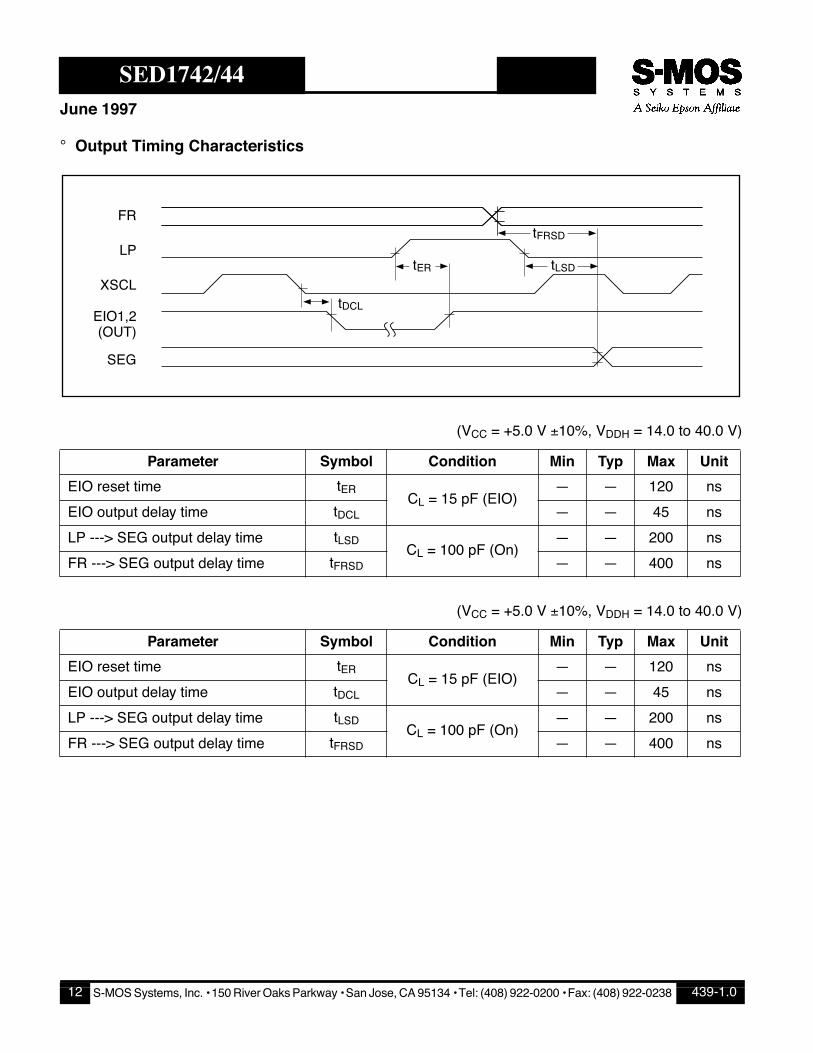
° Output Timing Characteristics
(VCC = +5.0 V ±10%, VDDH = 14.0 to 40.0 V)
(VCC = +5.0 V ±10%, VDDH = 14.0 to 40.0 V)
Parameter Symbol Condition Min Typ Max Unit
EIO reset time tERCL = 15 pF (EIO)
Ñ Ñ 120 ns
EIO output delay time tDCL Ñ Ñ 45 ns
LP ---> SEG output delay time tLSDCL = 100 pF (On)
Ñ Ñ 200 ns
FR ---> SEG output delay time tFRSD Ñ Ñ 400 ns
Parameter Symbol Condition Min Typ Max Unit
EIO reset time tERCL = 15 pF (EIO)
Ñ Ñ 120 ns
EIO output delay time tDCL Ñ Ñ 45 ns
LP ---> SEG output delay time tLSDCL = 100 pF (On)
Ñ Ñ 200 ns
FR ---> SEG output delay time tFRSD Ñ Ñ 400 ns
tLSD
tDCL
tFRSD
FR�
LP�
XSCL��
EIO1,2�(OUT)�
SEG
tER
S-MOS Systems, Inc. ¥ 150 River Oaks Parkway ¥ San Jose, CA 95134 ¥ Tel: (408) 922-0200 ¥ Fax: (408) 922-0238 439-1.012
SED1742/44June 1997
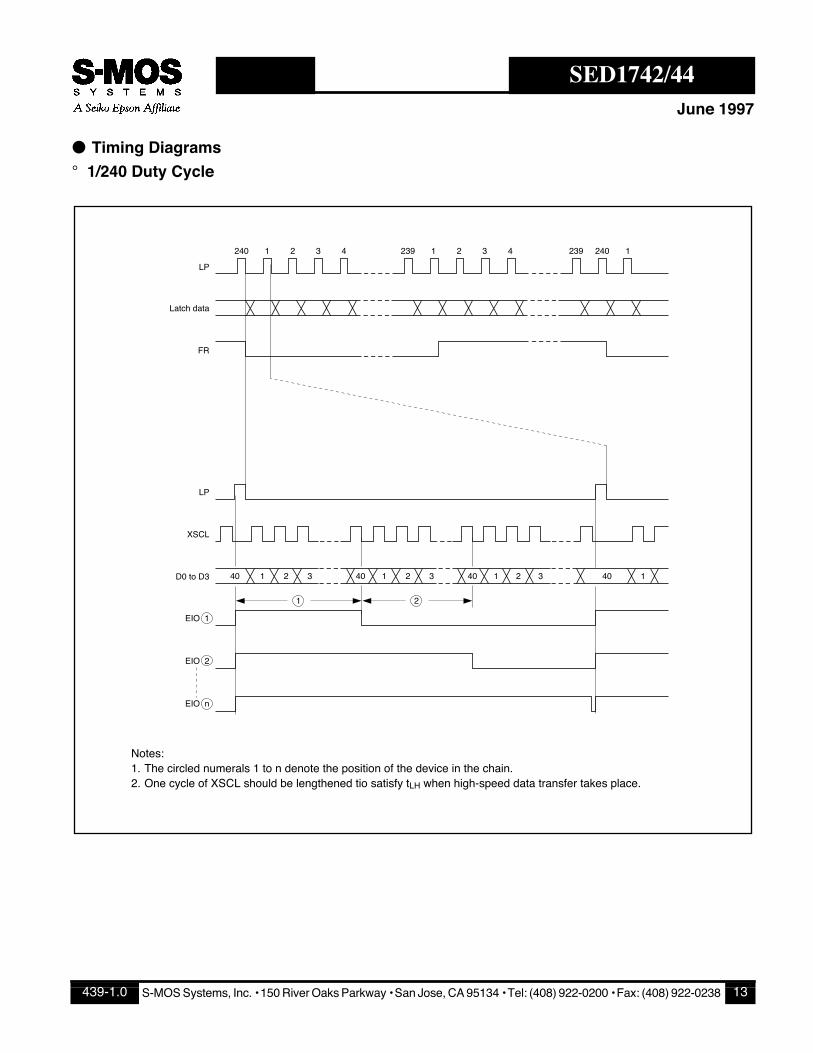
● Timing Diagrams
° 1/240 Duty Cycle
40
1
240
LP
LP
XSCL
D0 to D3
EIO 1
EIO 2
EIO n
Latch data
FR
1 2 3 4 239 1 240239 12 3 4
1 2 3 40 1 2 3 40 1 2 3 40 1
2
Notes:1.2.
The circled numerals 1 to n denote the position of the device in the chain.One cycle of XSCL should be lengthened tio satisfy tLH when high-speed data transfer takes place.
S-MOS Systems, Inc. ¥ 150 River Oaks Parkway ¥ San Jose, CA 95134 ¥ Tel: (408) 922-0200 ¥ Fax: (408) 922-0238439-1.0 13
SED1742/44June 1997
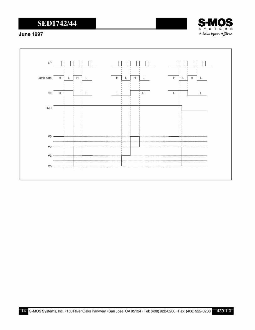
LP
Latch data H L H L
H L
H L H L
H L
H L H L
L HFR
INH
V0
V2
V3
V5
S-MOS Systems, Inc. ¥ 150 River Oaks Parkway ¥ San Jose, CA 95134 ¥ Tel: (408) 922-0200 ¥ Fax: (408) 922-0238 439-1.014
SED1742/44June 1997
■ FUNCTIONAL DESCRIPTION
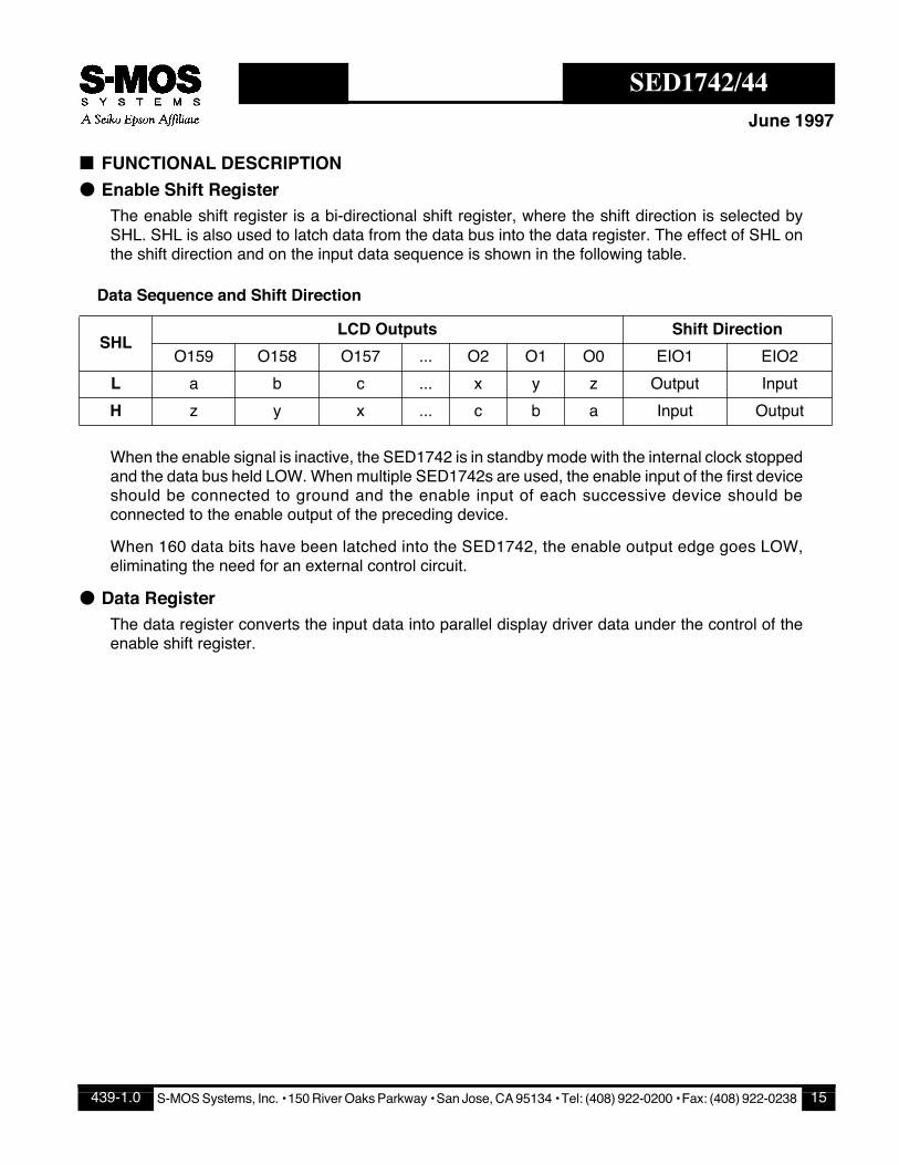
● Enable Shift RegisterThe enable shift register is a bi-directional shift register, where the shift direction is selected bySHL. SHL is also used to latch data from the data bus into the data register. The effect of SHL onthe shift direction and on the input data sequence is shown in the following table.
Data Sequence and Shift Direction
When the enable signal is inactive, the SED1742 is in standby mode with the internal clock stoppedand the data bus held LOW. When multiple SED1742s are used, the enable input of the first deviceshould be connected to ground and the enable input of each successive device should beconnected to the enable output of the preceding device.
When 160 data bits have been latched into the SED1742, the enable output edge goes LOW,eliminating the need for an external control circuit.
● Data RegisterThe data register converts the input data into parallel display driver data under the control of theenable shift register.
SHLLCD Outputs Shift Direction
O159 O158 O157 ... O2 O1 O0 EIO1 EIO2
L a b c ... x y z Output Input
H z y x ... c b a Input Output
S-MOS Systems, Inc. ¥ 150 River Oaks Parkway ¥ San Jose, CA 95134 ¥ Tel: (408) 922-0200 ¥ Fax: (408) 922-0238439-1.0 15
SED1742/44June 1997
■ APPLICATION NOTES
● Voltage LevelsThe recommended method of generating the LCD drive voltages, V0 to V5, is with a voltage dividerbetween VDDH and VGND, buffered with voltage followers.
The lower drive level, V5, is not necessarily at VGND, and separate pins are used for the voltagelevels when op-amps are used. A maximum voltage differential between V5 and VGND of 2.5V isrecommended since the driver efficiency decreases as the differential increases. Connect V5 toGND when not using op-amps.
The resistances of the voltage divider resistors should be as low as possible and within powersupply constraints.
Note that fluctuations in IDDH can cause dips in the VDDH supply. The device will be damaged if thevoltage dips below the point where the relationship VDDH (V0) ³ V2 ³ V3 ³ V5 ³ VGND breaks down.A stabilized power supply may be required when using the resistor network.
● Data LatchThe data latch latches the data into the level shifter on the falling edge of LP.
● Level ShifterThe level shifter converts the logic-level signals from the latch into the LCD driver input voltagelevels.
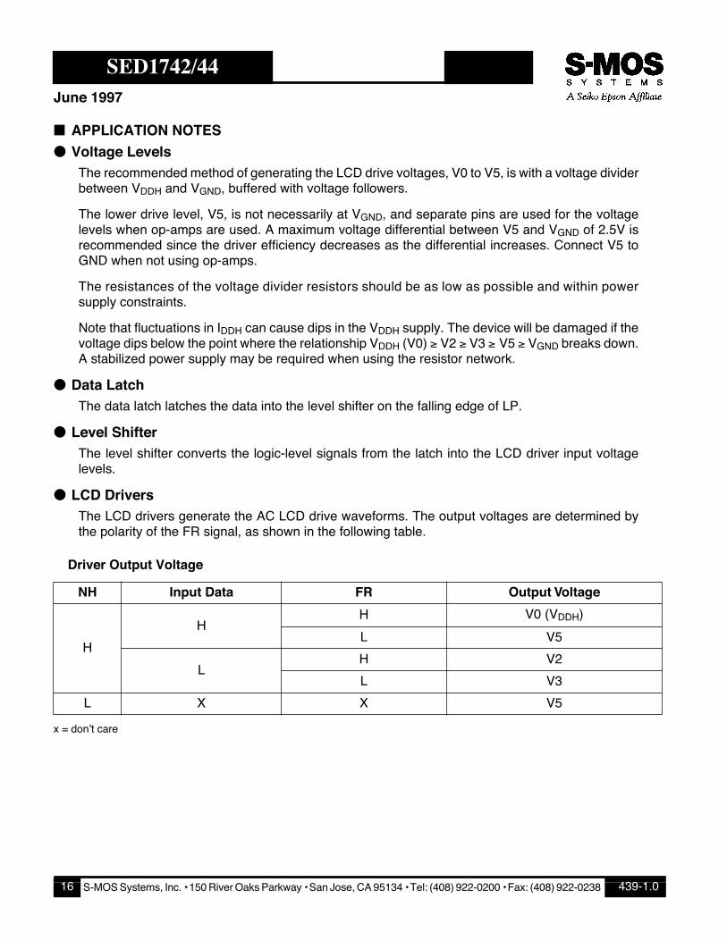
● LCD DriversThe LCD drivers generate the AC LCD drive waveforms. The output voltages are determined bythe polarity of the FR signal, as shown in the following table.
Driver Output Voltage
x = donÕt care
NH Input Data FR Output Voltage
H
HH V0 (VDDH)
L V5
LH V2
L V3
L X X V5
S-MOS Systems, Inc. ¥ 150 River Oaks Parkway ¥ San Jose, CA 95134 ¥ Tel: (408) 922-0200 ¥ Fax: (408) 922-0238 439-1.016
SED1742/44June 1997
● Power-Up and Power-Down PrecautionsAs the driver circuitry operates at high voltage, care should be taken when applying and removingpower to the SED1742 to prevent damage. If the driver supply is applied when the logic supply iseither not connected or below 2.9V, excess current will flow into the SED1742 and damage thedevice. Normal operation is guaranteed if the correct power-up and power-down sequences arefollowed.
Power-Up Sequence:Power should be applied to VCC before, or at the same time as, power is applied to thedriver circuitry.
Power-Down Sequence:Power should be removed from VCC after, or at the same time as, power is removed fromthe driver circuitry.
The SED1742 can also be damaged if the LCD output drivers start operating before the driver sup-plies stabilize. INH should be held LOW to hold the driver outputs at V5 until the driver supplieshave stabilized.
As an extra precaution, insert a fast-blow fuse in series with the driver supply.
S-MOS Systems, Inc. ¥ 150 River Oaks Parkway ¥ San Jose, CA 95134 ¥ Tel: (408) 922-0200 ¥ Fax: (408) 922-0238439-1.0 17
SED1742/44June 1997
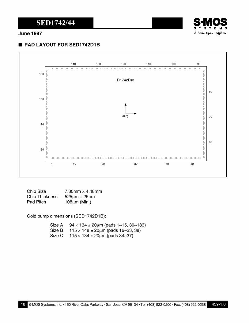
■ PAD LAYOUT FOR SED1742D1B
Chip Size 7.30mm ´ 4.48mmChip Thickness 525mm ± 25mmPad Pitch 108mm (Min.)
Gold bump dimensions (SED1742D1B):
Size A 94 ´ 134 ± 20mm (pads 1~15, 39~183)Size B 115 ´ 148 ± 20mm (pads 16~33, 38)Size C 115 ´ 134 ± 20mm (pads 34~37)
1 10 20 30 40 50
60
70
80
90100110120130140
150
160
170
180
D1742D1B
(0,0)
S-MOS Systems, Inc. ¥ 150 River Oaks Parkway ¥ San Jose, CA 95134 ¥ Tel: (408) 922-0200 ¥ Fax: (408) 922-0238 439-1.018
SED1742/44June 1997
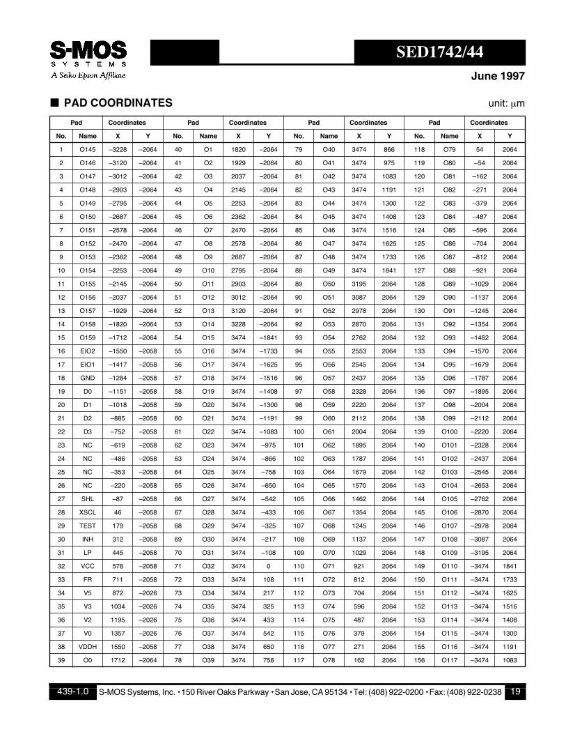
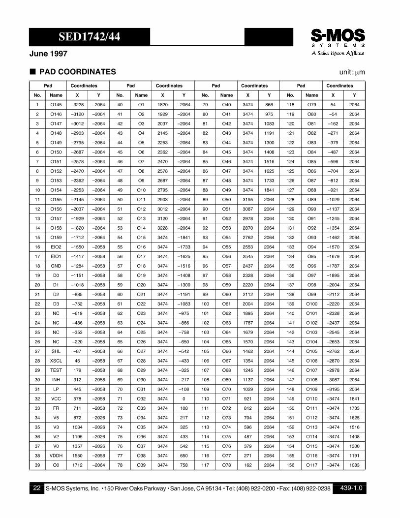
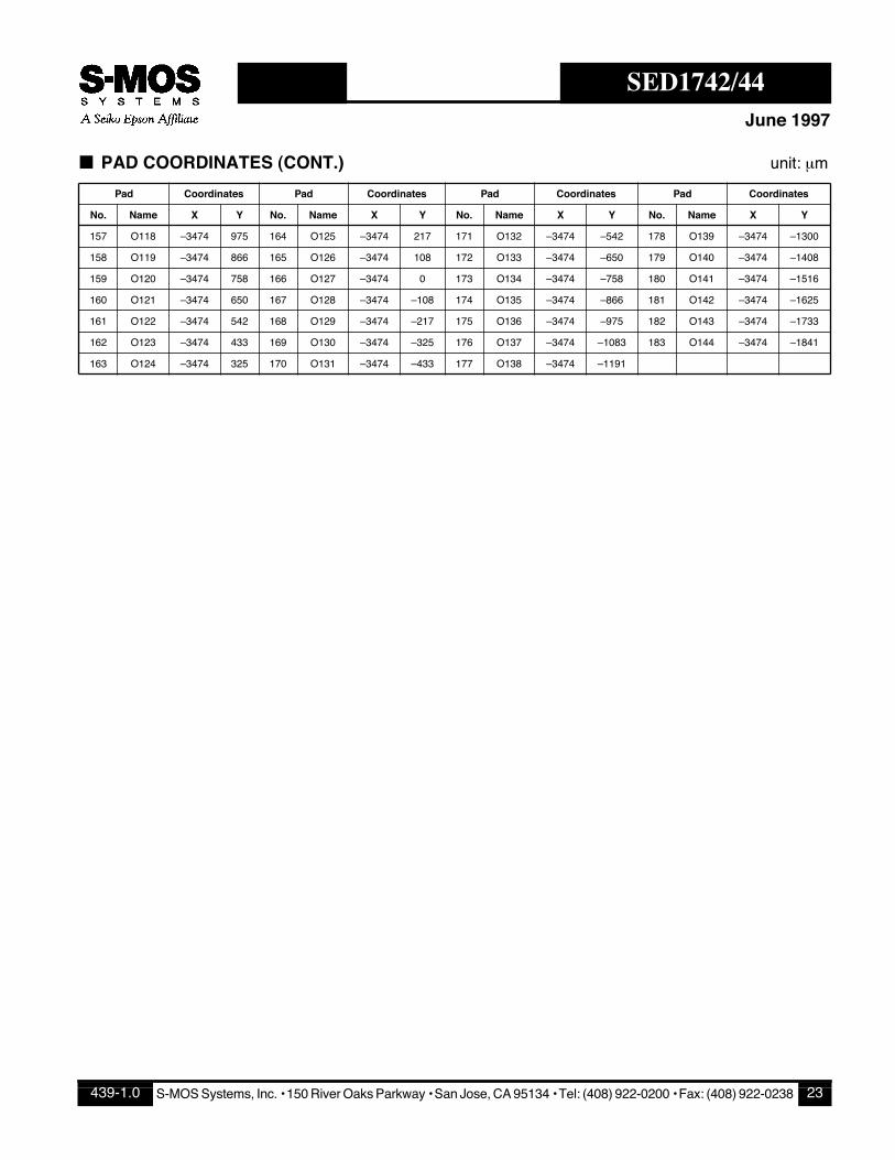
■ PAD COORDINATES unit: mm
Pad Coordinates Pad Coordinates Pad Coordinates Pad Coordinates
No. Name X Y No. Name X Y No. Name X Y No. Name X Y
1 O145 Ð3228 Ð2064 40 O1 1820 Ð2064 79 O40 3474 866 118 O79 54 2064
2 O146 Ð3120 Ð2064 41 O2 1929 Ð2064 80 O41 3474 975 119 O80 Ð54 2064
3 O147 Ð3012 Ð2064 42 O3 2037 Ð2064 81 O42 3474 1083 120 O81 Ð162 2064
4 O148 Ð2903 Ð2064 43 O4 2145 Ð2064 82 O43 3474 1191 121 O82 Ð271 2064
5 O149 Ð2795 Ð2064 44 O5 2253 Ð2064 83 O44 3474 1300 122 O83 Ð379 2064
6 O150 Ð2687 Ð2064 45 O6 2362 Ð2064 84 O45 3474 1408 123 O84 Ð487 2064
7 O151 Ð2578 Ð2064 46 O7 2470 Ð2064 85 O46 3474 1516 124 O85 Ð596 2064
8 O152 Ð2470 Ð2064 47 O8 2578 Ð2064 86 O47 3474 1625 125 O86 Ð704 2064
9 O153 Ð2362 Ð2064 48 O9 2687 Ð2064 87 O48 3474 1733 126 O87 Ð812 2064
10 O154 Ð2253 Ð2064 49 O10 2795 Ð2064 88 O49 3474 1841 127 O88 Ð921 2064
11 O155 Ð2145 Ð2064 50 O11 2903 Ð2064 89 O50 3195 2064 128 O89 Ð1029 2064
12 O156 Ð2037 Ð2064 51 O12 3012 Ð2064 90 O51 3087 2064 129 O90 Ð1137 2064
13 O157 Ð1929 Ð2064 52 O13 3120 Ð2064 91 O52 2978 2064 130 O91 Ð1245 2064
14 O158 Ð1820 Ð2064 53 O14 3228 Ð2064 92 O53 2870 2064 131 O92 Ð1354 2064
15 O159 Ð1712 Ð2064 54 O15 3474 Ð1841 93 O54 2762 2064 132 O93 Ð1462 2064
16 EIO2 Ð1550 Ð2058 55 O16 3474 Ð1733 94 O55 2553 2064 133 O94 Ð1570 2064
17 EIO1 Ð1417 Ð2058 56 O17 3474 Ð1625 95 O56 2545 2064 134 O95 Ð1679 2064
18 GND Ð1284 Ð2058 57 O18 3474 Ð1516 96 O57 2437 2064 135 O96 Ð1787 2064
19 D0 Ð1151 Ð2058 58 O19 3474 Ð1408 97 O58 2328 2064 136 O97 Ð1895 2064
20 D1 Ð1018 Ð2058 59 O20 3474 Ð1300 98 O59 2220 2064 137 O98 Ð2004 2064
21 D2 Ð885 Ð2058 60 O21 3474 Ð1191 99 O60 2112 2064 138 O99 Ð2112 2064
22 D3 Ð752 Ð2058 61 O22 3474 Ð1083 100 O61 2004 2064 139 O100 Ð2220 2064
23 NC Ð619 Ð2058 62 O23 3474 Ð975 101 O62 1895 2064 140 O101 Ð2328 2064
24 NC Ð486 Ð2058 63 O24 3474 Ð866 102 O63 1787 2064 141 O102 Ð2437 2064
25 NC Ð353 Ð2058 64 O25 3474 Ð758 103 O64 1679 2064 142 O103 Ð2545 2064
26 NC Ð220 Ð2058 65 O26 3474 Ð650 104 O65 1570 2064 143 O104 Ð2653 2064
27 SHL Ð87 Ð2058 66 O27 3474 Ð542 105 O66 1462 2064 144 O105 Ð2762 2064
28 XSCL 46 Ð2058 67 O28 3474 Ð433 106 O67 1354 2064 145 O106 Ð2870 2064
29 TEST 179 Ð2058 68 O29 3474 Ð325 107 O68 1245 2064 146 O107 Ð2978 2064
30 INH 312 Ð2058 69 O30 3474 Ð217 108 O69 1137 2064 147 O108 Ð3087 2064
31 LP 445 Ð2058 70 O31 3474 Ð108 109 O70 1029 2064 148 O109 Ð3195 2064
32 VCC 578 Ð2058 71 O32 3474 0 110 O71 921 2064 149 O110 Ð3474 1841
33 FR 711 Ð2058 72 O33 3474 108 111 O72 812 2064 150 O111 Ð3474 1733
34 V5 872 Ð2026 73 O34 3474 217 112 O73 704 2064 151 O112 Ð3474 1625
35 V3 1034 Ð2026 74 O35 3474 325 113 O74 596 2064 152 O113 Ð3474 1516
36 V2 1195 Ð2026 75 O36 3474 433 114 O75 487 2064 153 O114 Ð3474 1408
37 V0 1357 Ð2026 76 O37 3474 542 115 O76 379 2064 154 O115 Ð3474 1300
38 VDDH 1550 Ð2058 77 O38 3474 650 116 O77 271 2064 155 O116 Ð3474 1191
39 O0 1712 Ð2064 78 O39 3474 758 117 O78 162 2064 156 O117 Ð3474 1083
S-MOS Systems, Inc. ¥ 150 River Oaks Parkway ¥ San Jose, CA 95134 ¥ Tel: (408) 922-0200 ¥ Fax: (408) 922-0238439-1.0 19
SED1742/44June 1997
Pad Coordinates Pad Coordinates Pad Coordinates Pad Coordinates
No. Name X Y No. Name X Y No. Name X Y No. Name X Y
157 O118 Ð3474 975 164 O125 Ð3474 217 171 O132 Ð3474 Ð542 178 O139 Ð3474 Ð1300
158 O119 Ð3474 866 165 O126 Ð3474 108 172 O133 Ð3474 Ð650 179 O140 Ð3474 Ð1408
159 O120 Ð3474 758 166 O127 Ð3474 0 173 O134 Ð3474 Ð758 180 O141 Ð3474 Ð1516
160 O121 Ð3474 650 167 O128 Ð3474 Ð108 174 O135 Ð3474 Ð866 181 O142 Ð3474 Ð1625
161 O122 Ð3474 542 168 O129 Ð3474 Ð217 175 O136 Ð3474 Ð975 182 O143 Ð3474 Ð1733
162 O123 Ð3474 433 169 O130 Ð3474 Ð325 176 O137 Ð3474 Ð1083 183 O144 Ð3474 Ð1841
163 O124 Ð3474 325 170 O131 Ð3474 Ð433 177 O138 Ð3474 Ð1191
S-MOS Systems, Inc. ¥ 150 River Oaks Parkway ¥ San Jose, CA 95134 ¥ Tel: (408) 922-0200 ¥ Fax: (408) 922-0238 439-1.020
SED1742/44June 1997
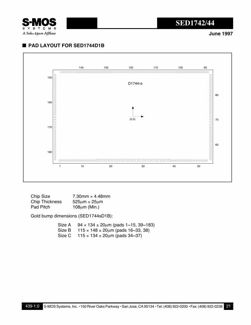
■ PAD LAYOUT FOR SED1744D1B
Chip Size 7.30mm ´ 4.48mmChip Thickness 525mm ± 25mmPad Pitch 108mm (Min.)
Gold bump dimensions (SED1744sD1B):
Size A 94 ´ 134 ± 20mm (pads 1~15, 39~183)Size B 115 ´ 148 ± 20mm (pads 16~33, 38)Size C 115 ´ 134 ± 20mm (pads 34~37)
1 10 20 30 40 50
60
70
80
90100110120130140
150
160
170
180
D17441B
(0,0)
S-MOS Systems, Inc. ¥ 150 River Oaks Parkway ¥ San Jose, CA 95134 ¥ Tel: (408) 922-0200 ¥ Fax: (408) 922-0238439-1.0 21
SED1742/44June 1997
■ PAD COORDINATES unit: mm
Pad Coordinates Pad Coordinates Pad Coordinates Pad Coordinates
No. Name X Y No. Name X Y No. Name X Y No. Name X Y
1 O145 Ð3228 Ð2064 40 O1 1820 Ð2064 79 O40 3474 866 118 O79 54 2064
2 O146 Ð3120 Ð2064 41 O2 1929 Ð2064 80 O41 3474 975 119 O80 Ð54 2064
3 O147 Ð3012 Ð2064 42 O3 2037 Ð2064 81 O42 3474 1083 120 O81 Ð162 2064
4 O148 Ð2903 Ð2064 43 O4 2145 Ð2064 82 O43 3474 1191 121 O82 Ð271 2064
5 O149 Ð2795 Ð2064 44 O5 2253 Ð2064 83 O44 3474 1300 122 O83 Ð379 2064
6 O150 Ð2687 Ð2064 45 O6 2362 Ð2064 84 O45 3474 1408 123 O84 Ð487 2064
7 O151 Ð2578 Ð2064 46 O7 2470 Ð2064 85 O46 3474 1516 124 O85 Ð596 2064
8 O152 Ð2470 Ð2064 47 O8 2578 Ð2064 86 O47 3474 1625 125 O86 Ð704 2064
9 O153 Ð2362 Ð2064 48 O9 2687 Ð2064 87 O48 3474 1733 126 O87 Ð812 2064
10 O154 Ð2253 Ð2064 49 O10 2795 Ð2064 88 O49 3474 1841 127 O88 Ð921 2064
11 O155 Ð2145 Ð2064 50 O11 2903 Ð2064 89 O50 3195 2064 128 O89 Ð1029 2064
12 O156 Ð2037 Ð2064 51 O12 3012 Ð2064 90 O51 3087 2064 129 O90 Ð1137 2064
13 O157 Ð1929 Ð2064 52 O13 3120 Ð2064 91 O52 2978 2064 130 O91 Ð1245 2064
14 O158 Ð1820 Ð2064 53 O14 3228 Ð2064 92 O53 2870 2064 131 O92 Ð1354 2064
15 O159 Ð1712 Ð2064 54 O15 3474 Ð1841 93 O54 2762 2064 132 O93 Ð1462 2064
16 EIO2 Ð1550 Ð2058 55 O16 3474 Ð1733 94 O55 2553 2064 133 O94 Ð1570 2064
17 EIO1 Ð1417 Ð2058 56 O17 3474 Ð1625 95 O56 2545 2064 134 O95 Ð1679 2064
18 GND Ð1284 Ð2058 57 O18 3474 Ð1516 96 O57 2437 2064 135 O96 Ð1787 2064
19 D0 Ð1151 Ð2058 58 O19 3474 Ð1408 97 O58 2328 2064 136 O97 Ð1895 2064
20 D1 Ð1018 Ð2058 59 O20 3474 Ð1300 98 O59 2220 2064 137 O98 Ð2004 2064
21 D2 Ð885 Ð2058 60 O21 3474 Ð1191 99 O60 2112 2064 138 O99 Ð2112 2064
22 D3 Ð752 Ð2058 61 O22 3474 Ð1083 100 O61 2004 2064 139 O100 Ð2220 2064
23 NC Ð619 Ð2058 62 O23 3474 Ð975 101 O62 1895 2064 140 O101 Ð2328 2064
24 NC Ð486 Ð2058 63 O24 3474 Ð866 102 O63 1787 2064 141 O102 Ð2437 2064
25 NC Ð353 Ð2058 64 O25 3474 Ð758 103 O64 1679 2064 142 O103 Ð2545 2064
26 NC Ð220 Ð2058 65 O26 3474 Ð650 104 O65 1570 2064 143 O104 Ð2653 2064
27 SHL Ð87 Ð2058 66 O27 3474 Ð542 105 O66 1462 2064 144 O105 Ð2762 2064
28 XSCL 46 Ð2058 67 O28 3474 Ð433 106 O67 1354 2064 145 O106 Ð2870 2064
29 TEST 179 Ð2058 68 O29 3474 Ð325 107 O68 1245 2064 146 O107 Ð2978 2064
30 INH 312 Ð2058 69 O30 3474 Ð217 108 O69 1137 2064 147 O108 Ð3087 2064
31 LP 445 Ð2058 70 O31 3474 Ð108 109 O70 1029 2064 148 O109 Ð3195 2064
32 VCC 578 Ð2058 71 O32 3474 0 110 O71 921 2064 149 O110 Ð3474 1841
33 FR 711 Ð2058 72 O33 3474 108 111 O72 812 2064 150 O111 Ð3474 1733
34 V5 872 Ð2026 73 O34 3474 217 112 O73 704 2064 151 O112 Ð3474 1625
35 V3 1034 Ð2026 74 O35 3474 325 113 O74 596 2064 152 O113 Ð3474 1516
36 V2 1195 Ð2026 75 O36 3474 433 114 O75 487 2064 153 O114 Ð3474 1408
37 V0 1357 Ð2026 76 O37 3474 542 115 O76 379 2064 154 O115 Ð3474 1300
38 VDDH 1550 Ð2058 77 O38 3474 650 116 O77 271 2064 155 O116 Ð3474 1191
39 O0 1712 Ð2064 78 O39 3474 758 117 O78 162 2064 156 O117 Ð3474 1083
S-MOS Systems, Inc. ¥ 150 River Oaks Parkway ¥ San Jose, CA 95134 ¥ Tel: (408) 922-0200 ¥ Fax: (408) 922-0238 439-1.022
SED1742/44June 1997
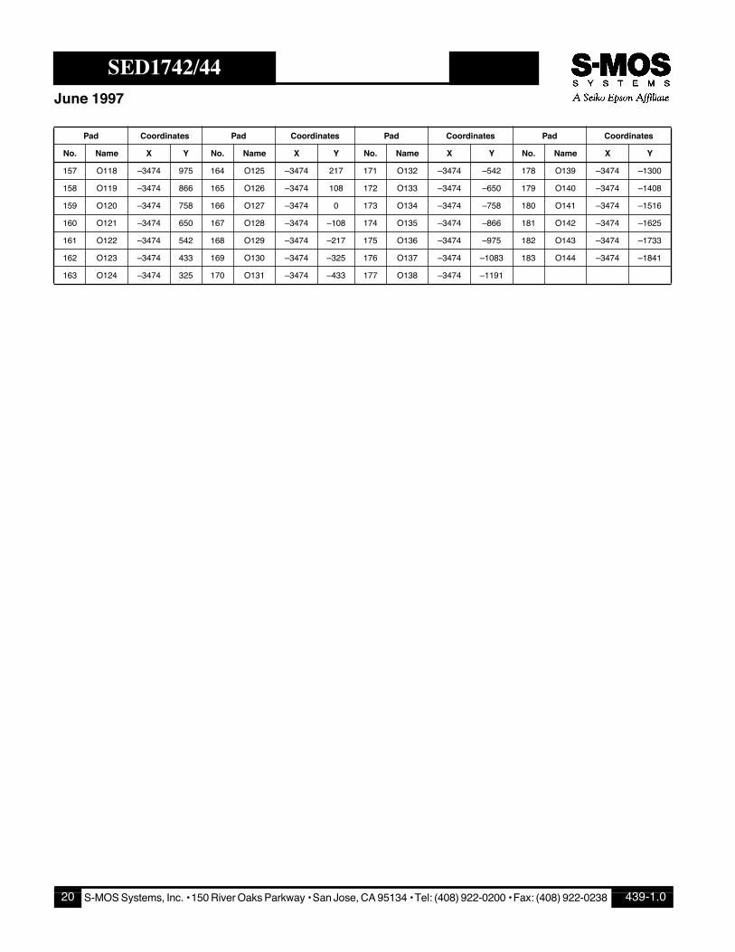
■ PAD COORDINATES (CONT.) unit: mm
Pad Coordinates Pad Coordinates Pad Coordinates Pad Coordinates
No. Name X Y No. Name X Y No. Name X Y No. Name X Y
157 O118 Ð3474 975 164 O125 Ð3474 217 171 O132 Ð3474 Ð542 178 O139 Ð3474 Ð1300
158 O119 Ð3474 866 165 O126 Ð3474 108 172 O133 Ð3474 Ð650 179 O140 Ð3474 Ð1408
159 O120 Ð3474 758 166 O127 Ð3474 0 173 O134 Ð3474 Ð758 180 O141 Ð3474 Ð1516
160 O121 Ð3474 650 167 O128 Ð3474 Ð108 174 O135 Ð3474 Ð866 181 O142 Ð3474 Ð1625
161 O122 Ð3474 542 168 O129 Ð3474 Ð217 175 O136 Ð3474 Ð975 182 O143 Ð3474 Ð1733
162 O123 Ð3474 433 169 O130 Ð3474 Ð325 176 O137 Ð3474 Ð1083 183 O144 Ð3474 Ð1841
163 O124 Ð3474 325 170 O131 Ð3474 Ð433 177 O138 Ð3474 Ð1191
S-MOS Systems, Inc. ¥ 150 River Oaks Parkway ¥ San Jose, CA 95134 ¥ Tel: (408) 922-0200 ¥ Fax: (408) 922-0238439-1.0 23
SED1742/44June 1997
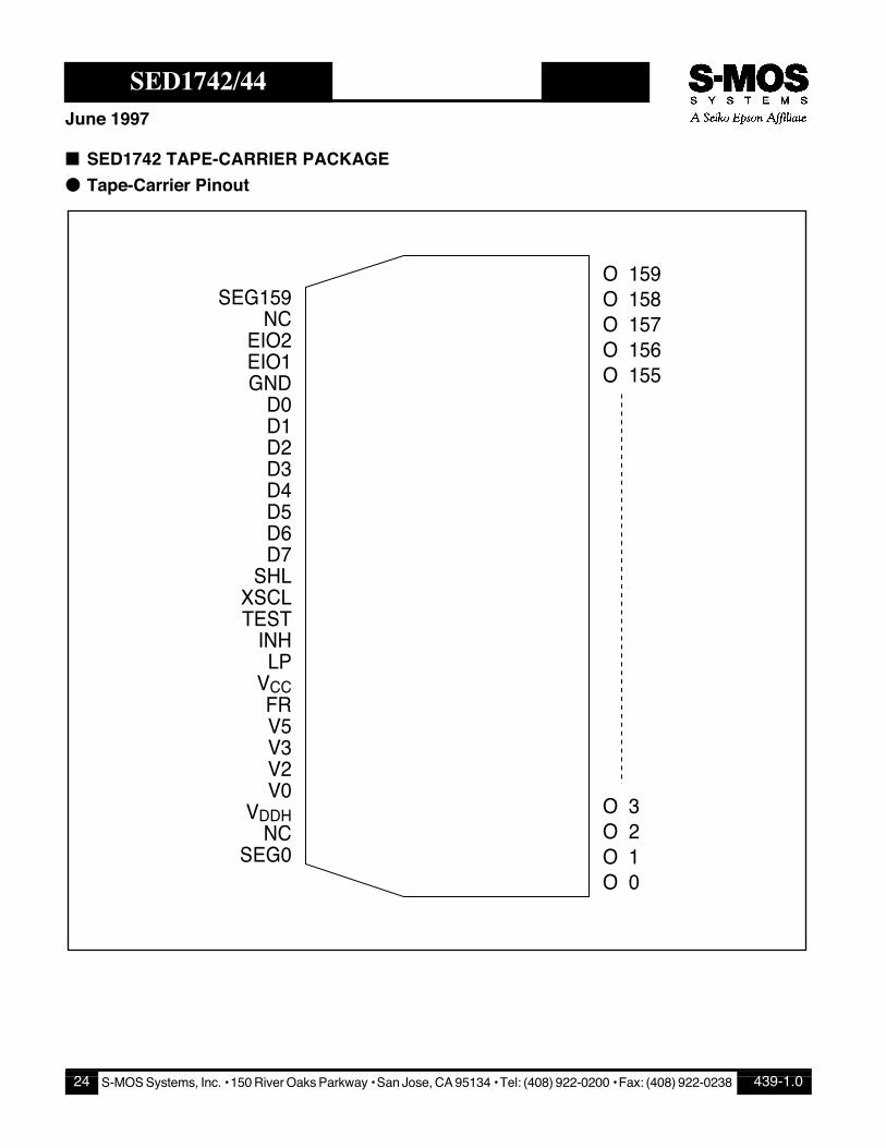
■ SED1742 TAPE-CARRIER PACKAGE
● Tape-Carrier Pinout
O 159O 158O 157O 156O 155
O 3O 2O 1O 0
SEG159NC
EIO2EIO1GND
D0D1D2D3D4D5D6D7
SHLXSCLTEST
INHLP
VCCFRV5V3V2V0
VDDHNC
SEG0
S-MOS Systems, Inc. ¥ 150 River Oaks Parkway ¥ San Jose, CA 95134 ¥ Tel: (408) 922-0200 ¥ Fax: (408) 922-0238 439-1.024
SED1742/44June 1997
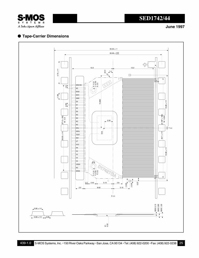
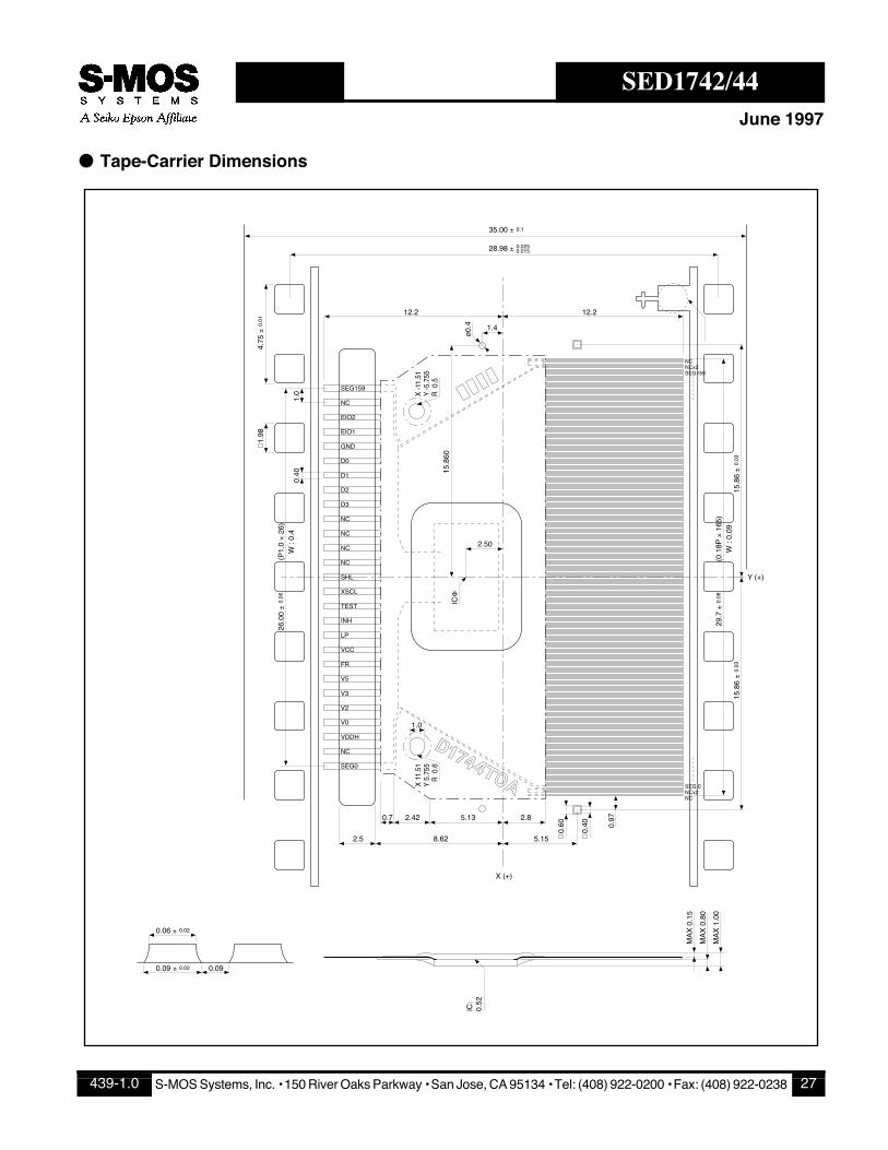
● Tape-Carrier Dimensions
0.09 ± 0.02
0.06 ± 0.02
0.09
2.5
2.42
2.50
ICF
1.4
12.2 12.2
28.98 ± 0.025
35.00 ± 0.1
¿0.
4
0.60
2.85.130.7
0.40
1.0
1.98
4.75
± 0
.01
15.8
60
1.0
X 1
1.51
Y 5
.755
R 0
.6
X -1
1.51
Y -5
.755
R 0
.5
5.15
15.8
6 ±
0.03
26.0
0 ±
0.06
(P1.
0 ´
26)
W :
0.4
29.7
± 0
.08
(0.1
8P ´
165
)W
: 0.
0915
.86 ±
0.03
8.62
IC:
0.52
MA
X 0
.15
MA
X 0
.80
MA
X 1
.00
0.40 0.
97�
0.015
Y (+)
X (+)
NCNCx2SEG159
SEG 0NCx2NC
SEG159
NC
EIO2
EIO1
GND
D0
D1
D2
D3
NC
NC
NC
NC
SHL
XSCL
TEST
INH
LP
VCC
FR
V5
V3
V2
V0
VDDH
NC
SEG0
S-MOS Systems, Inc. ¥ 150 River Oaks Parkway ¥ San Jose, CA 95134 ¥ Tel: (408) 922-0200 ¥ Fax: (408) 922-0238439-1.0 25
SED1742/44June 1997
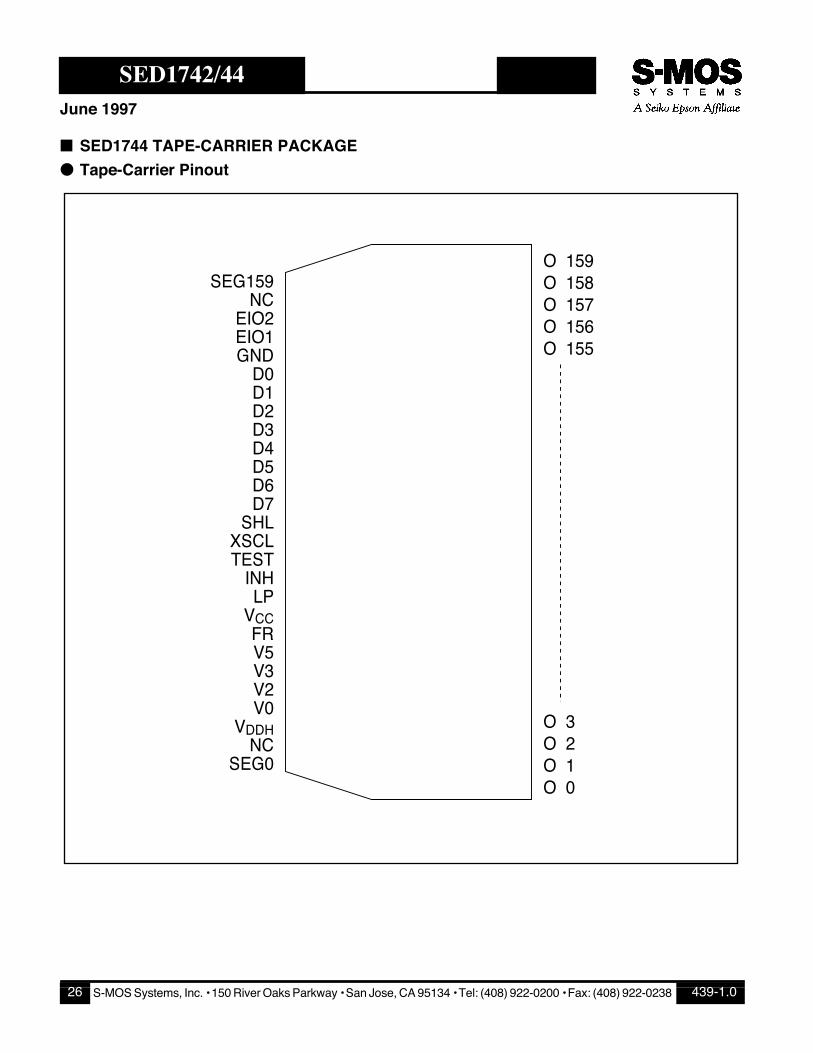
■ SED1744 TAPE-CARRIER PACKAGE
● Tape-Carrier Pinout
O 159O 158O 157O 156O 155
O 3O 2O 1O 0
SEG159NC
EIO2EIO1GND
D0D1D2D3D4D5D6D7
SHLXSCLTEST
INHLP
VCCFRV5V3V2V0
VDDHNC
SEG0
S-MOS Systems, Inc. ¥ 150 River Oaks Parkway ¥ San Jose, CA 95134 ¥ Tel: (408) 922-0200 ¥ Fax: (408) 922-0238 439-1.026
SED1742/44June 1997
● Tape-Carrier Dimensions
0.09 ± 0.02
0.06 ± 0.02
0.09
2.5
2.42
2.50
ICF
1.4
12.2 12.2
28.98 ± 0.025
35.00 ± 0.1
¿0.
4
0.60
2.85.130.7
0.40
1.0
1.98
4.75
± 0
.01
15.8
60
1.0
X 1
1.51
Y 5
.755
R 0
.6
X -1
1.51
Y -5
.755
R 0
.5
5.15
15.8
6 ±
0.03
26.0
0 ±
0.06
(P1.
0 ´
26)
W :
0.4
29.7
± 0
.08
(0.1
8P ´
165
)W
: 0.
0915
.86 ±
0.03
8.62
IC:
0.52
MA
X 0
.15
MA
X 0
.80
MA
X 1
.00
0.40 0.
97�
0.015
Y (+)
X (+)
NCNCx2SEG159
SEG 0NCx2NC
SEG159
NC
EIO2
EIO1
GND
D0
D1
D2
D3
NC
NC
NC
NC
SHL
XSCL
TEST
INH
LP
VCC
FR
V5
V3
V2
V0
VDDH
NC
SEG0
S-MOS Systems, Inc. ¥ 150 River Oaks Parkway ¥ San Jose, CA 95134 ¥ Tel: (408) 922-0200 ¥ Fax: (408) 922-0238439-1.0 27
SED1742/44June 1997
S-MOS assumes no responsibility or liability for (1) any errors or inaccuracies contained in theinformation herein and (2) the use of the information or a portion thereof in any application, in-cluding any claim for (a) copyright or patent infringement or (b) direct, indirect, special or conse-quential damages. There are no warranties extended or granted by this document. Theinformation herein is subject to change without notice from S-MOS.
June 1997 © Copyright 1997 S-MOS Systems, Inc. Printed in U.S.A. RDG.
S-MOS Systems, Inc. ¥ 150 River Oaks Parkway ¥ San28
Jose, CA 95134 ¥ Tel: (408) 922-0200 ¥ Fax: (408) 922-0238 439-1.0


![F3JR MB R20 1211[31731]ncandelier.free.fr/asus/ASUS_F3JR_R20.pdfH_D#50 H_TMS H_TDO H_TCK H_TRST# H_PREQ# +VCCP +VCCP +VCCP +VCCP GND GND GND GND GND GND GND TPC26T 1 T1 R8 1 2 56Ohm](https://img.pdfslide.us/doc/110x75/5faf0ab01979a324157ec2b6/f3jr-mb-r20-121131731-hd50-htms-htdo-htck-htrst-hpreq-vccp-vccp-vccp.jpg)