Embed Size (px)
Citation preview
Outline
• Introduction
• Theory and concept of junction
• Technology of junction
• Types of junction in devices
Junction – Part 1
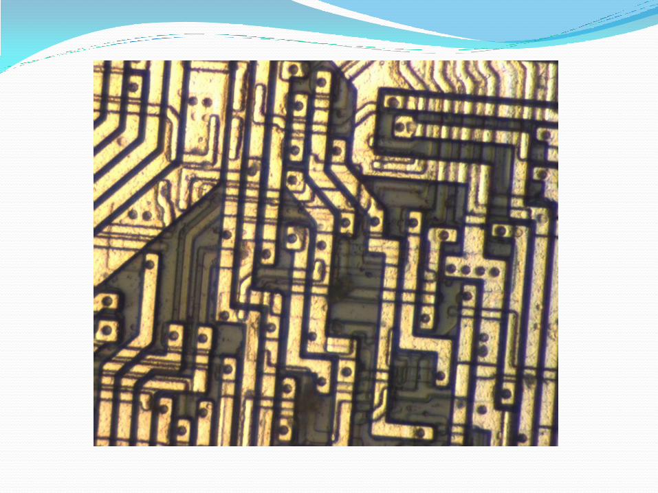

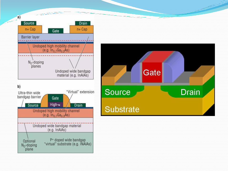
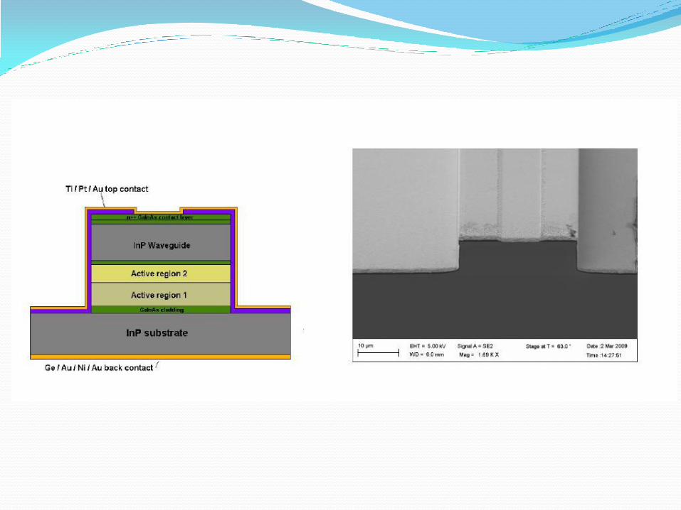
Example: Cross section
Introduction • What is a junction?
A boundary region between domains with dissimilar
electronic characteristics. Examples: p-n junction in
diodes and transistors, heterojunction between
different semiconductors, insulator-metal or
insulator-semiconductor junctions, Ohmic and
Schottky metal-semiconductor junctions
• Why junctions?
A device without any junctions is a piece of material
with uniform characteristic throughout. What do you
think its electrical behavior is like? e. g. I-V curve?
what can we do with it?

Example: Cross section
How to make junctions • Put 2 dissimilar domains together: deposition, epitaxial
growth
• Induce a change in a small domain within a larger
domain. The change can be: carrier types, carrier
concentration and/or spatial profile. Alloying, diffusion,
ion implantation.
• Making junctions is almost the same as making
devices. Extensive R&D have been devoted to the
fabrication technology. Many problems have been
solved, but from time to time, still new progress,
breakthru http://www.youtube.com/watch?v=TXvhyvwttRE
What about junctions? • How does it work?
• How does a junction behave in an electrical circuit? Is it
like an R, C, L, or a vacuum diode? How do we
describe its properties? If a junction behaves like an R,
C, or L, is there any reason for us to be so interested in
them?
• How is it applied?
• Junction is the key building block of solid state
devices:
• Fundamental physics
• Material and fabrication technology
• Device design
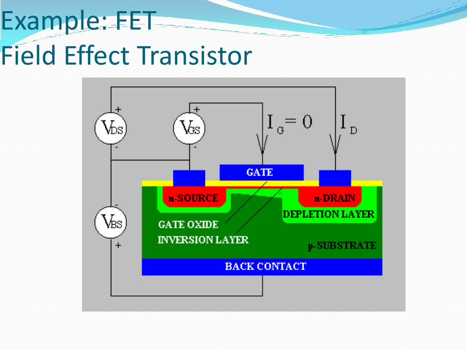
Example: FET Field Effect Transistor

Approaches to study junction • Types of junctions
• Homogenous semiconductors: same-chemical
composition semiconductors; e. g. Si p-n junction
• Heterogenous semiconductors (also called
heterojunctions): different alloys, chemical
compositions
• Semiconductor-dielectric insulator (e. g. FET)
• Semiconductor-metal: ohmic and Schottky.
• Physical junctions vs. idealized junctions: modeling
• Approximations for various regimes
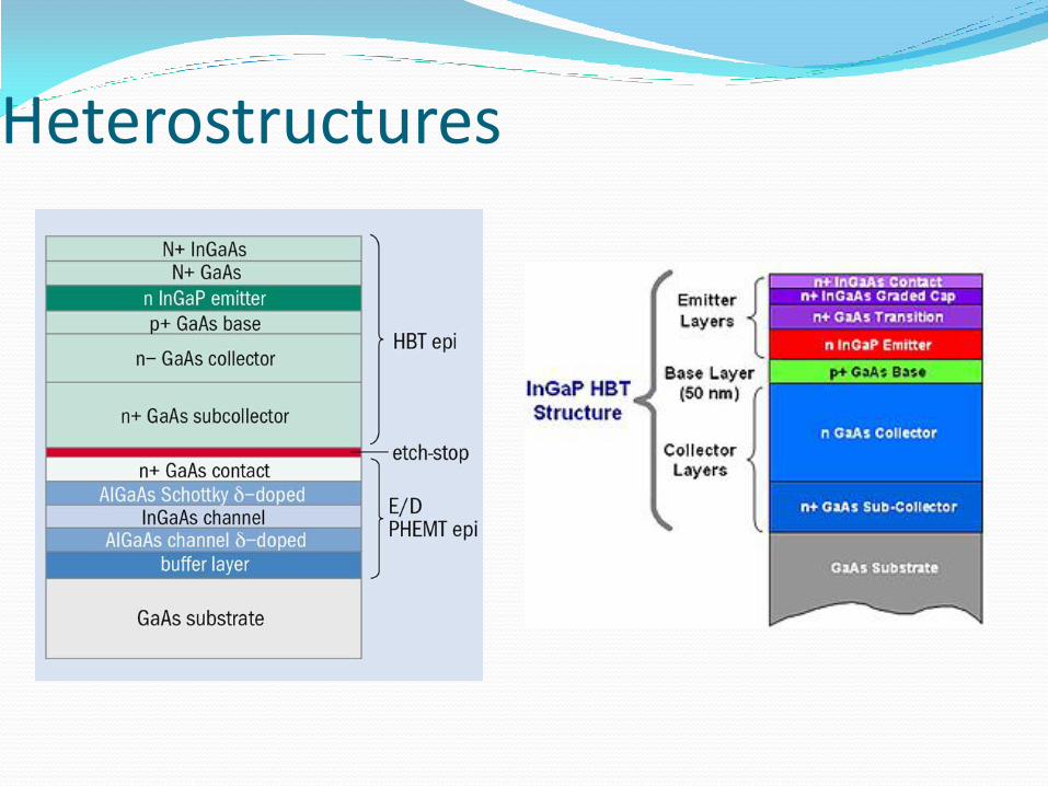
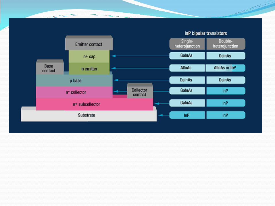
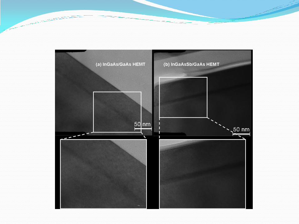
Heterostructures
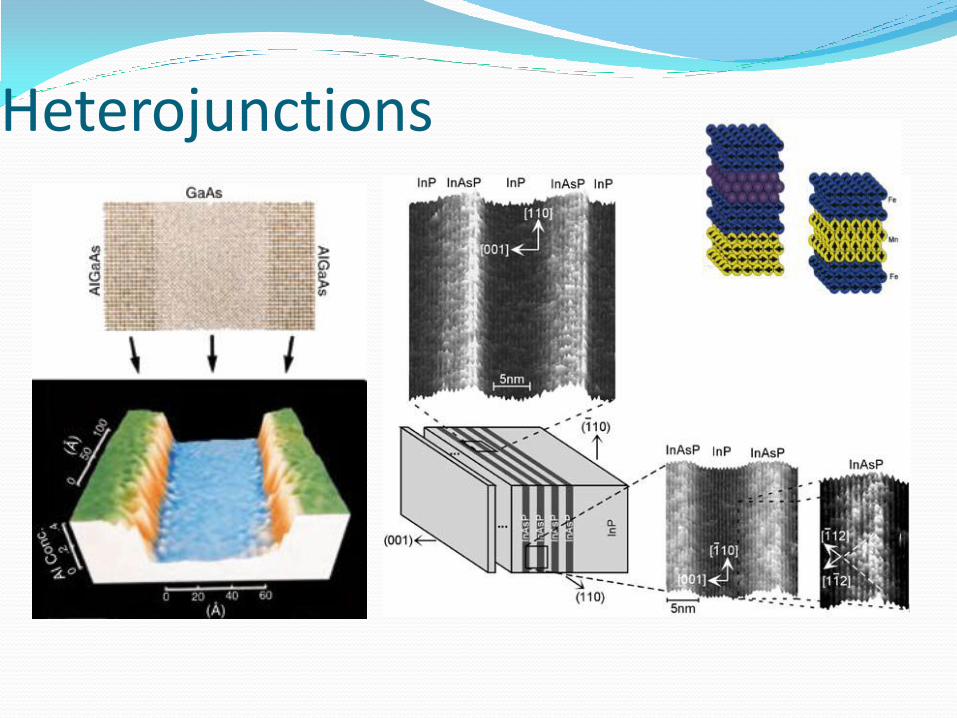
Heterojunctions

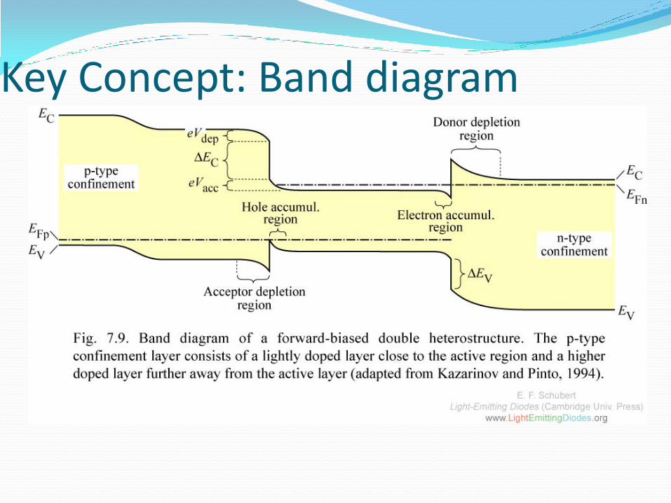
Key Concept: Band diagram
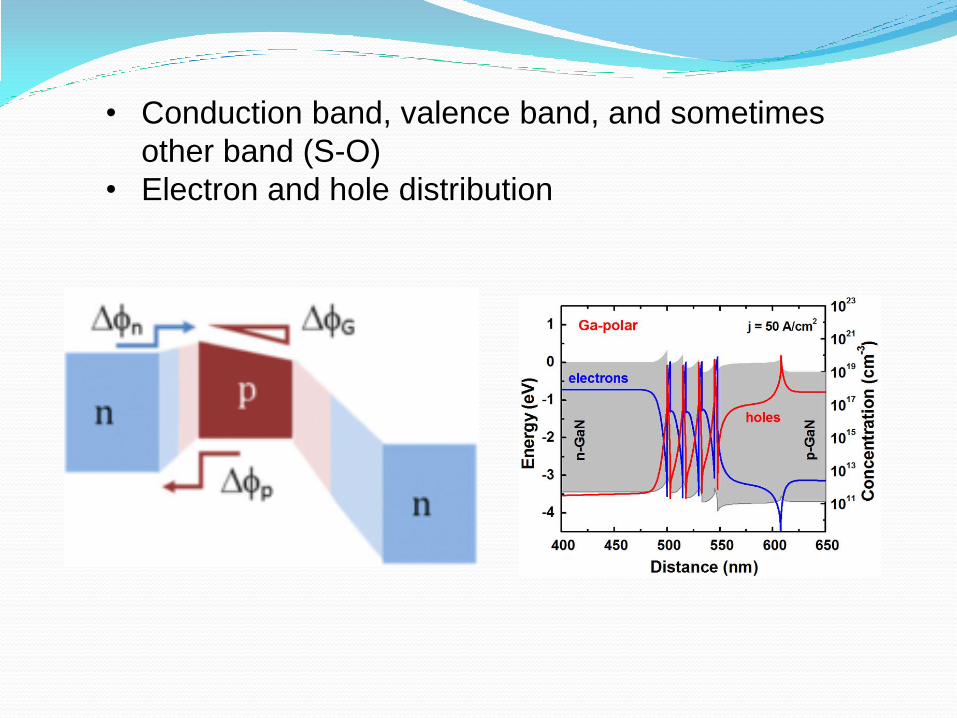
• Conduction band, valence band, and sometimes
other band (S-O)
• Electron and hole distribution
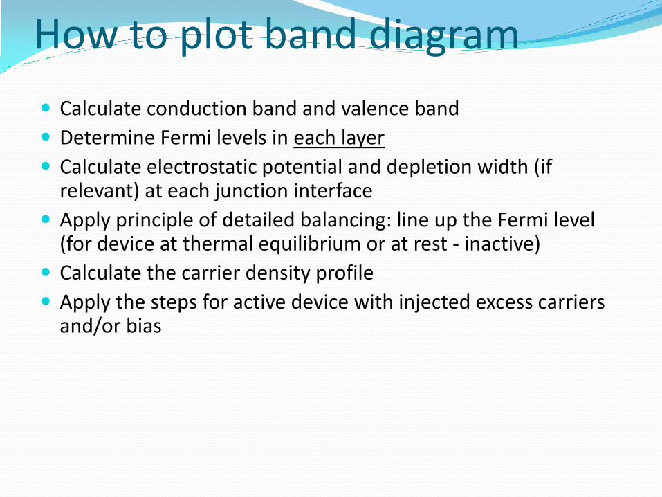
How to plot band diagram
Calculate conduction band and valence band
Determine Fermi levels in each layer
Calculate electrostatic potential and depletion width (if relevant) at each junction interface
Apply principle of detailed balancing: line up the Fermi level (for device at thermal equilibrium or at rest - inactive)
Calculate the carrier density profile
Apply the steps for active device with injected excess carriers and/or bias

Study topics in p-n junction
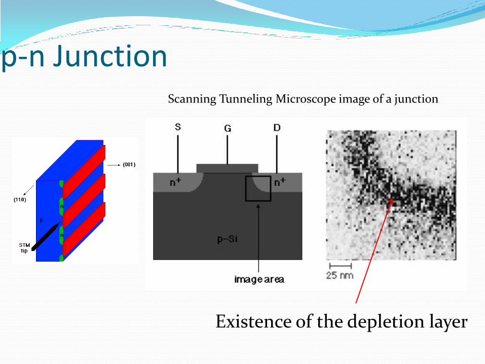
p-n Junction Scanning Tunneling Microscope image of a junction
Existence of the depletion layer
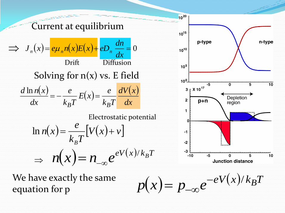
0dx
dneDxExnexJ nnn
dx
xdV
Tk
exE
Tk
e
dx
xnd
BB
ln
TkxeV Benxn/
TkxeV Bepxp/
Current at equilibrium
Diffusion Drift
Solving for n(x) vs. E field
Electrostatic potential
We have exactly the same equation for p
vxVTk
exn
B
ln
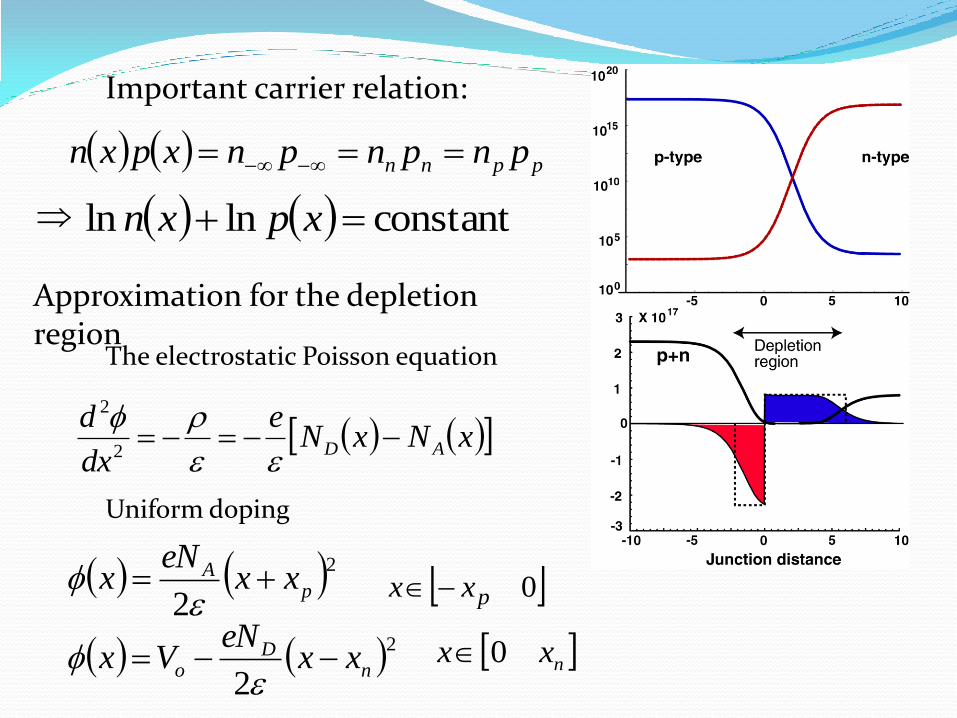
ppnn pnpnpnxpxn
constantlnln xpxn
Important carrier relation:
Approximation for the depletion region
xNxNe
dx
dAD
2
2
The electrostatic Poisson equation
Uniform doping
22
pA xx
eNx
0pxx
22
nD
o xxeN
Vx
nxx 0
22
220 p
An
Do x
eNx
eNV
22
22p
An
Do x
eNx
eNV
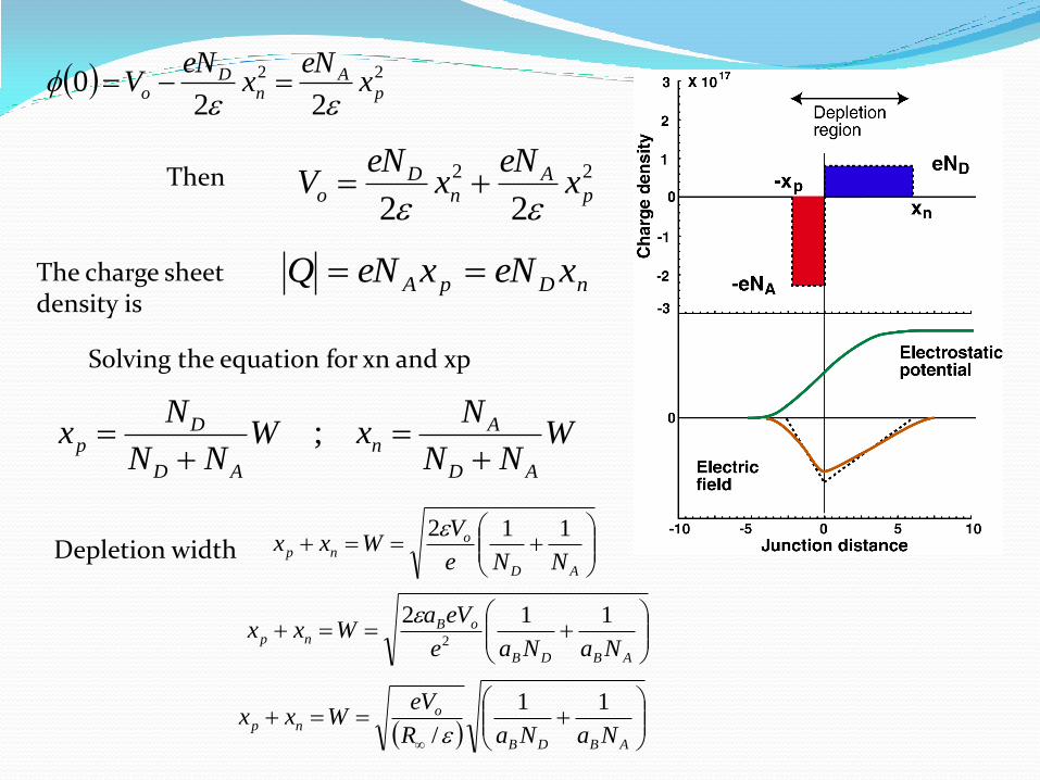
nDpA xeNxeNQ
Then
The charge sheet density is
WNN
NxW
NN
Nx
AD
An
AD
Dp
;
Solving the equation for xn and xp
AD
onp
NNe
VWxx
112Depletion width
ABDB
oBnp
NaNae
eVaWxx
1122
ABDB
onp
NaNaR
eVWxx
11
/
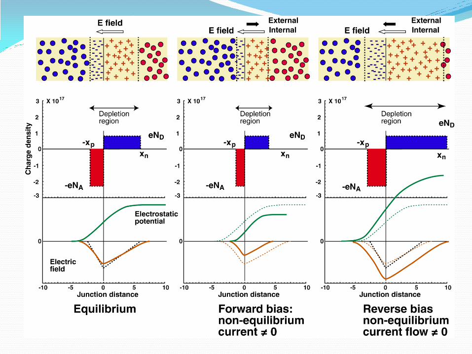
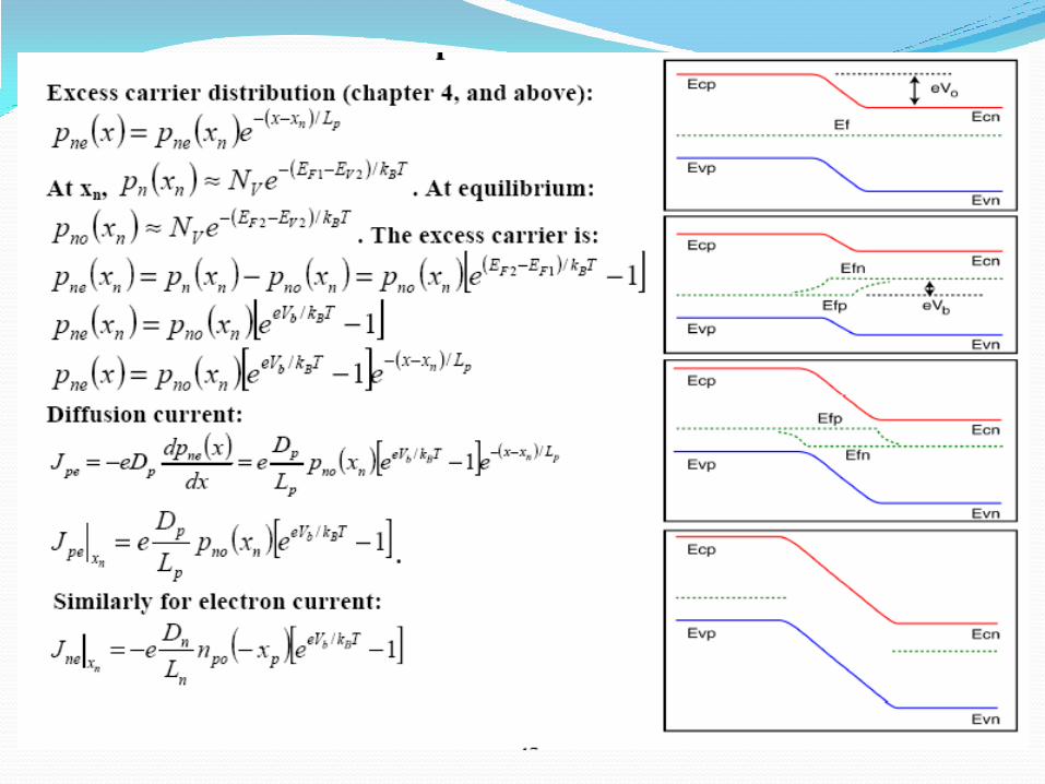
• At junctions: electron diffuses to p-side and hole diffuse to n-side. They
recombine (cancel each other out) in the middle, resulting in a carrier
depletion region
• Without carriers in the depletion region, space charge from ionized
donors and acceptors appears, resulting in electrostatic field and
potential. Net charge is still and always zero.
• The larger the depletion width, the more space charge exposed, the
higher the electrostatic field and potential.
• Vice versa, the carriers continue to diffuse and enlarge the depletion
width until the build up electrostatic field and potential are strong enough
to counter the carrier diffusion pressure: equilibrium is reached
• Carrier diffusion “potential” is negatively proportional to the depletion
width. The electrostatic potential is ~ x2. Therefore, the depletion width is
~ square root of electrostatic potential. Similarly, higher dopant density
higher electrostatic potential smaller depletion width.
• External bias reducing the internal field: smaller depletion width, higher
diffusion current; Ext. bias enhances the internal field: larger depletion
width, lower diffusion
Summary of key features

Lecture 2

A non-technical analogy
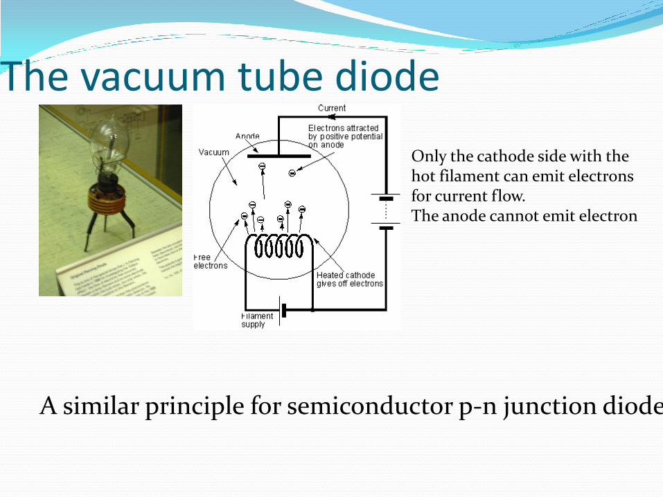
The vacuum tube diode
Only the cathode side with the hot filament can emit electrons for current flow. The anode cannot emit electron
A similar principle for semiconductor p-n junction diode
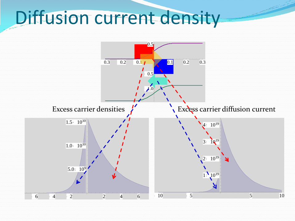
Diffusion current density
Excess carrier densities
6 4 2 2 4 6
5.0 109
1.0 1010
1.5 1010
0.3 0.2 0.1 0.1 0.2 0.3
1.0
0.5
0.5
10 5 5 10
1 1019
2 1019
3 1019
4 1019
Excess carrier diffusion current
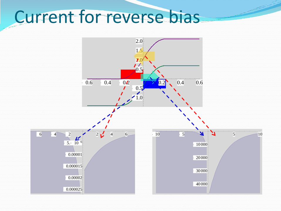
Current for reverse bias
0.6 0.4 0.2 0.2 0.4 0.6
1.0
0.5
0.5
1.0
1.5
2.0
6 4 2 2 4 6
0.000025
0.00002
0.000015
0.00001
5. 10 6
10 5 5 10
40000
30000
20000
10000
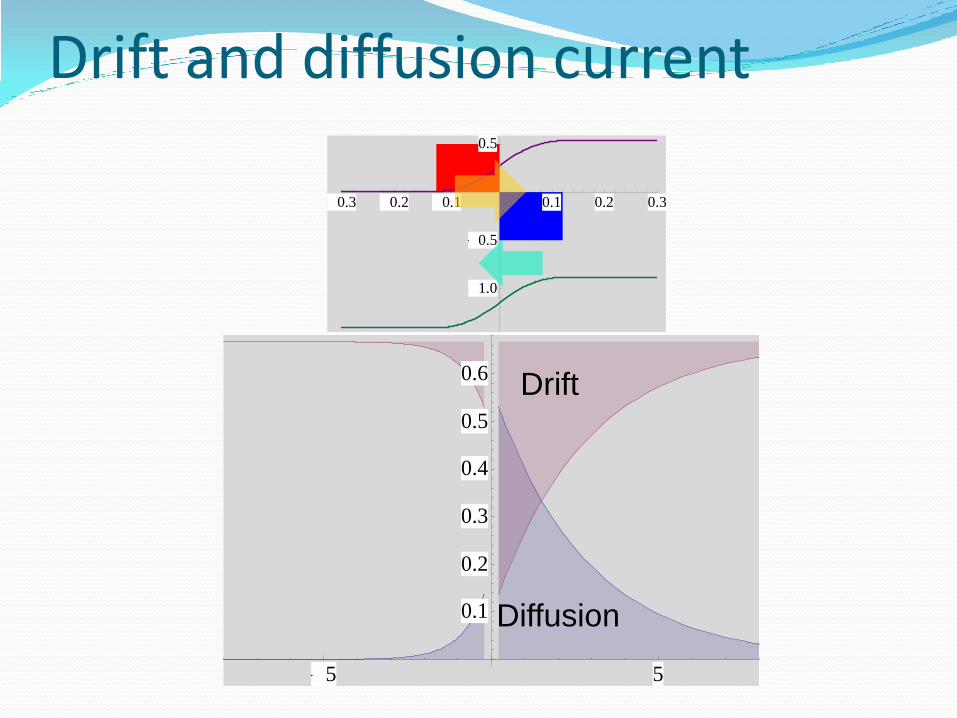
Drift and diffusion current
5 5
0.1
0.2
0.3
0.4
0.5
0.6
0.3 0.2 0.1 0.1 0.2 0.3
1.0
0.5
0.5
Diffusion
Drift
• An external electric field will disturb the equilibrium at
junctions. Carriers want to return to equilibrium. Continuous
injection (pumping) of carrier is necessary to maintain non-
equilibrium condition: current flows to maintain a steady
state
• Excess holes must diffuse to n-side and excess electrons
must diffuse to p-side. Diffusion current is much larger than
drift current across the junction. In one dimension, the
diffusion profile is ~ exponential vs. distance.
• Hole current in n-region and electron current in p-region are
called minority carrier currents.
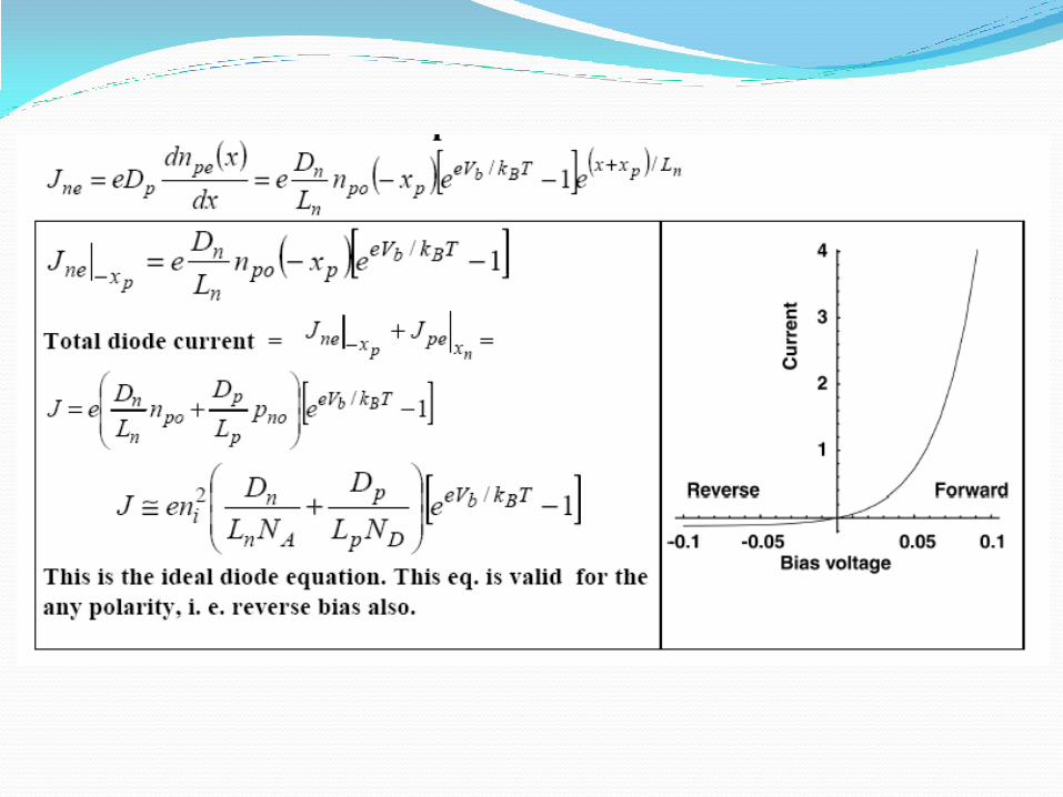
Ideal diode key features
• The diffusion current is proportional to the excess carrier
density. The excess carrier density is approximately
exponentially dependent on the difference between quasi-
Fermi levels which is the bias voltage. Therefore, forward
bias current is exponentially dependent on bias voltage.
• On reverse bias, there is no excess current (may be we
should call deficiency current!). Holes from n-region and
electrons from p-region (minority carriers) carry the current:
very small and quickly saturate.
• On forward bias, weaker internal electric field the depletion
width is reduced as the junction potential drop is reduced.
On reverse bias, the depletion width increases with larger
potential drop
Ideal diode key features (continued)
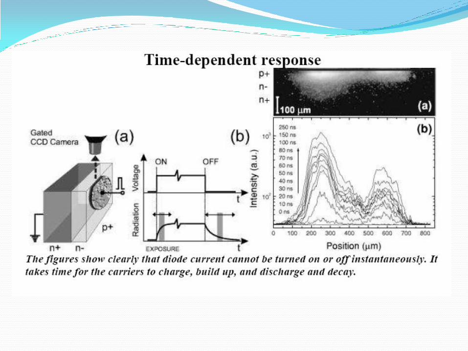
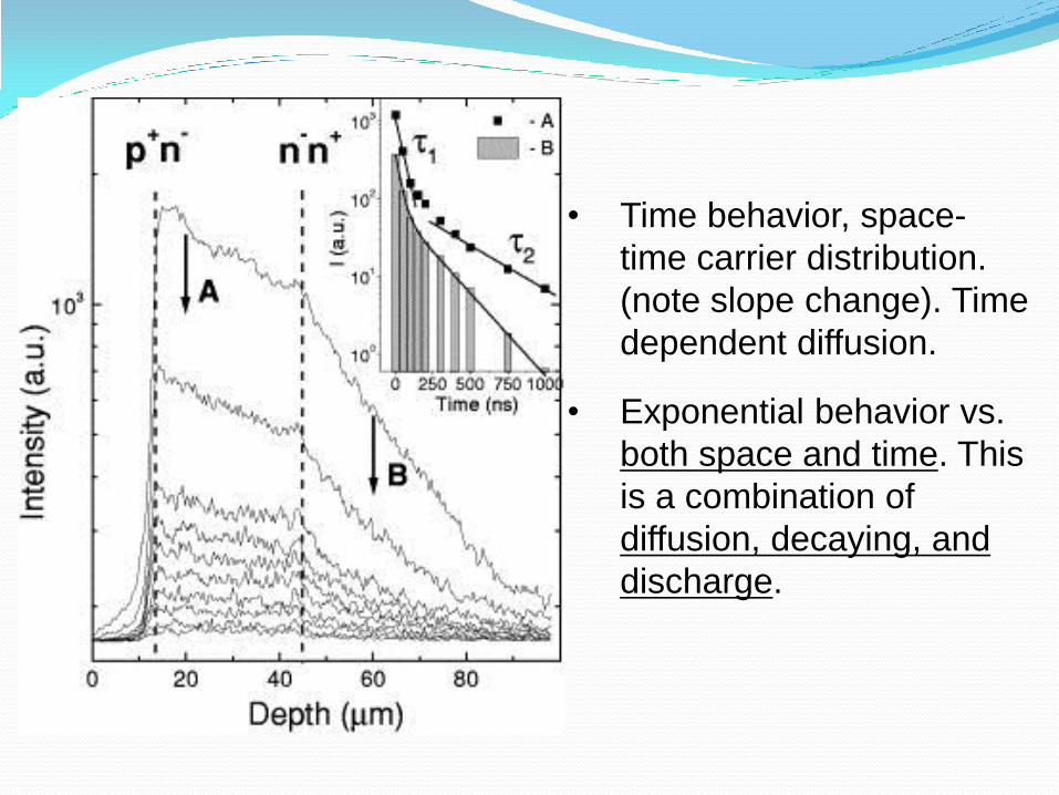
• Time behavior, space-
time carrier distribution.
(note slope change). Time
dependent diffusion.
• Exponential behavior vs.
both space and time. This
is a combination of
diffusion, decaying, and
discharge.
F
nPnD
nP
t
n 2
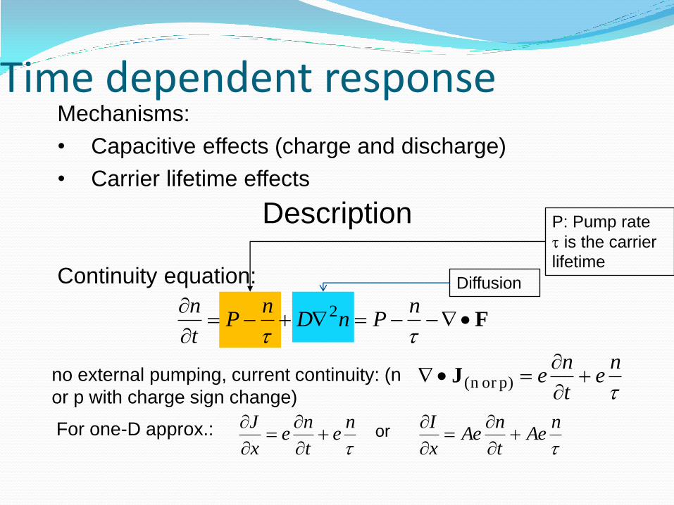
Time dependent response
p)or n (
ne
t
ne
J
ne
t
ne
x
J
nAe
t
nAe
x
I
Mechanisms:
• Capacitive effects (charge and discharge)
• Carrier lifetime effects
no external pumping, current continuity: (n
or p with charge sign change)
or
Description
Continuity equation:
P: Pump rate
is the carrier
lifetime
Diffusion
For one-D approx.:

Time dependent response (cont.)
xxdtnAedtn
tAetxI
,
1,,
txQ
t
txQtxI
,,,
Integration:
Since: txQdtn
x,,
Space
dependent
charge
Charge lifetime
(decaying term) Capacitive effect: Charge
time-dependent term due to
migration, drift or diffusion:
Time dependent response (cont.)
tQ
t
tQtInet
At x-> infinity
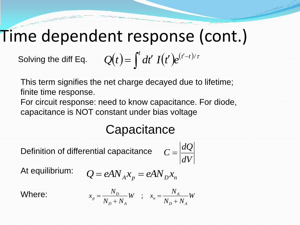
Time dependent response (cont.)
tttetItdtQ /Solving the diff Eq.
This term signifies the net charge decayed due to lifetime;
finite time response.
For circuit response: need to know capacitance. For diode,
capacitance is NOT constant under bias voltage
dV
dQC Definition of differential capacitance
nDpA xeANxeANQ At equilibrium:
WNN
NxW
NN
Nx
AD
An
AD
Dp
;Where:
Capacitance
AD
bonp
NNe
VVWxx
112
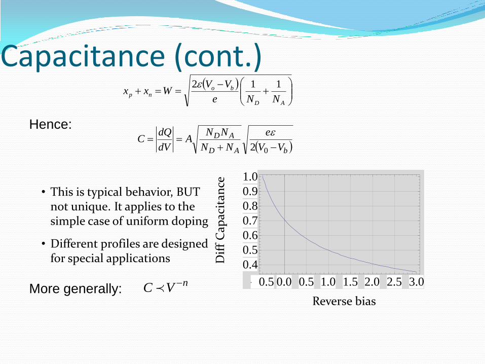
Capacitance (cont.)
Hence:
bAD
AD
VV
e
NN
NNA
dV
dQC
02
0.5 0.0 0.5 1.0 1.5 2.0 2.5 3.0
0.4
0.5
0.6
0.7
0.8
0.9
1.0
Reverse bias
Dif
f C
apac
itan
ce
• This is typical behavior, BUT not unique. It applies to the simple case of uniform doping
• Different profiles are designed for special applications
More generally: nVC
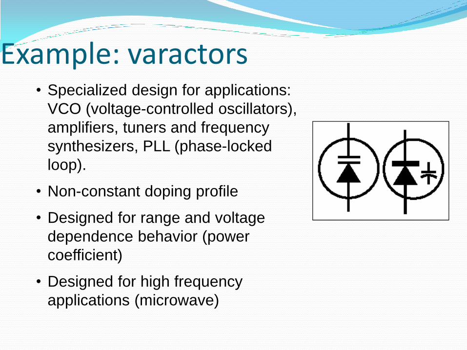
Example: varactors • Specialized design for applications:
VCO (voltage-controlled oscillators),
amplifiers, tuners and frequency
synthesizers, PLL (phase-locked
loop).
• Non-constant doping profile
• Designed for range and voltage
dependence behavior (power
coefficient)
• Designed for high frequency
applications (microwave)
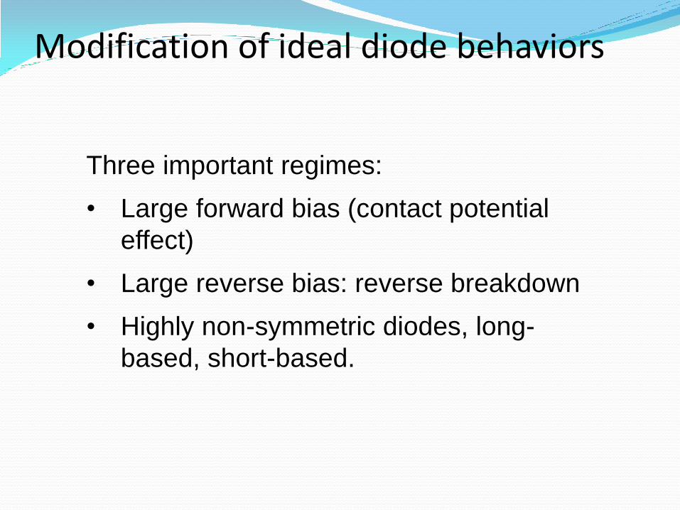
Modification of ideal diode behaviors
Three important regimes:
• Large forward bias (contact potential
effect)
• Large reverse bias: reverse breakdown
• Highly non-symmetric diodes, long-
based, short-based.
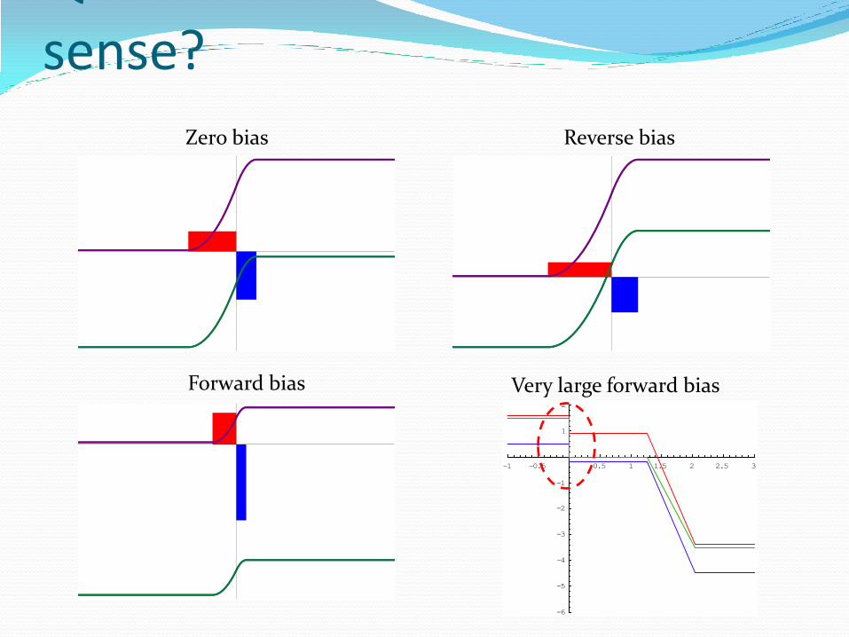
Question: Does this make sense?
Zero bias Reverse bias
Forward bias Very large forward bias
-1 -0.5 0.5 1 1.5 2 2.5 3
-6
-5
-4
-3
-2
-1
1
2
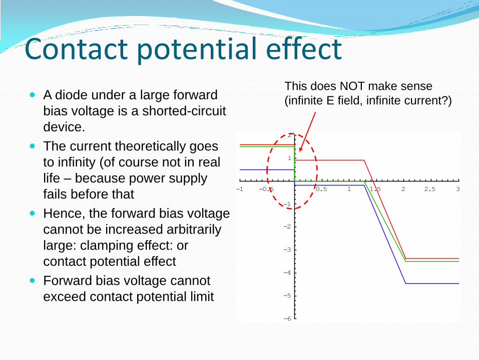
Contact potential effect A diode under a large forward
bias voltage is a shorted-circuit
device.
The current theoretically goes
to infinity (of course not in real
life – because power supply
fails before that
Hence, the forward bias voltage
cannot be increased arbitrarily
large: clamping effect: or
contact potential effect
Forward bias voltage cannot
exceed contact potential limit
-1 -0.5 0.5 1 1.5 2 2.5 3
-6
-5
-4
-3
-2
-1
1
2
This does NOT make sense
(infinite E field, infinite current?)
Large forward bias
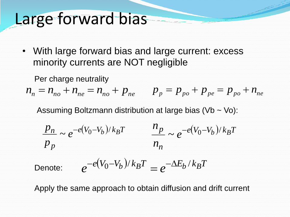
• With large forward bias and large current: excess minority currents are NOT negligible
nenonenon pnnnn nepopepop npppp Per charge neutrality
Assuming Boltzmann distribution at large bias (Vb ~ Vo):
TkVVe
p
n Bbep
p /0~ TkVVe
n
p Bben
n /0~
TkETkVVe BbBb ee//0
Denote:
Apply the same approach to obtain diffusion and drift current
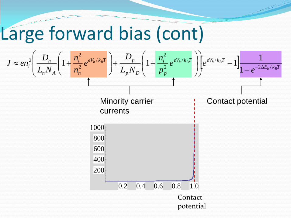
TkE
TkeVTkeV
p
i
Dp
pTkeV
n
i
An
ni
Bb
BbBbBb
eee
p
n
NL
De
n
n
NL
DenJ
/2
//
2
2/
2
22
1
1111
Large forward bias (cont)
Minority carrier
currents
Contact potential
Contact potential
0.2 0.4 0.6 0.8 1.0
200
400
600
800
1000
Large reverse bias Breakdown: Not the same as broken- although many
diodes can be damaged with large reverse breakdown current
A regime where simply the low voltage drift and diffusion current model is NOT sufficient
Involve quantum tunneling effect and high field transport effects (non classical behaviors)
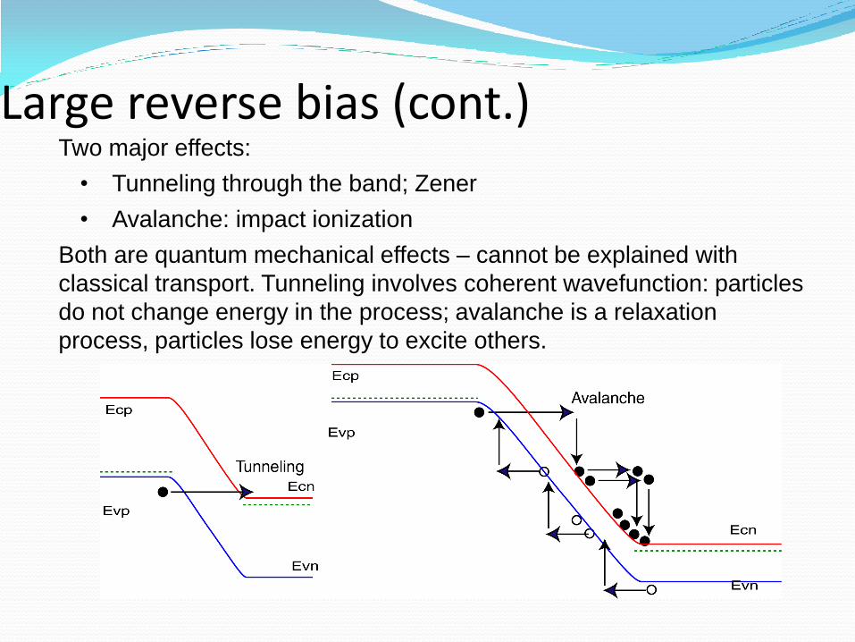
Large reverse bias (cont.) Two major effects:
• Tunneling through the band; Zener
• Avalanche: impact ionization
Both are quantum mechanical effects – cannot be explained with
classical transport. Tunneling involves coherent wavefunction: particles
do not change energy in the process; avalanche is a relaxation
process, particles lose energy to excite others.
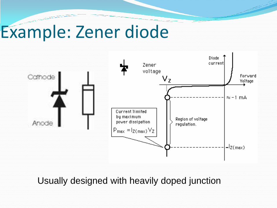
Example: Zener diode
Usually designed with heavily doped junction

Example: avalanche diode
Avalanche region is undoped
or very lightly doped (so as
not to quench carriers)
One significant application is
photodetection
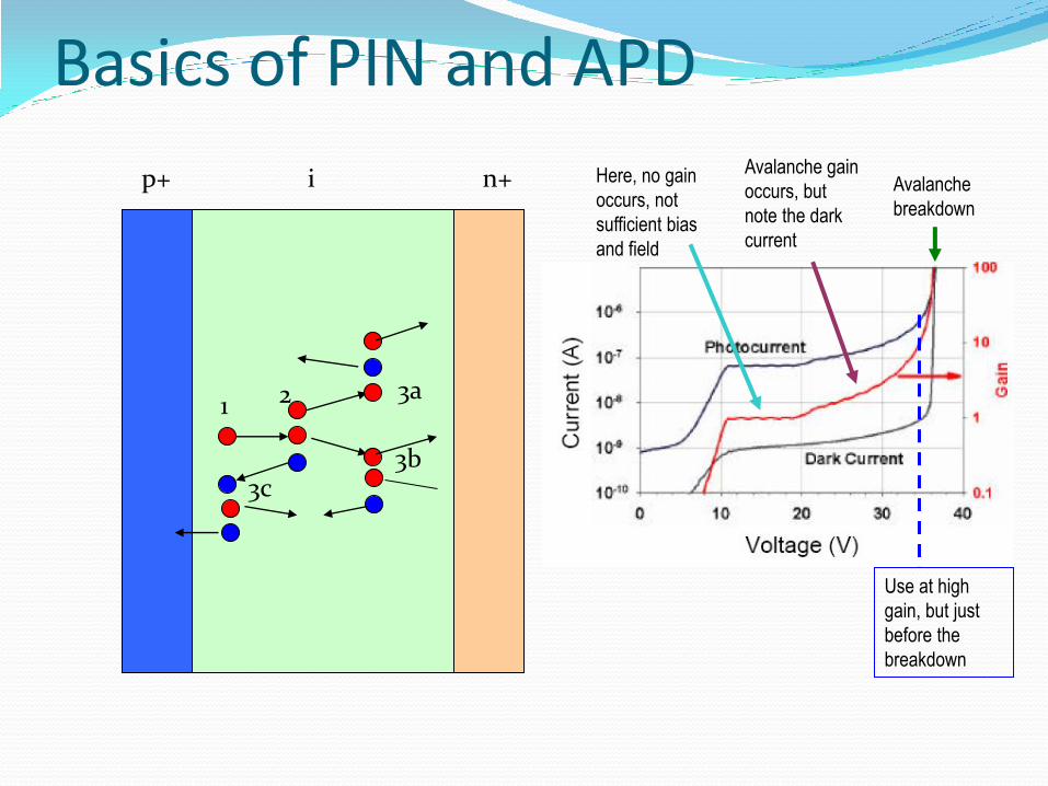
Basics of PIN and APD
p+ n+ i
1 2 3a
3b 3c
Here, no gain
occurs, not
sufficient bias
and field
Avalanche gain
occurs, but
note the dark
current
Use at high
gain, but just
before the
breakdown
Avalanche
breakdown
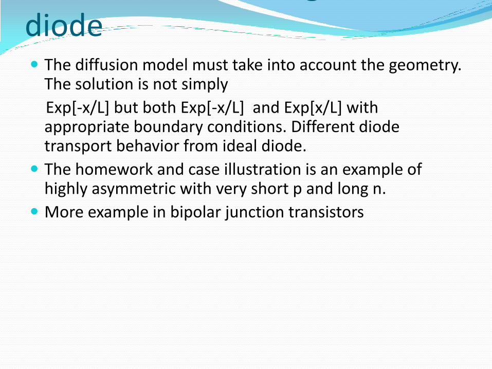
Short-based and long-based diode The diffusion model must take into account the geometry.
The solution is not simply
Exp[-x/L] but both Exp[-x/L] and Exp[x/L] with appropriate boundary conditions. Different diode transport behavior from ideal diode.
The homework and case illustration is an example of highly asymmetric with very short p and long n.
More example in bipolar junction transistors
Other junctions
Heterojunction
Schottky junction
Ohmic junction

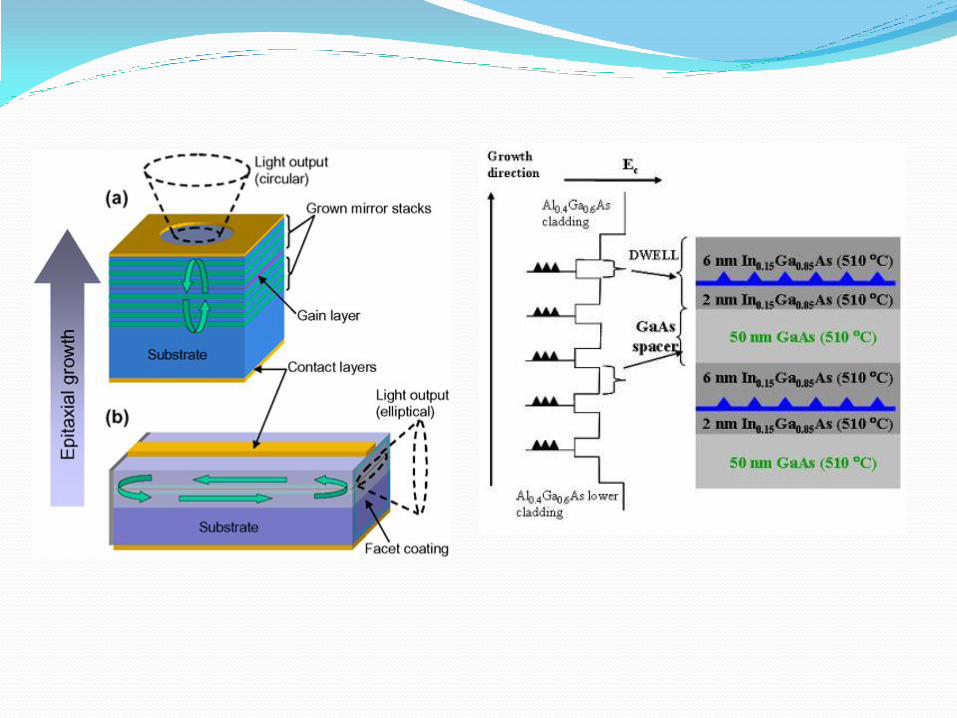
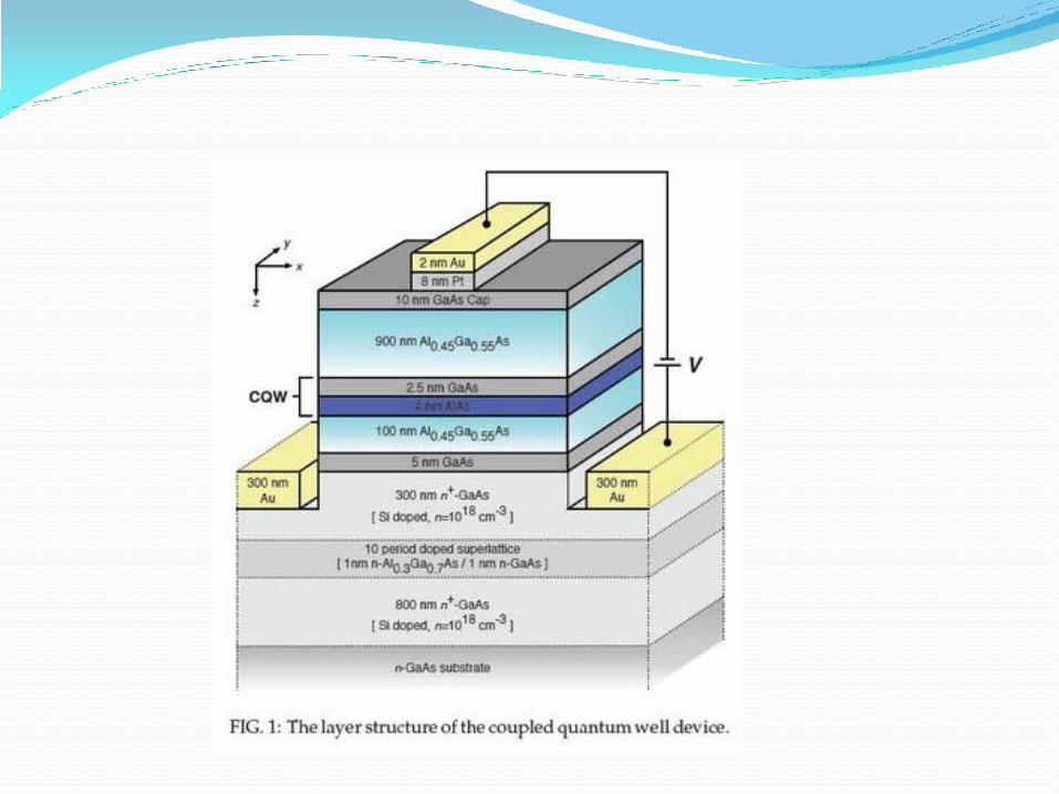
Junction fabrication Research paper
![$$ 5 - . 1 ) $ · ... PN junction, Junction Theory, VI characteristics of PN junction diode, Ideal diode, Static and Dynamic Resistance [1][2], Diode current equation[2],Diode notations](https://img.pdfslide.us/doc/110x75/5ae6f8997f8b9a29048e3147/-5-1-pn-junction-junction-theory-vi-characteristics-of-pn-junction.jpg)