Embed Size (px)
Citation preview

1
JUKI-730 Ver.3.0
386SX with LCD/CRT
& 4COM SBC
@Copyright 1998All Rights Reserved.Manual second edition Aug.01,1998The information in this document is subject to change without prior notice in orderto improve reliability, design and function and does not represent a commitment onthe part of the manufacturer.In no event will the manufacturer be liable for direct, indirect, special, incidental, orconsequential damages arising out of the use or inability to use the product ordocumentation, even if advised of the possibility of such damages.This document contains proprietary information protected by copyright. All rightsare reserved. No part of this manual may be reproduced by any mechanical,electronic, or other means in any form without prior written permission of themanufacturer.TrademarksJUKI-730 is registered trademarks of Acquire Inc., PC/104 is trademarked ofPC/104 Consortium, IBM PC is a registered trademark of International BusinessMachines Corporation. Intel is a registered trademark of Intel Corporation. AMI isregistered trademarks of American Megatrends, Inc. Other product namesmentioned herein are used for identification purposes only and may be trademarksand/or registered trademarks of their respective companies.

3
Contents
1. Introduction .......................................................... 3
2. Installation ............................................................ 6
3. Connection ......................................................... 13
4. AMI BIOS Setup................................................. 20
Appendix A. E2KEY Function ................................ 22
Appendix B. Watch-Dog Timer .............................. 24
Appendix C. Panel Support List ............................. 25

4
1
Introduction
Welcome to the JUKI-730 386SX with LCD/CRT/4COM SingleBoard Computer. The JUKI-730 is an ISA with PC/104 formfactor board, which comes equipped with ALI 6117 (includes386SX CPU) and advanced high-performance multi-mode I/O,designed for the system manufacturers, integrators, or VARsthat want to provide all the performance, reliability, and qualityat a reasonable price.
An advanced high performance super AT I/O chip WindbondW83877F and SMC FDC37C669 are used in the JUKI-730board. Both on-chip UARTs are compatible with the NS16C550.And one COM port can be set in RS232,RS422,or RS485.The parallel port and IDE interface are compatible with IBMPC/AT and XT architecture's, as well as EPP and ECP.
The LCD/CRT controller is HMC HM86508 which can providethe LCD and CRT display at the same time. The LCD interfaceconnector is a 44-pin 2.0mm pitch type.
The most outstanding feature in the JUKI-730 is built-in PC/104expansion bus. Based on the PC/104 bus, you could easilyinstall over thousands of PC/104 modules from hundreds'vendors in the world. The JUKI-730 has external powerconnector that could let it connects with power supply directly. Itis more suitable for your standalone applications.
1.1 Specifications :
5
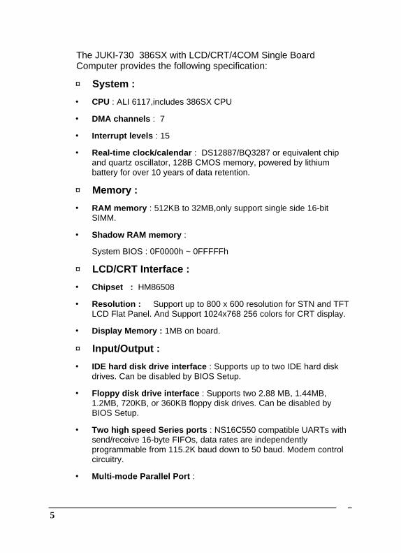
The JUKI-730 386SX with LCD/CRT/4COM Single BoardComputer provides the following specification:
♦ System :
• CPU : ALI 6117,includes 386SX CPU
• DMA channels : 7
• Interrupt levels : 15
• Real-time clock/calendar : DS12887/BQ3287 or equivalent chipand quartz oscillator, 128B CMOS memory, powered by lithiumbattery for over 10 years of data retention.
♦ Memory :
• RAM memory : 512KB to 32MB,only support single side 16-bitSIMM.
• Shadow RAM memory :
System BIOS : 0F0000h ~ 0FFFFFh
♦ LCD/CRT Interface :
• Chipset : HM86508
• Resolution : Support up to 800 x 600 resolution for STN and TFTLCD Flat Panel. And Support 1024x768 256 colors for CRT display.
• Display Memory : 1MB on board.
♦ Input/Output :
• IDE hard disk drive interface : Supports up to two IDE hard diskdrives. Can be disabled by BIOS Setup.
• Floppy disk drive interface : Supports two 2.88 MB, 1.44MB,1.2MB, 720KB, or 360KB floppy disk drives. Can be disabled byBIOS Setup.
• Two high speed Series ports : NS16C550 compatible UARTs withsend/receive 16-byte FIFOs, data rates are independentlyprogrammable from 115.2K baud down to 50 baud. Modem controlcircuitry.
• Multi-mode Parallel Port :

6
Standard mode - IBM PC/XT, PC/AT, PS/2 compatible bi-directionalparallel port.
Enhanced mode - Enhanced parallel port ( EPP) compatible withIEEE 1284 specification.
High speed mode - Microsoft and Hewlett Packard extendedcapabilities port ( ECP), compatible with IEEE 1248 specification.
♦ Industrial features :
• Watch-dog timer : can be set by 1,2,10,20,110,or 220 secondsperiod. Reset or NMI was generated when CPU did not periodicallytrigger the timer. Your program use hex 043 and 443 to control thewatch-dog and generate a system reset.
• PC/104 expansion bus : A 64-pin and 40-pin, industrial embedded-PC bus standard.
• External power connector : 8-pin male connector ( Molex 6410series compatible)
• Keyboard connector : A 5-pin header on board and 6-pin mini-DINkeyboard connector is located on the mounting bracket.
♦ General :
• Power Consumption : +5V @ 1.53A ( 40MHz,8MB RAM)
• Operating Temperature : 0° ~ 55° C
• Humidity : 5% ~ 95%, non-condense
• Dimension: 180mm(W) x 122mm(L), standard AT form factor
1.2 What You Have
In addition to this User's Manual, the JUKI-730 package includesthe following items:
• JUKI-730 386SX with LCD/CRT/4COM Single BoardComputer
• RS-232/Printer Cable & RS-232 x 2 Cable
• FDD/HDD Cable
• 6-pin Mini-Din to 5-pin Din Keyboard Adapter Cable
7
2
Installation
This chapter describes how to install the JUKI-730. At first, thelayout of JUKI-730 is shown, and the unpacking information thatyou should be careful is described. The jumpers and switchessetting for the JUKI-730's configuration, such as CPU typeselection, system clock setting, and interrupt IRQ setting forserial ports and parallel port, are also included.
2.1 JUKI-730's Layout
< reference next page >

8
2.2 CPU Setting for JUKI-730 Ver. 3.0
9
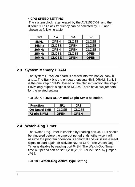
• CPU SPEED SETTING: The system clock is generated by the AV9155C-02, and the
different CPU clock frequency can be selected by JP3 and shown as following table:
JP3 1-2 3-4 5-6
8MHz OPEN CLOSE CLOSE16Mhz CLOSE OPEN CLOSE20MHz OPEN OPEN CLOSE25MHz CLOSE CLOSE OPEN40MHz CLOSE OPEN OPEN
2.3 System Memory DRAM
The system DRAM on board is divided into two banks, bank 0and 1. The Bank 0 is the on board optional 4MB DRAM. Bank 1is the one 72-pin SIMM. Based on the chipset function the 72-pinSIMM only support single side DRAM. There have two jumpersfor the related setting.
• JP1/JP2 : 4MB DRAM and 72-pin SIMM selection
Function JP1 JP2 On Board 1MB CLOSE CLOSE 72-pin SIMM OPEN OPEN
2.4 Watch-Dog Timer
The Watch-Dog Timer is enabled by reading port 443H. It shouldbe triggered before the time-out period ends, otherwise it willassume the program operation is abnormal and will issue a resetsignal to start again, or activate NMI to CPU. The Watch-DogTimer is disable by reading port 043H. The Watch-Dog Timertime-out period can be set 1,2,10,20,110 or 220 sec. by jumperJP16.
• JP18 : Watch-Dog Active Type Setting
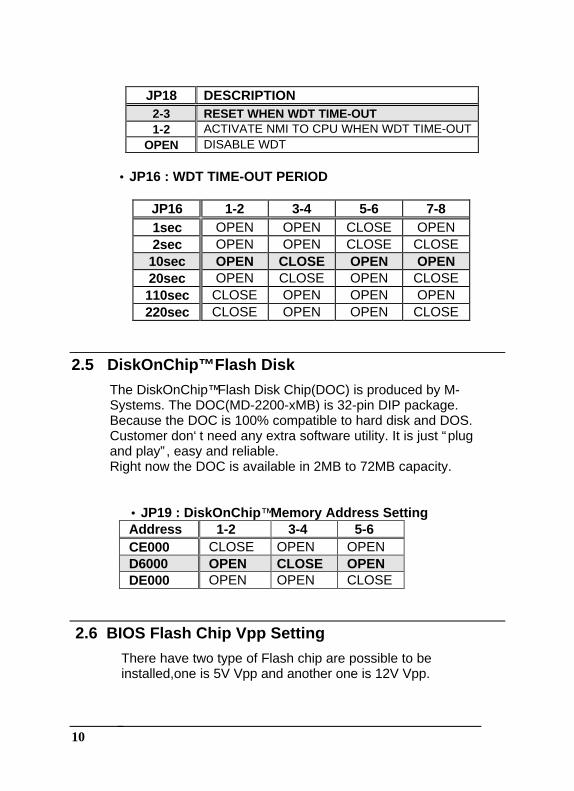
10
JP18 DESCRIPTION2-3 RESET WHEN WDT TIME-OUT1-2 ACTIVATE NMI TO CPU WHEN WDT TIME-OUT
OPEN DISABLE WDT • JP16 : WDT TIME-OUT PERIOD
JP16 1-2 3-4 5-6 7-81sec OPEN OPEN CLOSE OPEN2sec OPEN OPEN CLOSE CLOSE
10sec OPEN CLOSE OPEN OPEN20sec OPEN CLOSE OPEN CLOSE110sec CLOSE OPEN OPEN OPEN220sec CLOSE OPEN OPEN CLOSE
2.5 DiskOnChip™ Flash Disk
The DiskOnChip™ Flash Disk Chip(DOC) is produced by M- Systems. The DOC(MD-2200-xMB) is 32-pin DIP package. Because the DOC is 100% compatible to hard disk and DOS. Customer don‘ t need any extra software utility. It is just “plug and play” , easy and reliable. Right now the DOC is available in 2MB to 72MB capacity.
• JP19 : DiskOnChip™ Memory Address Setting Address 1-2 3-4 5-6 CE000 CLOSE OPEN OPEN D6000 OPEN CLOSE OPEN DE000 OPEN OPEN CLOSE
2.6 BIOS Flash Chip Vpp Setting
There have two type of Flash chip are possible to be installed,one is 5V Vpp and another one is 12V Vpp.

11
The Vpp is supplied when do the programming function.
Function JP24 5V Vpp 2-3 12V Vpp 1-2
2.7 Clear CMOS Setup
If want to clear the CMOS Setup(for example forgot the password you should clear the setup and then set the password again.),you should close the JP13 about 3 seconds, then open again. Then take Set back to normal operation mode take off the jumper. If the RTC Chip is Dallas DS12B887 you should do the procedure when the board is power on.
• JP13 : Clear CMOS Setup (Reserve Function)
JP13 DESCRIPTION OPEN Normal Operation CLOSE Clear CMOS Setup

12
2.8 COM3(CN1) RS232/422/485 Setting
The COM3 can be set in RS232 or RS422/ RS485 interface by the Jumper JP20/JP23. If choose RS422/485 then will need the JP21 to set again for RS422 or RS485.
• JP23 : COM3 RS-232 or RS-422/485 setting
Description JP23 JP20 RS-232 1-9 close
3-10 close 5-11 close 7-12 close
2-3
RS-422or RS-485
1-2 close3-4 close5-6 close7-8 close
1-2
• JP21 : COM3 RS-422 or RS-485 setting
JP21 DESCRIPTION 2-3 RS-422 1-2 RS-485
2.9 COM3/COM4 RI Pin Setting
The COM3 and COM4 can supply +5V or +12V power to the serial devices via RI pin(Pin 9) of the COM port connector. The max. current is 1A with fuse protection for the total two connector’ s 5V/12V output..
• JP9/JP29 : COM3(CN1),Pin 9 RI signal or 5V/12V output selection
Function JP9 JP29 RI Signal 2-3 1-2 5V 1-2 1-2 12V 1-2 2-3
13
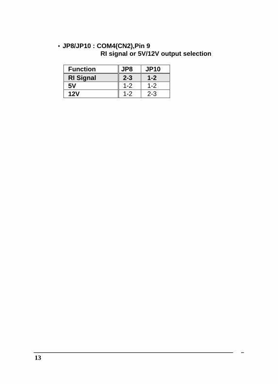
• JP8/JP10 : COM4(CN2),Pin 9 RI signal or 5V/12V output selection
Function JP8 JP10 RI Signal 2-3 1-2 5V 1-2 1-2 12V 1-2 2-3
14
3
Connection
This chapter describes how to connect peripherals, switches andindicators to the JUKI-730 board. You can access most of theconnectors from the top of the board while it is installed in thechassis.
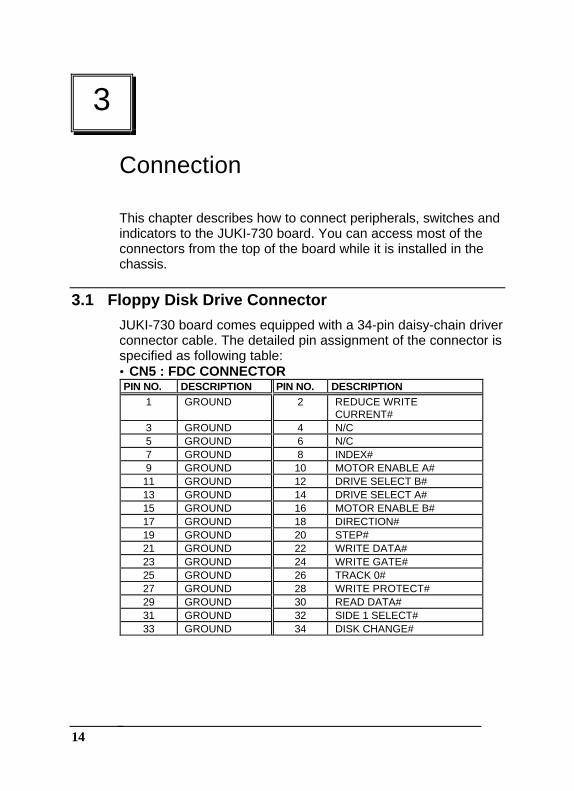
3.1 Floppy Disk Drive Connector
JUKI-730 board comes equipped with a 34-pin daisy-chain driverconnector cable. The detailed pin assignment of the connector isspecified as following table:• CN5 : FDC CONNECTORPIN NO. DESCRIPTION PIN NO. DESCRIPTION
1 GROUND 2 REDUCE WRITECURRENT#
3 GROUND 4 N/C5 GROUND 6 N/C7 GROUND 8 INDEX#9 GROUND 10 MOTOR ENABLE A#11 GROUND 12 DRIVE SELECT B#13 GROUND 14 DRIVE SELECT A#15 GROUND 16 MOTOR ENABLE B#17 GROUND 18 DIRECTION#19 GROUND 20 STEP#21 GROUND 22 WRITE DATA#23 GROUND 24 WRITE GATE#25 GROUND 26 TRACK 0#27 GROUND 28 WRITE PROTECT#29 GROUND 30 READ DATA#31 GROUND 32 SIDE 1 SELECT#33 GROUND 34 DISK CHANGE#

15
3.2 IDE Disk Drive Connector
You can attach two IDE( Integrated Device Electronics) harddisk drives to the JUKI-730 internal controller. The board comesequipped with a 40-pin flat-cable connector. The detailed pinassignment of the connector is specified as following table:
• CN4: IDE Interface ConnectorPIN NO. DESCRIPTION PIN NO. DESCRIPTION
1 RESET# 2 GROUND3 DATA 7 4 DATA 85 DATA 6 6 DATA 97 DATA 5 8 DATA 109 DATA 4 10 DATA 1111 DATA 3 12 DATA 1213 DATA 2 14 DATA 1315 DATA 1 16 DATA 1417 DATA 0 18 DATA 1519 GROUND 20 N/C21 N/C 22 GROUND23 IOW# 24 GROUND25 IOR# 26 GROUND27 N/C 28 BALE - DEFAULT29 N/C 30 GROUND - DEFAULT31 INTERRUPT 32 IOCS16#-DEFAULT33 SA1 34 N/C35 SA0 36 SA237 HDC CS0# 38 HDC CS1#39 HDD ACTIVE# 40 GROUND
3.3 Parallel Port
This port is usually connected to a printer, The JUKI-730 includes an on-board parallel port, accessed through a 26-pin flat-cable connector CN12.The detailed pin assignment of the connector is specified as followingtable:
• CN12 : Parallel Port Connector
16
PINNO.
DESCRIPTION PINNO.
DESCRIPTION
1 STROBE# 2 DATA 03 DATA 1 4 DATA 25 DATA 3 6 DATA 47 DATA 5 8 DATA 69 DATA 7 10 ACKNOWLEDGE11 BUSY 12 PAPER EMPTY13 PRINTER SELECT 14 AUTO FORM FEED #15 ERROR# 16 INITIALIZE17 PRINTER SELECT LN# 18 GROUND19 GROUND 20 GROUND21 GROUND 22 GROUND23 IOW# 24 GROUND25 GROUND
3.4 Serial Ports
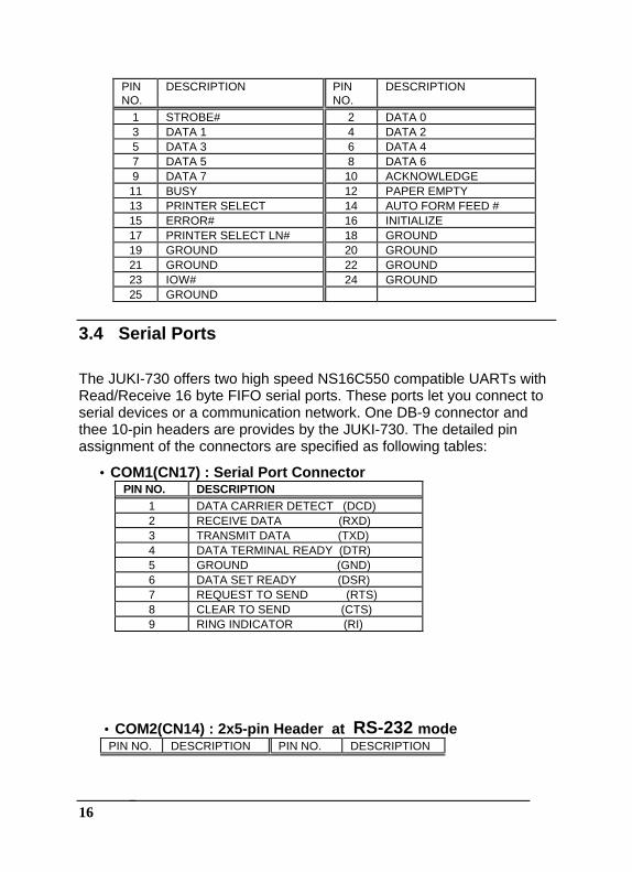
The JUKI-730 offers two high speed NS16C550 compatible UARTs withRead/Receive 16 byte FIFO serial ports. These ports let you connect toserial devices or a communication network. One DB-9 connector andthee 10-pin headers are provides by the JUKI-730. The detailed pinassignment of the connectors are specified as following tables:
• COM1(CN17) : Serial Port ConnectorPIN NO. DESCRIPTION
1 DATA CARRIER DETECT (DCD)2 RECEIVE DATA (RXD)3 TRANSMIT DATA (TXD)4 DATA TERMINAL READY (DTR)5 GROUND (GND)6 DATA SET READY (DSR)7 REQUEST TO SEND (RTS)8 CLEAR TO SEND (CTS)9 RING INDICATOR (RI)
• COM2(CN14) : 2x5-pin Header at RS-232 modePIN NO. DESCRIPTION PIN NO. DESCRIPTION
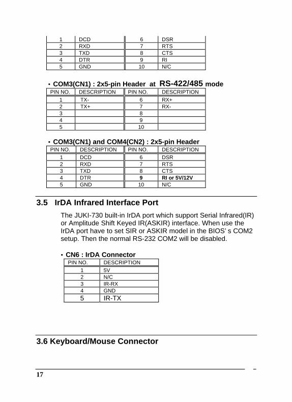
17
1 DCD 6 DSR2 RXD 7 RTS3 TXD 8 CTS4 DTR 9 RI5 GND 10 N/C
• COM3(CN1) : 2x5-pin Header at RS-422/485 modePIN NO. DESCRIPTION PIN NO. DESCRIPTION
1 TX- 6 RX+2 TX+ 7 RX-3 8 4 9 5 10
• COM3(CN1) and COM4(CN2) : 2x5-pin HeaderPIN NO. DESCRIPTION PIN NO. DESCRIPTION
1 DCD 6 DSR2 RXD 7 RTS3 TXD 8 CTS4 DTR 9 RI or 5V/12V5 GND 10 N/C
3.5 IrDA Infrared Interface Port
The JUKI-730 built-in IrDA port which support Serial Infrared(IR)or Amplitude Shift Keyed IR(ASKIR) interface. When use theIrDA port have to set SIR or ASKIR model in the BIOS’ s COM2setup. Then the normal RS-232 COM2 will be disabled.
• CN6 : IrDA ConnectorPIN NO. DESCRIPTION
1 5V2 N/C3 IR-RX4 GND
5 IR-TX
3.6 Keyboard/Mouse Connector

18
The JUKI-730 provides two keyboard connectors. A 5-pin headerconnector CN18 supports passive backplane applications.Another one is a 6-pin Mini-DIN connector CN19 on the boardmounting bracket for single board computer applications.
• CN18 : 5-pin Header Keyboard ConnectorPIN NO. DESCRIPTION
1 KEYBOARD CLOCK2 KEYBOARD DATA3 N/C4 GROUND5 +5V
• CN19/16 : 6-pin Mini-DIN Keyboard/Mouse ConnectorPIN NO. DESCRIPTION
1 KEYBOARD DATA MOUSE DATA2 N/C N/C3 GROUND GROUND4 +5V +5V5 KEYBOARD CLOCK MOUSE CLOCK6 N/C N/C
3.7 External Switches and Indicators
There are many external switches and indicators for monitoringand controlling your CPU board. These features are completelyoptional install them if you need them. The detailed pinassignment of the connectors is specified as following table:
• CN7 : RESET BUTTONPIN NO. DESCRIPTION
1 EXTERNAL RESET2 GROUND
• CN11 : IDE LED connectorPIN-NO DESCRIPTION
1 +5V2 HDD ACTIVE#
• CN8 : POWER LED & KEYLOCKPIN NO. DESCRIPTION
1 POWER LED ANODE
19
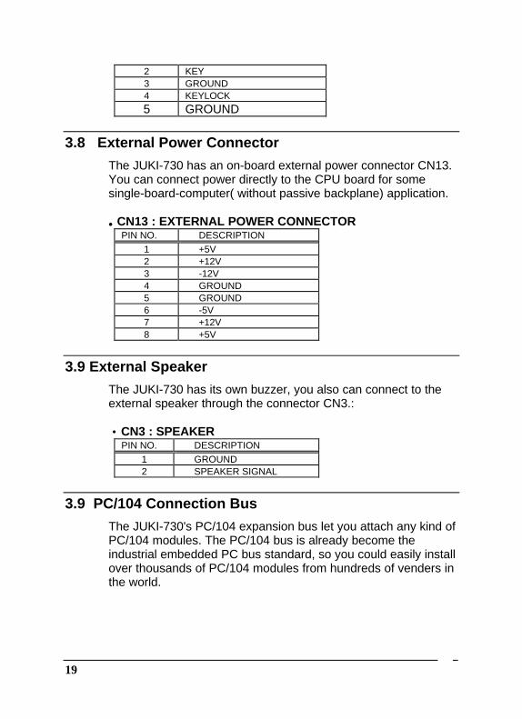
2 KEY3 GROUND4 KEYLOCK
5 GROUND
3.8 External Power Connector
The JUKI-730 has an on-board external power connector CN13.You can connect power directly to the CPU board for somesingle-board-computer( without passive backplane) application.
• CN13 : EXTERNAL POWER CONNECTORPIN NO. DESCRIPTION
1 +5V2 +12V3 -12V4 GROUND5 GROUND6 -5V7 +12V8 +5V
3.9 External Speaker
The JUKI-730 has its own buzzer, you also can connect to theexternal speaker through the connector CN3.:
• CN3 : SPEAKERPIN NO. DESCRIPTION
1 GROUND2 SPEAKER SIGNAL
3.9 PC/104 Connection Bus
The JUKI-730's PC/104 expansion bus let you attach any kind ofPC/104 modules. The PC/104 bus is already become theindustrial embedded PC bus standard, so you could easily installover thousands of PC/104 modules from hundreds of venders inthe world.

20
NOTE : JUKI-730 allows directly plug in PC/104 module,don‘ t need PC/104 Connection Kit.
3.10 LCD Interface Connector
The JUKI-730 provides a 2x22-pin connector for the LCD flatpanel interface. • CN20: LCD Interface Connector
PIN NO. DESCRIPTION PIN NO. DESCRIPTION
1 +12V 2 +12V3 GND 4 GND5 +5V 6 +5V7 FPVEE 8 GND9 P0 10 P111 P2 12 P313 P4 14 P515 P6 16 P717 P8 18 P919 P10 20 P1121 P12 22 P1323 P14 24 P1525 P16 26 P1727 P18 28 P1929 P20 30 P2131 P22 32 P2333 GND 34 GND35 SHFCLK 36 FLM37 M 38 LP39 GND 40 ENABLK41 GND 42 N/C43 FPVDD 44 5V
4
AMI BIOS Setup
21
The JUKI-730 use AMI BIOS for system configuration, and theAMI BIOS setup program is designed to provide maximumflexibility in configuring the system by offering various optionswhich may be selected for end-user requirements. This chapteris written to assist you in the proper usage of these features.
4.1 Getting Start
When the system is powered on, the BIOS will enter the Power-On-Self-Test routines. These routines will be executed forSystem Test and Initialization and System ConfigurationVerification. After the POST routines are completed, thefollowing message appears :
" Hit < Del>, if you want to run SETUP"To access AMI BIOS Setup program, press <Del> key.
4.2 Standard CMOS Setup
Standard CMOS Setup is the first option on the main menu.The standard CMOS setup utility is used to configure thefollowing features :¡ EDate/Time,¡ EHard Disk Type,¡ EFloppy Disk Type,All of these features are almost the same as common, so we donot describe more detailed in here.
4.3 Advanced CMOS Setup
When you enter the Advanced CMOS Setup, this Setup programis equipped with a series of help screens, accessed by <F1> key,which will display the options available for a particularconfiguration features.All the items on the left side of the screen are very common,they will not be mentioned here. Here, we just focus on somespecial items which are in ROCKY-318 board only. These itemsare specified as following :

22
¡ EOn-board IDE Controller : The IDE hard disk drive can beEnable or Disable by this item. When you do notneed hard disk, the IDE controller can be disabled.
¡ EOn-board Floppy Controller : The floppy disk drive can beEnable or Disable by this item. When you do notneed floppy disk, the FDD controller can bedisabled.
¡ ESerial Port 1 : The options are Disable, 3E8,2F8 ,or 3F8. Youcan set the I/O address of the serial port ( COMA)or disable it.
¡ ESerial Port 2 : The options are Disable, 2E8,3F8,or 2F8. Youcan set the I/O address of the serial port 1( COMB) or disable it.
¡ EParallel Port : The options are Disable, 3BC, 378 or 278. Youcan set the I/O address of the parallel port ordisable it.
¡ EParallel Port Mode : ROCKY-318 providesEPP,ECP,ECP+EPP, and Normal Mode.
Primary Display : You could set VGA/EGA, CGA40x25, CGA80x25, Mono or Absent. When set Absent the ROCKY-318 will not check the display adapter when power on the system.System Keyboard : You could set Present or Absent. When set Absent the ROCKY-318 will not check the display adapter when power on the system.
Appendix A. E2 Key™ Function
The JUKI-730 provides an outstanding E2KEY™ function for
system integrator. Based on the E2KEY™ you could free to store
the ID Code, Pass Word, or Critical Data in the 1Kbit EEPROM.
23
Because the EEPROM is nonvolatile memory, you don’ t have toworry the losing of the very important data.
Basically the E2KEY™ is based on a 1Kbit EEPROM which is
configured to 64 words(from 0 to 63). You could access(read orwrite) each word at any time.
When you start to use the E2KEY™ you should have the utility in
the package. The software utility will include four files as follows, README.DOC E2KEY.OBJ EKEYDEMO.C EKEYDEMO.EXE.
The E2KEY.OBJ provides two library function for user tointegrate their application with E
2KEY™ function. These library
(read_e2key and write_e2key) are written and compiled in Cformat. Please check the following statement, then you will knowhow to implement it easily.
unsigned int read_e2key(unsigned int address)/* This function will return the E
2KEY™’ s data at address. The
address range is from 0 to 63. Return data is one word,16 bits */void write_e2key(unsigned int address,unsigned data)/* This function will write the given data to E
2KEY™ at address.
The address range is from 0 to 63. The data value is from 0 to0xffff. */
To easy start to use the function, please refer the includeEKEYDEMO.C code at first.
Please note the E2KEY™ function is based on the working of
parallel port. So you should enable the ROCKY-318’ s parallelport, otherwise will be not working.

24
Appendix B. Watch-Dog Timer
The Watch-Dog Timer is provided to ensure that standalonesystems can always recover from catastrophic conditions thatcaused the CPU to crash. This condition may have occurred byexternal EMI or a software bug. When the CPU stops workingcorrectly, hardware on the board will either perform a hardwarereset (cold boot) or a non-maskable interrupt (NMI) to bring thesystem back to a known state.
25
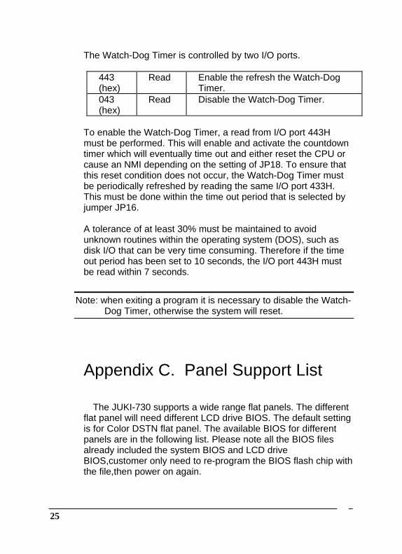
The Watch-Dog Timer is controlled by two I/O ports.
443(hex)
Read Enable the refresh the Watch-DogTimer.
043(hex)
Read Disable the Watch-Dog Timer.
To enable the Watch-Dog Timer, a read from I/O port 443Hmust be performed. This will enable and activate the countdowntimer which will eventually time out and either reset the CPU orcause an NMI depending on the setting of JP18. To ensure thatthis reset condition does not occur, the Watch-Dog Timer mustbe periodically refreshed by reading the same I/O port 433H.This must be done within the time out period that is selected byjumper JP16.
A tolerance of at least 30% must be maintained to avoidunknown routines within the operating system (DOS), such asdisk I/O that can be very time consuming. Therefore if the timeout period has been set to 10 seconds, the I/O port 443H mustbe read within 7 seconds.
Note: when exiting a program it is necessary to disable the Watch-Dog Timer, otherwise the system will reset.
Appendix C. Panel Support List
The JUKI-730 supports a wide range flat panels. The differentflat panel will need different LCD drive BIOS. The default settingis for Color DSTN flat panel. The available BIOS for differentpanels are in the following list. Please note all the BIOS filesalready included the system BIOS and LCD driveBIOS,customer only need to re-program the BIOS flash chip withthe file,then power on again.
26
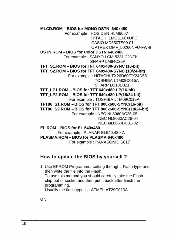
MLCD.ROM – BIOS for MONO DSTN 640x480 For example : HOSIDEN HLM6667 HITACHI LMG5160XUFC CASIO MD650TS00-01 OPTREX DMF_50260NFU-FW-8DSTN.ROM – BIOS for Color DSTN 640x480 For example : SANYO LCM-5331-22NTK SHARP LM64C35PTFT_S1.ROM – BIOS for TFT 640x480-SYNC (16-bit)TFT_S2.ROM – BIOS for TFT 640x480-SYNC (18/24-bit) For example : HITACHI TX26D60/TX24D55 TOSHIBA LTM09C015A SHARP LQ10D321TFT_LP1.ROM – BIOS for TFT 640x480-LP(16-bit)TFT_LP2.ROM – BIOS for TFT 640x480-LP(16/24-bit) For example : TOSHIBA LTM09C015ATFT86_S1.ROM – BIOS for TFT 800x600-SYNC(16-bit)TFT86_S2.ROM – BIOS for TFT 800x600-SYNC(18/24-bit) For example : NEC NL8060AC26-05 NEC NL8060AC26-04 NEC NL8060BC31-02EL.ROM – BIOS for EL 640x480 For example : PLANAR EL640.480-APLASMA.ROM – BIOS for PLASMA 640x480 For example : PANASONIC S817
How to update the BIOS by yourself ?
1. Use EPROM Programmer setting the right Flash type andthen write the file into the Flash.
To use this method,you should carefully take the Flash chip out of socket and then put it back after finish the programming. Usually the flash type is : ATMEL AT29C010A
Or,

27
2. There also have a utility (FLASH634.COM) and directly re-program the BIOS under DOS.For example :
C:>FLASH634 MLCD.ROM