Embed Size (px)
Citation preview
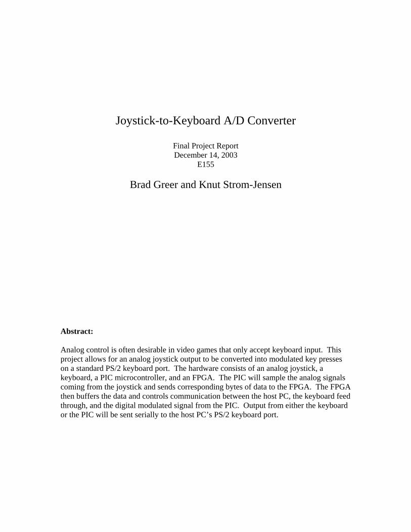
Joystick-to-Keyboard A/D Converter
Final Project Report December 14, 2003
E155
Brad Greer and Knut Strom-Jensen Abstract: Analog control is often desirable in video games that only accept keyboard input. This project allows for an analog joystick output to be converted into modulated key presses on a standard PS/2 keyboard port. The hardware consists of an analog joystick, a keyboard, a PIC microcontroller, and an FPGA. The PIC will sample the analog signals coming from the joystick and sends corresponding bytes of data to the FPGA. The FPGA then buffers the data and controls communication between the host PC, the keyboard feed through, and the digital modulated signal from the PIC. Output from either the keyboard or the PIC will be sent serially to the host PC’s PS/2 keyboard port.
Introduction Only a select few video games accept analog input. Normally, these include flight simulators and driving simulators. Many games, however, are only configured to accept digital keyboard input. Games like scrolling shooters could greatly benefit from the advantages of analog control. With this in mind, we intend to give the flexibility of analog control to a system that only accepts keyboard inputs.
Butto
n A
Sign
al
Analog Joystick
X-Axis Voltage
Y-Axis Voltage
10-Bit A/D Converter(PIC)
Y Bi
ts 9
:6
Modulation and SendingAlgorithms
(PIC)Button Signal Amplification
Button A Signal
Butto
n B
Sign
al
Button B Signal
FPGA
Dat
a By
te
Enab
le P
ulse
PS/2 Keyboard
Seria
l Dat
a
Host PC
Serial Data
Seria
l Clo
ck
Serial Clock
X Bi
ts 9
:6
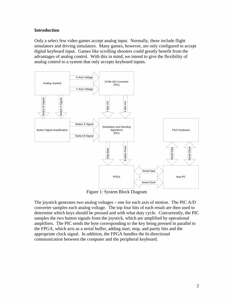
Figure 1: System Block Diagram
The joystick generates two analog voltages – one for each axis of motion. The PIC A/D converter samples each analog voltage. The top four bits of each result are then used to determine which keys should be pressed and with what duty cycle. Concurrently, the PIC samples the two button signals from the joystick, which are amplified by operational amplifiers. The PIC sends the byte corresponding to the key being pressed in parallel to the FPGA, which acts as a serial buffer, adding start, stop, and parity bits and the appropriate clock signal. In addition, the FPGA handles the bi-directional communication between the computer and the peripheral keyboard.
2
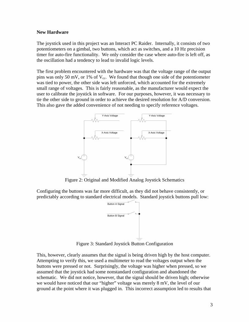
New Hardware The joystick used in this project was an Interact PC Raider. Internally, it consists of two potentiometers on a gimbal, two buttons, which act as switches, and a 10 Hz precision timer for auto-fire functionality. We only consider the case where auto-fire is left off, as the oscillation had a tendency to lead to invalid logic levels. The first problem encountered with the hardware was that the voltage range of the output pins was only 50 mV, or 1% of Vcc. We found that though one side of the potentiometer was tied to power, the other side was left unforced, which accounted for the extremely small range of voltages. This is fairly reasonable, as the manufacturer would expect the user to calibrate the joystick in software. For our purposes, however, it was necessary to tie the other side to ground in order to achieve the desired resolution for A/D conversion. This also gave the added convenience of not needing to specify reference voltages.
X-Axis Voltage
Y-Axis Voltage
Vcc
X-Axis Voltage
Y-Axis Voltage
Vcc
Figure 2: Original and Modified Analog Joystick Schematics
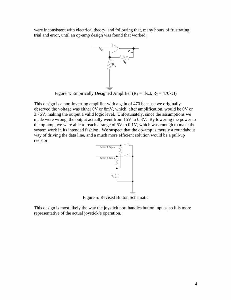
Configuring the buttons was far more difficult, as they did not behave consistently, or predictably according to standard electrical models. Standard joystick buttons pull low:
Button A Signal
Button B Signal
Figure 3: Standard Joystick Button Configuration
This, however, clearly assumes that the signal is being driven high by the host computer. Attempting to verify this, we used a multimeter to read the voltages output when the buttons were pressed or not. Surprisingly, the voltage was higher when pressed, so we assumed that the joystick had some nonstandard configuration and abandoned the schematic. We did not notice, however, that the signal should be driven high; otherwise we would have noticed that our “higher” voltage was merely 8 mV, the level of our ground at the point where it was plugged in. This incorrect assumption led to results that
3
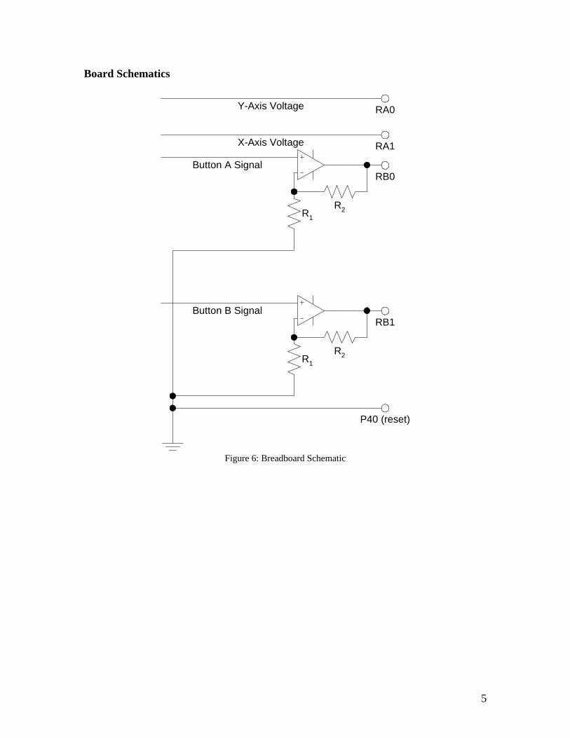
were inconsistent with electrical theory, and following that, many hours of frustrating trial and error, until an op-amp design was found that worked:
R1
Vout
R2
Vin
Figure 4: Empirically Designed Amplifier (R1 = 1kΩ, R2 = 470kΩ)
This design is a non-inverting amplifier with a gain of 470 because we originally observed the voltage was either 0V or 8mV, which, after amplification, would be 0V or 3.76V, making the output a valid logic level. Unfortunately, since the assumptions we made were wrong, the output actually went from 15V to 0.3V. By lowering the power to the op-amp, we were able to reach a range of 5V to 0.1V, which was enough to make the system work in its intended fashion. We suspect that the op-amp is merely a roundabout way of driving the data line, and a much more efficient solution would be a pull-up resistor:
Button A Signal
Button B Signal
Vcc
Figure 5: Revised Button Schematic
This design is most likely the way the joystick port handles button inputs, so it is more representative of the actual joystick’s operation.
4
Board Schematics
X-Axis Voltage
Y-Axis Voltage RA0
RA1
R1R2
Button A SignalRB0
R1R2
Button B SignalRB1
P40 (reset)
Figure 6: Breadboard Schematic
5
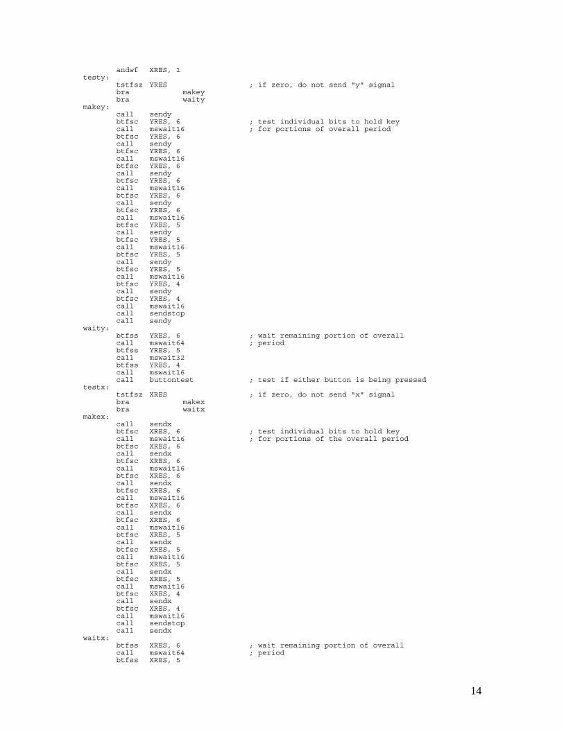
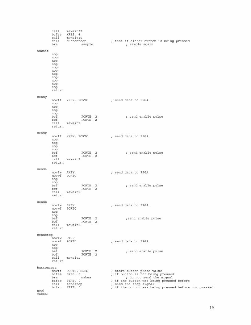
Microcontroller Design The PIC is programmed to sample two analog voltages, determine quadrant in which the joystick is located, and send pulse-width modulated signals corresponding to the amount of time the key is being pressed. The program begins by initializing all necessary control registers then entering into the main program loop. Each of the two analog voltages are sampled in series and saved in separate registers. Using the top bit of the y-axis result, the program determines whether the joystick’s position corresponds to the “up” key, or the “down” key. Likewise, the program determines whether to press the “left” key, or the “right” key. After determining which directions to press for each axis, a mask is applied to the results so that only the three relevant bits are considered. This is done so that if these three bits are zero, then the key will not be pressed at all, instead of being pressed for a very short period of time. The sending algorithm sends the signal for the key to be pressed, then waits an amount of time proportionate to the magnitude of the 3-bit number. After waiting, the program sends the “stop” signal for the key that was just pressed, and then waits the remainder of the period with no key being pressed. If the masked result is equal to zero, the sending algorithm is skipped, and the program waits the entirety of the period. Before proceeding to the sending algorithm for the second axis, the program checks the status of the buttons, and sends any necessary signals (start, continue, stop) based on their current and previous status. Then the program goes through the send and wait algorithms for the second axis, then samples the voltages again. Subroutines send*: All of the send methods are essentially the same, with the notable difference being the byte that is sent to the FPGA. First, the value is loaded into Port C, which is connected in parallel with the FPGA. After a couple of no-operations, the value in Port C will be stable, and the program sends a pulse on Port E, bit 2, which acts as an enable signal for the FPGA, and it begins sending the data. It would be possible to check for the FPGA feedback bit “good”, but instead the program simply waits 2 milliseconds, which is long enough for a byte to be sent serially. adwait: It takes 12 instruction cycles for the PIC to finish the A/D conversion, so this method executes no-operations for a long enough time for the result to be received. This time could not be productively used otherwise, so dealing with interrupts is unnecessary. uswait500: This method uses timer0, which is configured as an 8-bit timer running off of the instruction clock (500 KHz) with no prescale. It does not use interrupts, but does loop and watch for the interrupt flag when the timer rolls over, and then branching out of the loop. This results in a wait of approximately 500 microseconds. All other wait routines call this routine a number of times. buttontest: This method samples the value of the two button inputs, sends the appropriate signals, and stores their previous values. This way, if the button was not being pressed previously, the program will not tell it to stop sending if it is not being pressed now.
6
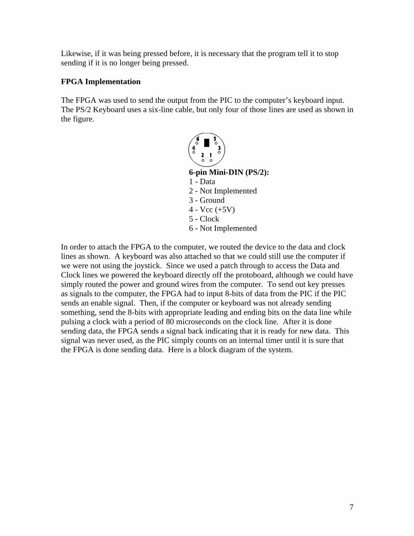
Likewise, if it was being pressed before, it is necessary that the program tell it to stop sending if it is no longer being pressed. FPGA Implementation The FPGA was used to send the output from the PIC to the computer’s keyboard input. The PS/2 Keyboard uses a six-line cable, but only four of those lines are used as shown in the figure.
6-pin Mini-DIN (PS/2): 1 - Data 2 - Not Implemented 3 - Ground 4 - Vcc (+5V) 5 - Clock 6 - Not Implemented
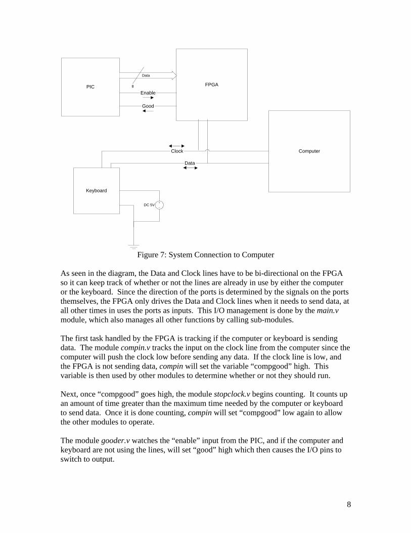
In order to attach the FPGA to the computer, we routed the device to the data and clock lines as shown. A keyboard was also attached so that we could still use the computer if we were not using the joystick. Since we used a patch through to access the Data and Clock lines we powered the keyboard directly off the protoboard, although we could have simply routed the power and ground wires from the computer. To send out key presses as signals to the computer, the FPGA had to input 8-bits of data from the PIC if the PIC sends an enable signal. Then, if the computer or keyboard was not already sending something, send the 8-bits with appropriate leading and ending bits on the data line while pulsing a clock with a period of 80 microseconds on the clock line. After it is done sending data, the FPGA sends a signal back indicating that it is ready for new data. This signal was never used, as the PIC simply counts on an internal timer until it is sure that the FPGA is done sending data. Here is a block diagram of the system.
7
Keyboard
DC 5V
FPGAPICEnable
Data
8
Computer
Data
Clock
Good
Figure 7: System Connection to Computer
As seen in the diagram, the Data and Clock lines have to be bi-directional on the FPGA so it can keep track of whether or not the lines are already in use by either the computer or the keyboard. Since the direction of the ports is determined by the signals on the ports themselves, the FPGA only drives the Data and Clock lines when it needs to send data, at all other times in uses the ports as inputs. This I/O management is done by the main.v module, which also manages all other functions by calling sub-modules. The first task handled by the FPGA is tracking if the computer or keyboard is sending data. The module compin.v tracks the input on the clock line from the computer since the computer will push the clock low before sending any data. If the clock line is low, and the FPGA is not sending data, compin will set the variable “compgood” high. This variable is then used by other modules to determine whether or not they should run. Next, once “compgood” goes high, the module stopclock.v begins counting. It counts up an amount of time greater than the maximum time needed by the computer or keyboard to send data. Once it is done counting, compin will set “compgood” low again to allow the other modules to operate. The module gooder.v watches the “enable” input from the PIC, and if the computer and keyboard are not using the lines, will set “good” high which then causes the I/O pins to switch to output.
8
When “good” has gone high, and “enable” is also high, holder.v inputs 8 bits of data from the PIC. These 8 bits represent the scancodes for the PS/2 port. These 8 bits are held in registers until they are needed. Also enabled when “good” goes high is the module clocker.v, which counts out a period of 80 microseconds, the lowest clock speed at which the PS/2 port should run (although our tests shower some keyboards transmitting with slightly faster clocks). This clock is used to run the data output. The computer expects the keyboard to output the clock signal 5-25 microseconds after it outputs the data since the computer reads on the falling edge when the data would normally be changing. To accommodate this, the module delay.v forces the clock output from clocker through a series of registers to delay it the required amount of time. This is the clock sent out on the clock line, not the one directly from clocker. The module counter4.v is a 4 bit counter intended to count from 0 to10, in order to output the 11-bit packet of data to the computer. This module runs on the non-delayed clock. Finishing the data sending is packeter.v which uses the variable “count” from counter4 and goes through all the data bits of the packet sent to the computer. First it sends a low bit to indicate the data has started. Next it sends the scancode the FPGA received from the PIC from the most significant bit down too the least significant bit. Finally it sends a parity bit and a high bit to indicate the data is complete. Once “count” exceeds 10, “good” is set low by gooder and the FPGA is ready to send the next packet the PIC sends it. The module feedback.v takes a further delayed clock and checks to see if the clock output is being forced low by the computer. If it is, it stops the FPGA from sending data and waits for the next command from the PIC.
9
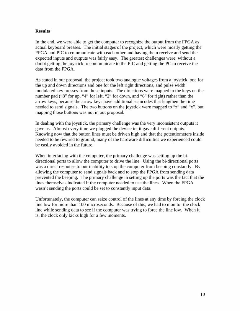
Results In the end, we were able to get the computer to recognize the output from the FPGA as actual keyboard presses. The initial stages of the project, which were mostly getting the FPGA and PIC to communicate with each other and having them receive and send the expected inputs and outputs was fairly easy. The greatest challenges were, without a doubt getting the joystick to communicate to the PIC and getting the PC to receive the data from the FPGA. As stated in our proposal, the project took two analogue voltages from a joystick, one for the up and down directions and one for the left right directions, and pulse width modulated key presses from those inputs. The directions were mapped to the keys on the number pad (“8” for up, “4” for left, “2” for down, and “6” for right) rather than the arrow keys, because the arrow keys have additional scancodes that lengthen the time needed to send signals. The two buttons on the joystick were mapped to “z” and “x”, but mapping those buttons was not in out proposal. In dealing with the joystick, the primary challenge was the very inconsistent outputs it gave us. Almost every time we plugged the device in, it gave different outputs. Knowing now that the button lines must be driven high and that the potentiometers inside needed to be rewired to ground, many of the hardware difficulties we experienced could be easily avoided in the future. When interfacing with the computer, the primary challenge was setting up the bi-directional ports to allow the computer to drive the line. Using the bi-directional ports was a direct response to our inability to stop the computer from beeping constantly. By allowing the computer to send signals back and to stop the FPGA from sending data prevented the beeping. The primary challenge in setting up the ports was the fact that the lines themselves indicated if the computer needed to use the lines. When the FPGA wasn’t sending the ports could be set to constantly input data. Unfortunately, the computer can seize control of the lines at any time by forcing the clock line low for more than 100 microseconds. Because of this, we had to monitor the clock line while sending data to see if the computer was trying to force the line low. When it is, the clock only kicks high for a few moments.
10
By checking to see if the clock is low when it should be high allows the FPGA to determine if the computer is trying to force the line low. The only problem is that the data the FPGA is trying to send is simply dropped and is never resent. Given time, a more efficient system could be implemented in which the FPGA resends the data. At present, the FPGA assumes the computer is pushing clock low if one clock that should be high is low. Since the clock sometimes stays low longer in its last cycle, the FPGA interprets this as the computer trying to send input even when it is not. This is not a problem normally, but can cause problems if we want to resend data. Thus to properly resend data, the FPGA would have to sample multiple time and make a decision based on multiple data points. Also, the PIC would have to be notified so that it does not try to send new data while the FPGA is resending old data. Not resending the data resulted in the somewhat erratic behavior of our device when sending many button presses to the computer. Sometimes the system speeds up and then slows down depending on how many packets are being dropped by the computer. The computer is likely dropping the packets because we are sending too many signals in too short a time, forcing the computer to halt inputs until it is ready for more. Sometimes the lost packets are the stop signals for the various button presses, resulting in the computer assuming that the key is still pressed and causing results after the joystick is no longer being pressed in any direction.
11
References [1] A. Chapweske, Adam’s Micro-Resources, http://panda.cs.ndsu.nodak.edu/~achapwes/PICmicro/[2] Op-Amp Varieties, http://hyperphysics.phy-astr.gsu.edu/hbase/electronic/opampvar.html[3] Texas Instruments, Precision Timer Data Sheet http://physics.gac.edu/~huber/classes/phy270/SpecSheets/lm555_ti.pdf[4] Standard Joystick Schematic http://www.hut.fi/Misc/Electronics/docs/joystick/pc_stick.gif Parts List Part Source Price Interact PC Raider Ebay $10.00 Mini-DIN 6 Pin Sockets (2)
Digi-Key $2.00
Keyboard Cable Digi-Key $3.00
12
Appendix A: PIC code ; JoyAD9.asm ; written on 12/06/03 by Brad Greer <[email protected]> ; Joystick A/D converter and keyboard output PWM controller ; use the 18F452 PIC microprocessor LIST p=18F452 include "p18f452.inc" ; define constants YON EQU 0x05 XON EQU 0x0D UKEY EQU 0xAE DKEY EQU 0x4E LKEY EQU 0xD6 RKEY EQU 0x2E AKEY EQU 0x58 BKEY EQU 0x44 STOP EQU 0x0F MASK EQU 0x70 ; define variables YKEY EQU 0x00 XKEY EQU 0x01 YRES EQU 0x02 XRES EQU 0x03 BRES EQU 0x04 STAT EQU 0x05 ; set interrupt branches org 0x0 bra init org 0x20 ; initialize control registers init: setf TRISA ; set port A to input setf TRISB ; set port B to input clrf TRISC ; set port C to output movlw 0x03 ; set port E, bits 0,1 to input movwf TRISE ; bit 2 to output movlw 0x42 movwf ADCON1 ; configure A/D converter movlw 0x48 movwf T0CON ; configure Timer0 sample: movlw YON ; sample y axis movwf ADCON0 call adwait ; wait for A/D to finish movff ADRESH, YRES ; move result movlw XON ; sample x axis movwf ADCON0 call adwait ; wait for A/D to finish movff ADRESH, XRES ; move result sety: btfsc YRES, 7 ; if result > 1/2 of maximum bra up ; set y axis key press to Up bra down ; else set y axis key press to Down up: movlw UKEY ; move Up to register storing y axis key movwf YKEY bra setx ; bypass Down down: comf YRES ; invert bits for accurate operation movlw DKEY ; move Down to register storing y axis key movwf YKEY setx: btfsc XRES, 7 ; if result > 1/2 of maximum bra left ; set X axis key press to Left bra right ; else set x axis key press to Right left: movlw LKEY ; move Left to register storing x axis key movwf XKEY bra mask ; bypass Right right: comf XRES ; invert bits for accurate operation movlw RKEY ; move Right to register storing x axis key movwf XKEY mask: movlw MASK andwf YRES, 1
13
andwf XRES, 1 testy: tstfsz YRES ; if zero, do not send "y" signal bra makey bra waity makey: call sendy btfsc YRES, 6 ; test individual bits to hold key call mswait16 ; for portions of overall period btfsc YRES, 6 call sendy btfsc YRES, 6 call mswait16 btfsc YRES, 6 call sendy btfsc YRES, 6 call mswait16 btfsc YRES, 6 call sendy btfsc YRES, 6 call mswait16 btfsc YRES, 5 call sendy btfsc YRES, 5 call mswait16 btfsc YRES, 5 call sendy btfsc YRES, 5 call mswait16 btfsc YRES, 4 call sendy btfsc YRES, 4 call mswait16 call sendstop call sendy waity: btfss YRES, 6 ; wait remaining portion of overall call mswait64 ; period btfss YRES, 5 call mswait32 btfss YRES, 4 call mswait16 call buttontest ; test if either button is being pressed testx: tstfsz XRES ; if zero, do not send "x" signal bra makex bra waitx makex: call sendx btfsc XRES, 6 ; test individual bits to hold key call mswait16 ; for portions of the overall period btfsc XRES, 6 call sendx btfsc XRES, 6 call mswait16 btfsc XRES, 6 call sendx btfsc XRES, 6 call mswait16 btfsc XRES, 6 call sendx btfsc XRES, 6 call mswait16 btfsc XRES, 5 call sendx btfsc XRES, 5 call mswait16 btfsc XRES, 5 call sendx btfsc XRES, 5 call mswait16 btfsc XRES, 4 call sendx btfsc XRES, 4 call mswait16 call sendstop call sendx waitx: btfss XRES, 6 ; wait remaining portion of overall call mswait64 ; period btfss XRES, 5
14
call mswait32 btfss XRES, 4 call mswait16 call buttontest ; test if either button is being pressed bra sample ; sample again adwait nop nop nop nop nop nop nop nop nop nop nop return sendy movff YKEY, PORTC ; send data to FPGA nop nop nop nop bsf PORTE, 2 ; send enable pulse bcf PORTE, 2 call mswait2 return sendx movff XKEY, PORTC ; send data to FPGA nop nop nop nop bsf PORTE, 2 ; send enable pulse bcf PORTE, 2 call mswait2 return senda movlw AKEY ; send data to FPGA movwf PORTC nop nop bsf PORTE, 2 ; send enable pulse bcf PORTE, 2 call mswait2 return sendb movlw BKEY ; send data to FPGA movwf PORTC nop nop bsf PORTE, 2 ;send enable pulse bcf PORTE, 2 call mswait2 return sendstop movlw STOP movwf PORTC ; send data to FPGA nop nop bsf PORTE, 2 ; send enable pulse bcf PORTE, 2 call mswait2 return buttontest movff PORTB, BRES ; store button-press value btfss BRES, 0 ; if button is not being pressed bra makea ; do not send the signal btfsc STAT, 0 ; if the button was being pressed before call sendstop ; send the stop signal btfsc STAT, 0 ; if the button was being pressed before (or pressed now) makea:
15
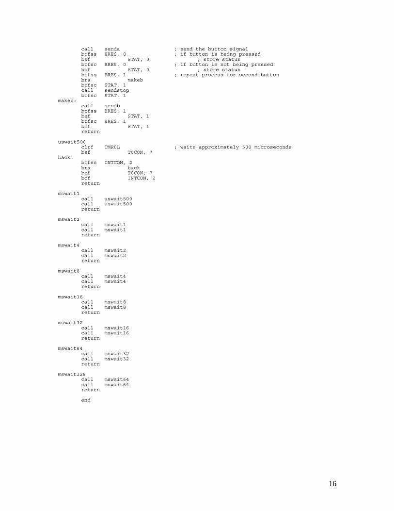
call senda ; send the button signal btfss BRES, 0 ; if button is being pressed bsf STAT, 0 ; store status btfsc BRES, 0 ; if button is not being pressed bcf STAT, 0 ; store status btfss BRES, 1 ; repeat process for second button bra makeb btfsc STAT, 1 call sendstop btfsc STAT, 1 makeb: call sendb btfss BRES, 1 bsf STAT, 1 btfsc BRES, 1 bcf STAT, 1 return uswait500 clrf TMR0L ; waits approximately 500 microseconds bsf T0CON, 7 back: btfss INTCON, 2 bra back bcf T0CON, 7 bcf INTCON, 2 return mswait1 call uswait500 call uswait500 return mswait2 call mswait1 call mswait1 return mswait4 call mswait2 call mswait2 return mswait8 call mswait4 call mswait4 return mswait16 call mswait8 call mswait8 return mswait32 call mswait16 call mswait16 return mswait64 call mswait32 call mswait32 return mswait128 call mswait64 call mswait64 return end
16
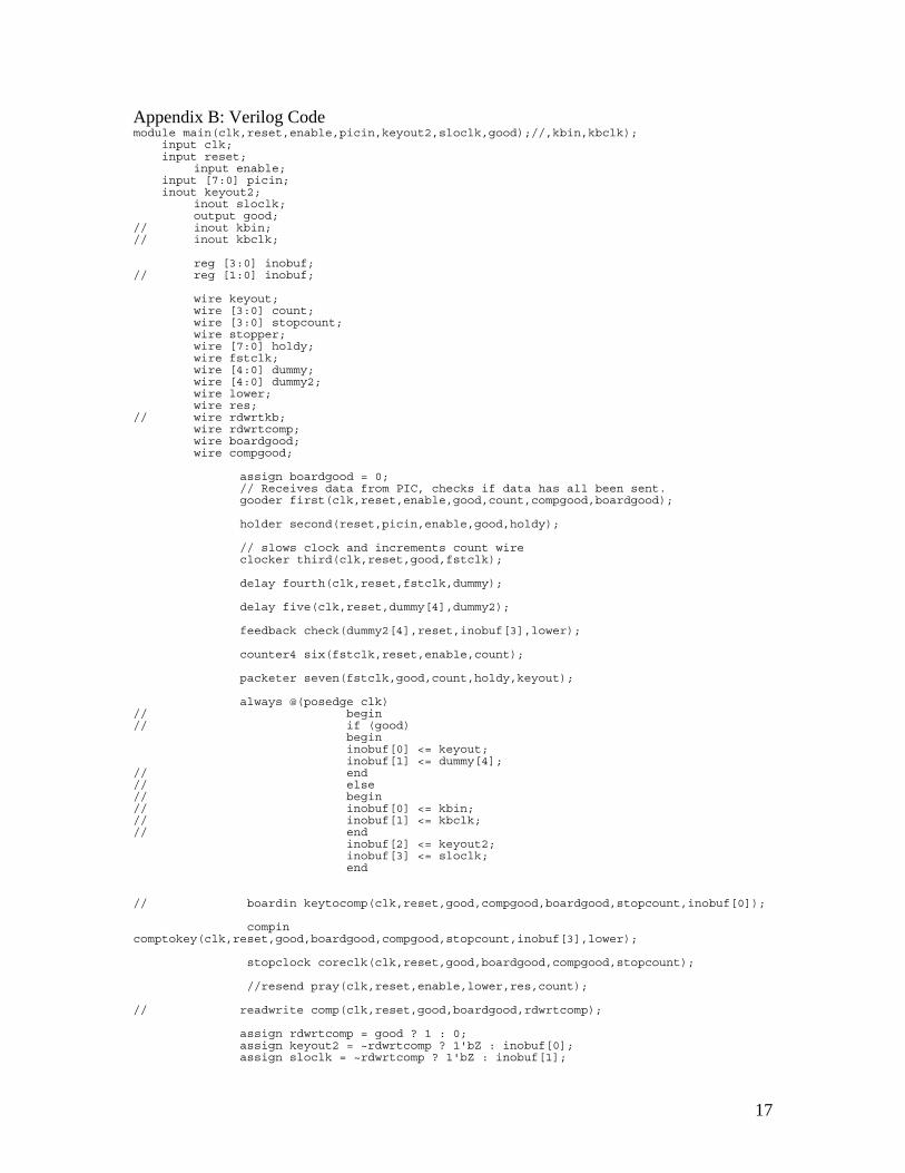
Appendix B: Verilog Code module main(clk,reset,enable,picin,keyout2,sloclk,good);//,kbin,kbclk); input clk; input reset; input enable; input [7:0] picin; inout keyout2; inout sloclk; output good; // inout kbin; // inout kbclk; reg [3:0] inobuf; // reg [1:0] inobuf; wire keyout; wire [3:0] count; wire [3:0] stopcount; wire stopper; wire [7:0] holdy; wire fstclk; wire [4:0] dummy; wire [4:0] dummy2; wire lower; wire res; // wire rdwrtkb; wire rdwrtcomp; wire boardgood; wire compgood; assign boardgood = 0; // Receives data from PIC, checks if data has all been sent. gooder first(clk,reset,enable,good,count,compgood,boardgood); holder second(reset,picin,enable,good,holdy); // slows clock and increments count wire clocker third(clk,reset,good,fstclk); delay fourth(clk,reset,fstclk,dummy); delay five(clk,reset,dummy[4],dummy2); feedback check(dummy2[4],reset,inobuf[3],lower); counter4 six(fstclk,reset,enable,count); packeter seven(fstclk,good,count,holdy,keyout); always @(posedge clk) // begin // if (good) begin inobuf[0] <= keyout; inobuf[1] <= dummy[4]; // end // else // begin // inobuf[0] <= kbin; // inobuf[1] <= kbclk; // end inobuf[2] <= keyout2; inobuf[3] <= sloclk; end // boardin keytocomp(clk,reset,good,compgood,boardgood,stopcount,inobuf[0]); compin comptokey(clk,reset,good,boardgood,compgood,stopcount,inobuf[3],lower); stopclock coreclk(clk,reset,good,boardgood,compgood,stopcount); //resend pray(clk,reset,enable,lower,res,count); // readwrite comp(clk,reset,good,boardgood,rdwrtcomp); assign rdwrtcomp = good ? 1 : 0; assign keyout2 = ~rdwrtcomp ? 1'bZ : inobuf[0]; assign sloclk = ~rdwrtcomp ? 1'bZ : inobuf[1];
17
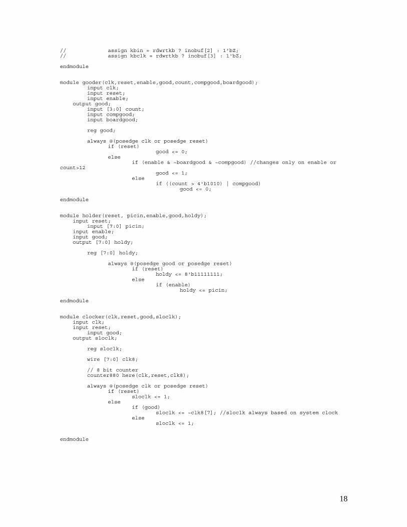
// assign kbin = rdwrtkb ? inobuf[2] : 1'bZ; // assign kbclk = rdwrtkb ? inobuf[3] : 1'bZ; endmodule module gooder(clk,reset,enable,good,count,compgood,boardgood); input clk; input reset; input enable; output good; input [3:0] count; input compgood; input boardgood; reg good; always @(posedge clk or posedge reset) if (reset) good <= 0; else if (enable & ~boardgood & ~compgood) //changes only on enable or count>12 good <= 1; else if ((count > 4'b1010) | compgood) good <= 0; endmodule module holder(reset, picin,enable,good,holdy); input reset; input [7:0] picin; input enable; input good; output [7:0] holdy; reg [7:0] holdy; always @(posedge good or posedge reset) if (reset) holdy <= 8'b11111111; else if (enable) holdy <= picin; endmodule module clocker(clk,reset,good,sloclk); input clk; input reset; input good; output sloclk; reg sloclk; wire [7:0] clk8; // 8 bit counter counter880 here(clk,reset,clk8); always @(posedge clk or posedge reset) if (reset) sloclk <= 1; else if (good) sloclk <= ~clk8[7]; //sloclk always based on system clock else sloclk <= 1; endmodule
18
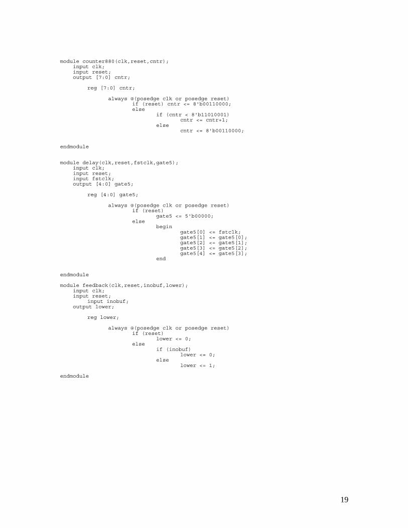
module counter880(clk,reset,cntr); input clk; input reset; output [7:0] cntr; reg [7:0] cntr; always @(posedge clk or posedge reset) if (reset) cntr <= 8'b00110000; else if (cntr < 8'b11010001) cntr <= cntr+1; else cntr <= 8'b00110000; endmodule module delay(clk,reset,fstclk,gate5); input clk; input reset; input fstclk; output [4:0] gate5; reg [4:0] gate5; always @(posedge clk or posedge reset) if (reset) gate5 <= 5'b00000; else begin gate5[0] <= fstclk; gate5[1] <= gate5[0]; gate5[2] <= gate5[1]; gate5[3] <= gate5[2]; gate5[4] <= gate5[3]; end endmodule module feedback(clk,reset,inobuf,lower); input clk; input reset; input inobuf; output lower; reg lower; always @(posedge clk or posedge reset) if (reset) lower <= 0; else if (inobuf) lower <= 0; else lower <= 1; endmodule
19
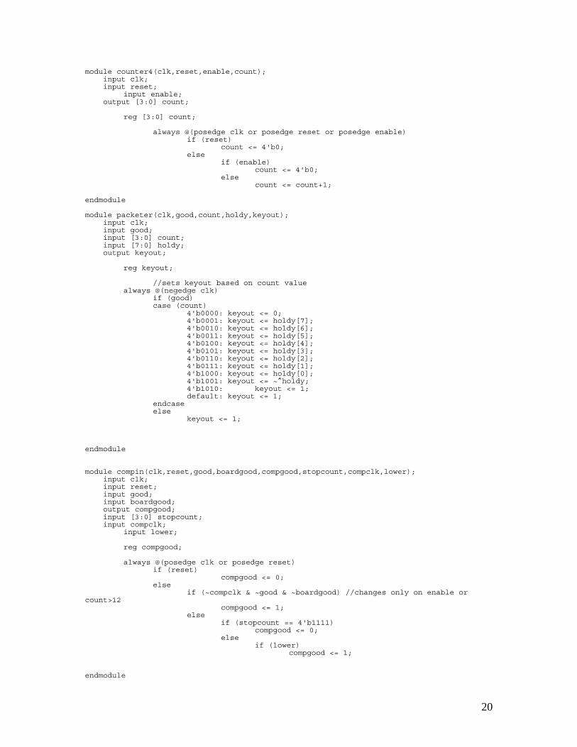
module counter4(clk,reset,enable,count); input clk; input reset; input enable; output [3:0] count; reg [3:0] count; always @(posedge clk or posedge reset or posedge enable) if (reset) count <= 4'b0; else if (enable) count <= 4'b0; else count <= count+1; endmodule module packeter(clk,good,count,holdy,keyout); input clk; input good; input [3:0] count; input [7:0] holdy; output keyout; reg keyout; //sets keyout based on count value always @(negedge clk) if (good) case (count) 4'b0000: keyout <= 0; 4'b0001: keyout <= holdy[7]; 4'b0010: keyout <= holdy[6]; 4'b0011: keyout <= holdy[5]; 4'b0100: keyout <= holdy[4]; 4'b0101: keyout <= holdy[3]; 4'b0110: keyout <= holdy[2]; 4'b0111: keyout <= holdy[1]; 4'b1000: keyout <= holdy[0]; 4'b1001: keyout <= ~^holdy; 4'b1010: keyout <= 1; default: keyout <= 1; endcase else keyout <= 1; endmodule module compin(clk,reset,good,boardgood,compgood,stopcount,compclk,lower); input clk; input reset; input good; input boardgood; output compgood; input [3:0] stopcount; input compclk; input lower; reg compgood; always @(posedge clk or posedge reset) if (reset) compgood <= 0; else if (~compclk & ~good & ~boardgood) //changes only on enable or count>12 compgood <= 1; else if (stopcount == 4'b1111) compgood <= 0; else if (lower) compgood <= 1; endmodule
20

21
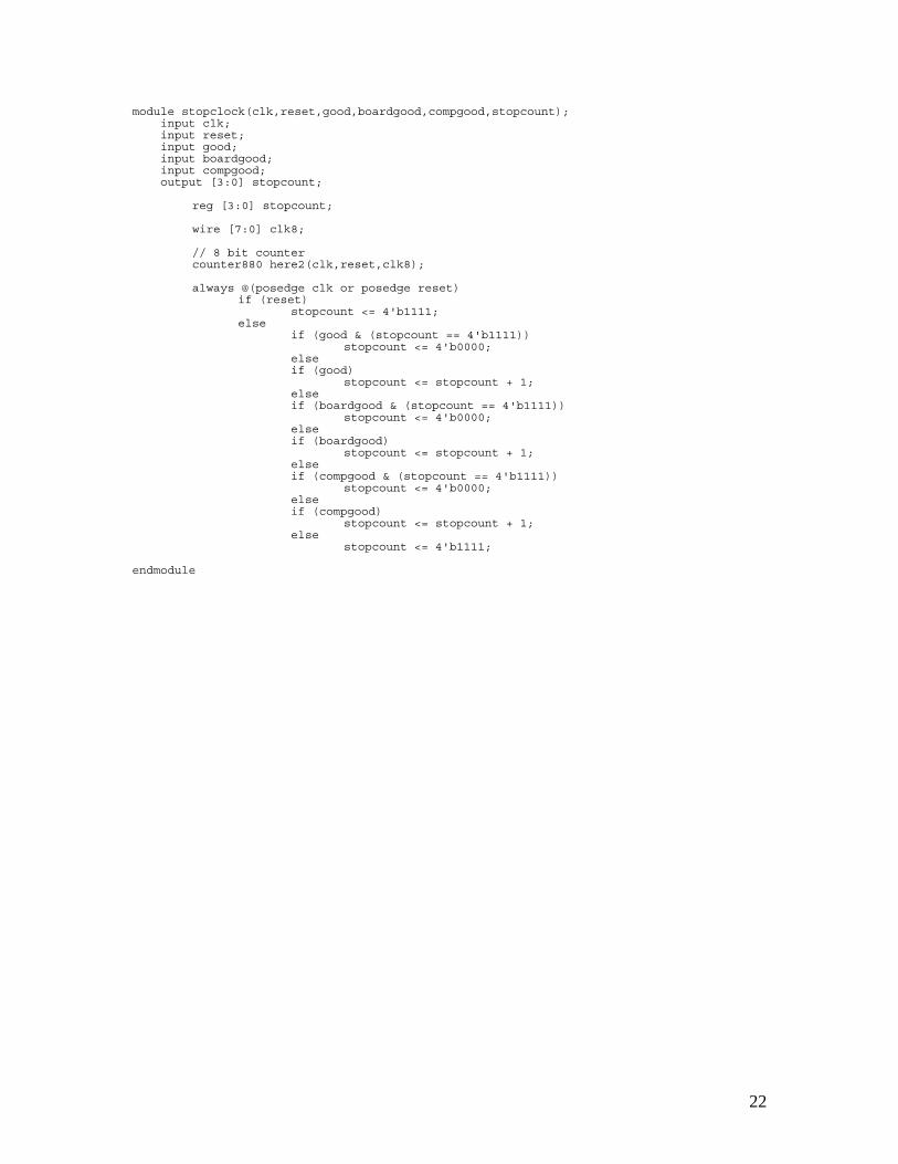
module stopclock(clk,reset,good,boardgood,compgood,stopcount); input clk; input reset; input good; input boardgood; input compgood; output [3:0] stopcount; reg [3:0] stopcount; wire [7:0] clk8; // 8 bit counter counter880 here2(clk,reset,clk8); always @(posedge clk or posedge reset) if (reset) stopcount <= 4'b1111; else if (good & (stopcount == 4'b1111)) stopcount <= 4'b0000; else if (good) stopcount <= stopcount + 1; else if (boardgood & (stopcount == 4'b1111)) stopcount <= 4'b0000; else if (boardgood) stopcount <= stopcount + 1; else if (compgood & (stopcount == 4'b1111)) stopcount <= 4'b0000; else if (compgood) stopcount <= stopcount + 1; else stopcount <= 4'b1111; endmodule
22