Embed Size (px)
Citation preview

JOURNAL OF MICROELECTROMECHANICAL SYSTEMS, VOL. 23, NO. 2, APRIL 2014 259
MEMS Laser Scanners: A ReviewSven T. S. Holmström, Utku Baran, and Hakan Urey, Senior Member, IEEE
Abstract— Laser scanners have been an integral part ofMEMS research for more than three decades. During the lastdecade, miniaturized projection displays and various medical-imaging applications became the main driver for progress inMEMS laser scanners. Portable and truly miniaturized projectorsbecame possible with the availability of red, green, and bluediode lasers during the past few years. Inherent traits of thelaser scanning technology, such as the very large color gamut,scalability to higher resolutions within the same footprint, andcapability of producing an always-in-focus image render it avery viable competitor in mobile projection. Here, we reviewthe requirements on MEMS laser scanners for the demandingdisplay applications, performance levels of the best scanners inthe published literature, and the advantages and disadvantagesof electrostatic, electromagnetic, piezoelectric, and mechanicallycoupled actuation principles. Resonant high-frequency scanners,low-frequency linear scanners, and 2-D scanners are included inthis review. [2013-0235]
Index Terms— Laser displays, MEMS scanners, portableprojectors.
I. INTRODUCTION
S INCE the first scanning silicon mirror was published in1980 [1] microelectromechanical systems (MEMS) for
light scanning has seen a vast array of applications. EarlyMEMS scanners focused on imaging applications such asconfocal microscopy [2]–[7], bar code reading [8], and fingerprint sensing [9]. Around the turn of the new millenniumoptical cross-connects (OXC) technology [10] was the primarydriver for 2D scanners. It has now been supplanted in this roleby the miniaturized projection display with its large demandson frequency, scanning angle, and footprint [11]. Otherapplications include optical coherence spectroscopy (OCT)[12], [13], and the retinal scanning display (RSD) [14],printing [15], head-up displays [16] as well as light detectionand ranging (LIDAR) systems for the automotive industry[17], [18].
For imaging applications, demands on the laser scannerare not as high as in displays. The performance of scannedimaging systems are typically limited by (i) optics, whichdemand small focused spot and dynamic focusing and (ii) lowsignal levels that demand higher integration time and slowscanning speed. Therefore, majority of the highest performing
Manuscript received July 29, 2013; revised December 3, 2013; acceptedDecember 15, 2013. Date of publication January 16, 2014; date of currentversion March 31, 2014. S. Holmström and U. Baran contributed equally tothis paper. Subject Editor O. Solgaard.
S. T. S. Holmström, and H. Urey are with the Department of Electri-cal Engineering, Koç University, Istanbul 34450, Turkey (e-mail: [email protected]; [email protected]).
U. Baran is with the Department of Electrical Engineering, University ofWashington, Seattle, WA 98467 USA (e-mail: [email protected]).
Color versions of one or more of the figures in this paper are availableonline at http://ieeexplore.ieee.org.
Digital Object Identifier 10.1109/JMEMS.2013.2295470
scanners to be discussed in this paper are developed fordisplays, which will be the main focus of this paper.
A. MEMS in Displays
For display applications, there are three types ofarchitectures where MEMS technology have been used:(1) 2-dimensional arrays acting as spatial light mod-ulators (SLM). The most mature technology is TexasInstrument’s Digital light processor (DLP), using Digitalmicromirror devices (DMD) [19], [20], where the MEMScomponent is a large array of bistable micromirrors. Thesedevices have a one-to-one relationship between the num-ber of mirrors and pixel count. (2) Scanned 1-dimensionalarrays, where a 1D array is scanned to generate the full2D image. Two well-known implementations, both usingdiffractive-type optical components, are the grating light valvetechnology (GLV) [21] and the interferometric modulatortechnology (iMoD) [22]. These technologies are today ownedby Silicon Light Machines and Qualcomm, respectively.(3) 2-dimensional laser scanning devices - flying spotdevices - on the other hand, where a single modulated lasersource is scanned simultaneously in two dimensions [23],as detailed in this paper. A comprehensive account of thecompeting MEMS technologies can be found in [24].
B. Lasers in Displays
The first laser displays were proposed already in the 1960’s,but the commercial viability of the technology, especiallyminiaturized implementations, was limited due to bulky andexpensive laser sources [25]. Early examples of compact laserscanners appeared in the late 90s [26]–[29]. The first com-mercially available display system using MEMS-based laserscanning was the RSD, which creates a virtual image directlyonto the eye of the user with laser raster scanning [14]. RSDsystems have existed for over a decade, but more interest isnow directed towards mobile projector displays [30]. However,the development of miniaturized projectors with full color washampered by the bulky frequency doubling schemes that wastypically used as the green laser component [31], [32]. In 2010direct emission green diode lasers became available, enablingcompact red-green-blue (RGB) display engines. This enabledportable and truly miniaturized laser projectors, the beginningof which we are seeing right now.
C. Pico-Projectors
The three currently competitive technologies for miniatur-ized projectors are MEMS laser scanning, DMD, and liquidcrystal on silicon (LCoS) displays [33]. DLP and LCoS areboth examples of SLMs. LCoS is similar to DLP in regardsto working principle, but the reflected light is modulated by
1057-7157 © 2014 IEEE. Personal use is permitted, but republication/redistribution requires IEEE permission.See http://www.ieee.org/publications_standards/publications/rights/index.html for more information.
260 JOURNAL OF MICROELECTROMECHANICAL SYSTEMS, VOL. 23, NO. 2, APRIL 2014
liquid crystals instead of bistable mirrors. The main advantagesof laser scanning are the high color gamut, scalability ofresolution within the same footprint, and an always-in-focusimage [31], [34]. The two latter are especially important forminiaturized displays. Compared to SLM-based systems thedirect modulation of the lasers for each pixel leads to a shiftof architectural complexity from optomechanics to electronics.The direct modulation also facilitates good power efficiencyand inherently high contrast [35]. The major drawback of thelaser scanning approach is laser speckle.
D. Laser Scanners
Traditional techniques for laser scanning include acousto-optic scanners, polygon scanners, and galvanometric scanners.MEMS scanners are desired since they allow miniaturization,low power consumption, as well as much superior performanceat resonant high frequency actuation. A useful and inclusiveclassification of MEMS scanners was formulated in [23]. Witha slightly simplified version of this optical MEMS scannerscan be classified according to the following three categories:(1) operation principle (reflective mirror, refractive lens, anddiffractive grating), (2) actuation principle (mainly electro-static, electromagnetic, piezoelectric, and electrothermal), and(3) fabrication technology (e.g. bulk micromachining, sur-face micromachining, and hybrid fabrication methodologies).However, the vast majority of high performing display scan-ners are torsional mirrors made by silicon bulk micromachin-ing with only actuation method varying.
In this paper the current state of MEMS laser scanners arereviewed and discussed. The main focus is on applicabilityfor miniaturized projectors and wearable displays. It is the firstreview of its kind, but a few earlier reviews have partly treatedthe same topic [11], [36], [37]. Included are comprehensivecomparisons of published scanners and evaluations of thefuture challenges of each technology. Display applicationshave the highest physical demands on the scanner and as theprimary driver of development it is particularly useful to focuson the specific requirements different screen resolution trans-late to. It is the authors’ hope that the information providedcan be of service to everyone planning to design or simplychoose a laser scanner for display as well as various imagingapplications. The aim is to be as inclusive as possible regardingoperation principles, but to focus on the scanner architecturesthat have produced the highest performing scanners.
In Section II scanner requirements and performancemetrics are introduced and discussed. In Section IIIthe commonly utilized actuation principles are compared.In Sections IV, V, and VI published fast scanners, slowscanners, and 2D scanners, respectively, are discussed andcompared. Finally, in section VII the paper is concluded witha discussion on economies of scale, commercialization, and aroadmap for imaging of MEMS scanners.
II. REQUIREMENTS FOR MEMS LASER
SCANNER DISPLAYS
To gauge the performance of a display scanner one needsto consider working frequency, scan angle, mirror size, mirrorflatness (dynamic and static), good mode separation (resonant
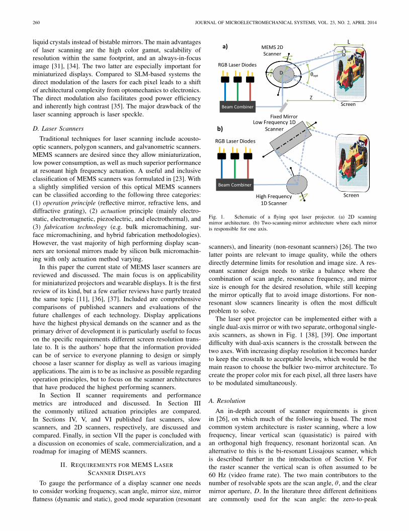
Fig. 1. Schematic of a flying spot laser projector. (a) 2D scanningmirror architecture. (b) Two-scanning-mirror architecture where each mirroris responsible for one axis.
scanners), and linearity (non-resonant scanners) [26]. The twolatter points are relevant to image quality, while the othersdirectly determine limits for resolution and image size. A res-onant scanner design needs to strike a balance where thecombination of scan angle, resonance frequency, and mirrorsize is enough for the desired resolution, while still keepingthe mirror optically flat to avoid image distortions. For non-resonant slow scanners linearity is often the most difficultproblem to solve.
The laser spot projector can be implemented either with asingle dual-axis mirror or with two separate, orthogonal single-axis scanners, as shown in Fig. 1 [38], [39]. One importantdifficulty with dual-axis scanners is the crosstalk between thetwo axes. With increasing display resolution it becomes harderto keep the crosstalk to acceptable levels, which would be themain reason to choose the bulkier two-mirror architecture. Tocreate the proper color mix for each pixel, all three lasers haveto be modulated simultaneously.
A. Resolution
An in-depth account of scanner requirements is givenin [26], on which much of the following is based. The mostcommon system architecture is raster scanning, where a lowfrequency, linear vertical scan (quasistatic) is paired withan orthogonal high frequency, resonant horizontal scan. Analternative to this is the bi-resonant Lissajous scanner, whichis described further in the introduction of Section V. Forthe raster scanner the vertical scan is often assumed to be60 Hz (video frame rate). The two main contributors to thenumber of resolvable spots are the scan angle, θ , and the clearmirror aperture, D. In the literature three different definitionsare commonly used for the scan angle: the zero-to-peak

HOLMSTROM et al.: MEMS LASER SCANNERS: A REVIEW 261
mechanical, θmech , peak-to-peak mechanical, θp−p mech , andfull optical, θopt . For a torsion mirror scanner θopt =2θp−p mech = 4θmech . In this paper θopt is used if not otherwisespecified. Assuming a small angle (paraxial approximation) thenumber of resolvable spots along the horizontal direction (Nh)can be written as
Nh = L
s= 4θmechz
aλ zD
= θopt D
aλ(1)
where, additionally, L is the screen length, s the spot size, z thedistance to the screen λ the longest system wavelength, anda (typically between 0.75 and 2) a shape factor determinedby the definition of spot size (amount of overlap betweenadjacent spots), mirror shape, angle of incidence, fraction ofthe scanline used for writing, and beam profile [26], [40].See the sketch in Fig. 1(a). From (1) it is understood thatthe θopt ·D-product determines the number of resolvable spotsalong the axis. The number of resolvable spots along thevertical axis, Nv, can be calculated from the refresh rate ofthe display (Fr ), the horizontal frequency (fh), the fractionof the time used for retrace of the vertical scanner movingat constant speed (Krt), and the Kub constant which is 1 forunidirectional writing and 2 for bidirectional writing [26].
Nv = fh Kub Krt
Fr(2)
That is, the ratio of horizontal scan frequency to display refreshrate determines the number of vertical lines possible. In thebidirectional writing scheme (Kub = 2) the scanner writestwo lines during one scan cycle, and hence increases the lightsource utilization by a factor of 2 and reduces the requiredhorizontal scanner frequency by half. Although unidirectionalwriting schemes can provide better line to line positionaluniformity, bidirectional schemes are more common and areused for all calculations in this paper [30]. It is also possible tofurther reduce the frequency burden by using multiple beamswith a single mirror. This has been demonstrated [41], butthere are very few implementations and is not consideredfurther in this text. Given a fixed refresh rate (vertical scanningfrequency) each resolution can be translated into fast scannerrequirements expressed as limits of θopt ·D -product and fh .The limit for θopt ·D is set by the horizontal pixel count,while fh is limited by the vertical pixel count. In reverse,they are used as metrics to compare fast scanners. To furtherfacilitate easy comparison of fast scanners operating at dif-ferent frequencies the θopt ·D · f h-product is used as a singlemetric indicating the pixel rate made possible by a specificfast scanner. For requirements on pixel timing we refer to [26].Additional discussion on requirements for linear scanners canbe found in Section V.
B. Dynamic Deformation
For evaluation of a scanner design it is important tounderstand how different features interact with each other.Tradeoffs between scan angle and mirror width with respectto resolution are developed in detail in [14]. For a fixedθopt ·D an increasing D leads to larger mirror deformation,lower maximum frequency, and increasing cost and footprint.
Fig. 2. Sketch of the dynamic mirror deformation.
On the other hand it will provide less tight optomechanicaltolerances and lower flexure stress. For high performance,resonant scanners, the mirror deformation tends to be themost difficult part to solve. High acceleration forces, causedby the mechanical deflection, result in mirror bending, whichin turn leads to optical distortion of the image (Fig. 2).Dynamic deformation of the mirror, defined as the deviationfrom linearity, can be predicted using Brosens’s formula below,which uses the unevenly distributed forces due to accelerationacross the mirror surface,
δmax = 0.217ρ f 2 D5θmech
Et2m
(3)
where, ρ is the material density, E the modulus of elasticity,f the scanner frequency and tm the mirror thickness [6], [42].
To keep the spot diffraction limited, the maximum mechan-ical mirror deformation (δmax) should not exceed λ/10 of theshortest system wavelength [26]. Note that δmax is proportionalto D5. Hence, if the system performance is deformationlimited, significant gains can be attained by slightly reducingthe mirror size. These constraints are the main reason towhy surface micromachining is generally not used for highperformance scanners. In addition to the thicker substrate bulkmicromachining allows for, mirror reinforcement structuresand additional mechanical connections to the mirror framecan also substantially reduce the dynamic deformation. Theearliest studies on well-characterized MEMS mirrors werepublished in 2000 by Urey et al. [26] and Conant et al. [43].Common methods to measure dynamic deformation are mono-chromatic stroboscopic interferometry and stroboscopic whitelight interferometry [26], [44]. Table I shows fh , θopt · D, andmaximum pixel clock frequency requirements for a fast scan-ner needed to address various image resolutions. Bidirectionalraster scanning and 60 Hz refresh rate is assumed. The valuesare calculated based on the equations found in [26]. Exactvalues will always depend on the specific implementation, butthe ones used here are typical and internally consistent.
III. ACTUATION PRINCIPLES
High performance laser display applications require largedisplacements of a large aperture mirror coupled with highmotion precision. Resonant scanners make use of highmechanical quality factor (Q) to reach the required angle. Atatmospheric pressure a very high drive torque is required toovercome the air damping. This problem can be solved by use

262 JOURNAL OF MICROELECTROMECHANICAL SYSTEMS, VOL. 23, NO. 2, APRIL 2014
TABLE I
θ · D AND HORIZONTAL FREQUENCY REQUIREMENTS OF VARIOUS
RESOLUTIONS FOR DISPLAYS USING BIDIRECTIONAL RASTER
SCANNING ARCHITECTURE
TABLE II
COMPARISON OF PROPERTIES OF ACTUATION PRINCIPLES
of a vacuum package, which is costly and leads to a differentset of technical problems [45]. In addition, the suspended massbecomes heavy due to large mirror size and dynamic flatnessrequirements [46]. The non-resonant operation of the verticalscan also demands a high torque to overcome the flexurestiffness that cannot be set very low due to requirements forshock and handling robustness.
The three main actuation principles to be consideredhere are electrostatic actuation (ES), electromagnetic actua-tion (EM), and piezoelectric actuation (PE). Much researchhas also been carried out on electrothermal (ET) scanners[47]–[50]. Due to the inherently long response times of ETdevices, scanners based on this technology is not very suitablefor display applications, but could possibly be used to actuatea slow scanner used in combination with a fast scanner usinga different actuation principle.
When comparing scanners for commercial use, the mostcritical aspects to consider are: enabled resolution, fabricationsimplicity, power efficiency, voltage requirement, robustness,compactness, and long-term stability. Each actuation principlehas advantages in some aspects while having disadvantagesin others. Table II compares qualitatively the properties ofeach actuation principle qualitatively based on the highestperforming scanners designed for miniaturized displays.
A. Electrostatic Actuation
ES actuation was the first actuation method used for MEMSscanners and comprises the vast majority of the publishedliterature. The two main reasons for this are: fabricationcompatibility with any facility with MEMS capability withoutthe need of any unusual material and ease of integration into
Fig. 3. Layout of a ES 2D scanner. The filled trenches are needed for electricisolation. Reprinted with permission from [51].
the full system. In contrast, PE actuators require the depositionof a piezoelectric material while the moving coil EM actuatorsrequire a magnet to be included in the final package.
The working principle of ES actuation relies on the attrac-tion of two oppositely charged plates. The electrostatic forcebetween two plates can be expressed as
Fes = AεV 2
2g2 , (4)
where A is the overlap area of the plates, ε is the dielectricconstant of the medium (i.e. air), V is the voltage differenceapplied between the plates, and g is the gap between the plates.There are two main schemes of electrostatic actuation: combactuation and parallel-plate actuation. Much of the early workmade use of parallel plate actuation, indeed the first siliconscanning mirror published by Petersen in 1980 was of this type[1], [52]. Parallel-plate actuation has great utility for manyapplications with a low θ · D-requirement and is still favouredfor bi-stable mirrors, as in DLP [19]. The basic version ofthe parallel plate actuator is practically very limited in scanrange, since very high actuation voltages are soon requireddue to large electrode separation. On the other hand, combdrive actuation has been the preferred actuation method for EShigh frequency scanners since the turn of the century. In thisscheme multiple plates are attached to each other like combfingers to constitute two interdigitated rows, one static and onefree to move, as illustrated in Fig. 3 [53]. This configurationallows for larger motion and the imparted force to be muchmore evenly distributed over the motion. The first comb fingerdriven micro actuator was described by Tang et al. in 1990,while the first vertical (out-of-plane) comb actuator was madeby Selvakumar et al. in 1995 [54], [55].
ES actuation provides long-term stability, size advantages,and fabrication schemes which are easier to render CMOScompatible. On the other hand, it requires high voltages tooperate, and is sensitive to inexactness in microfabricationdue to the pull-in phenomenon. Particularly comb actuationis prone to fail over large travel ranges due to the interactionof a nonlinear electrostatic force with a linear elastic restoringforce [56]. The pull-in problem is treated in detail in [57]and [58]. This nonlinear leads to a time-varying torsionalstiffness, either named as spring stiffening or spring softening,

HOLMSTROM et al.: MEMS LASER SCANNERS: A REVIEW 263
Fig. 4. Sketch of a typical frequency response of parametric ES scanner.The actuation frequency is typically double the oscillation frequency.
Fig. 5. General configuration of a torsional scanner with coils and magnetsfor a moving coil actuation [61]. To enhance the Lorentz force, more than2 magnets can be used by engineering the positions of the magnets [62].Reprinted with permission from [61].
depending on how the resonance frequency changes withincreasing deflection. The sketch in Fig. 4 shows the typicalfrequency response of a parametric scanner exhibiting ESspring softening. Parametric oscillators can be actuated at2 f /n, where n is a positive integer and f the natural frequency.The deflection is higher for low n. Subsequently, ES scannersare typically actuated at 2f. This is described further in [59]and [60].
B. Electromagnetic Actuation
There are two major EM schemes in use: moving magnetand moving coil. The former uses an external coil togetherwith either a bulk magnet or a thin magnetic film depositedonto the device. It offers simple microfabrication and elim-inates the need of electrical contacts since the actuation isdriven with an off-chip coil. In the moving coil scheme, acoil is fabricated onto a scanner and external magnets areused to provide a static magnetic field, as illustrated in Fig. 5[61], [62]. The configuration makes use of the Lorentz forceacting on the coil when a current is present. Lorentz force,magnetic torque, and the power consumption of the coil canbe calculated as below
FLorent z = Bil, (5)
Tmag = 2∑N
n=1Billrn, (6)
Pcoil = i2rms Rcoil , (7)
where B is the magnetic field, i the current, l the length ofthe conductor, N the number of coil turns, rn the distance ofthe nth coil turn from the center, and R the resistance of thecoil.
Since the actuation force naturally scales with the area,comparative efficiency of EM versus ES actuation increaseswith increasing mirror size [11]. EM actuation also has a morelinear response than the competing principles, rendering it themost suitable for linear slow scanners. However, there arealso drawbacks. The achievable performance of the electro-magnetically actuated MEMS scanner is limited by the largethermal dissipation of the coil. High conducting currents insidea coil also consume significant power, which is a particularlycritical aspect for mobile devices. Additionally, magnets strongenough for high performance take up a significant space andmight require magnetic shielding. This leads to total packagesizes that are larger than the ones for comparable ES and PEscanners.
C. Piezoelectric Actuation
Thin film PE actuation has had somewhat of a late arrivalto MEMS laser scanning due to lack of convenient fabri-cation techniques and machinery, although it provides sev-eral advantages over other methods [63]. As reliable andconvenient fabrication techniques were developed for filmdeposition of piezoelectric materials it has become accepted asa major actuation principle for MEMS scanners during the lastdecade. An alternative to thin filmis the use of stack or bulkpiezoelectric actuators. They are typically bulky and requirehybrid fabrication, which leads to a less streamlined process[15], [64]. On the other hand, they are readily available, low-cost, and can offer high force.
The first attempts to fabricate piezoelectric actuated MEMSused thin film materials such as ZnO and AIN. Lead zirconatetitanate (PZT) is in comparison more cumbersome to deposit,but a film of equal thickness will typically develops tentimes larger force [65]. Hence, PZT is now the most popularmaterial for MEMS scanner actuation. Recently, Hishinumaet al. demonstrated a sputtered PZT film with a piezoelectriccoefficient ∼70% higher than in previously reported sputteredPZT films [66].
The working principle of PZT thin film based actuatorsfor MEMS scanners relies on the stress emanating from theexpansion of the PZT film in x direction when voltage isapplied in the z direction (Fig. 6). Relevant piezoelectriccoefficients for this effect are e31 and d31, which translate thestrain and the stress, respectively, in x direction as a functionof E field in z direction [65]. The corresponding coefficientscan be measured directly by the methods presented in [67].
PE actuation has several distinct advantages. In contrast toEM scanners no magnets or shielding is required, while PEdevices simultaneously operate at a much lower voltage thantypically needed for ES scanners. PE films have a large energydensity and deliver high forces, but a major drawback is theshort stroke length [63], [69]. To reach the relatively largescan angles needed for display scanners some sort of leverageis needed.
264 JOURNAL OF MICROELECTROMECHANICAL SYSTEMS, VOL. 23, NO. 2, APRIL 2014
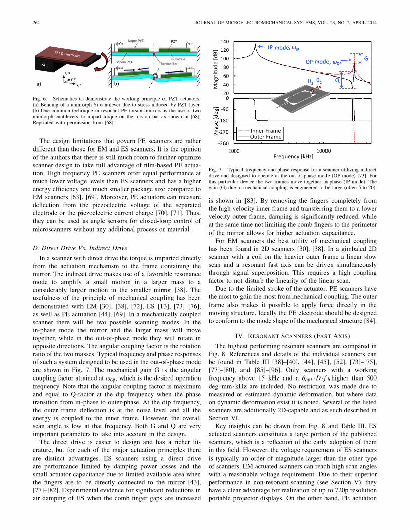
Fig. 6. Schematics to demonstrate the working principle of PZT actuators.(a) Bending of a unimorph Si cantilever due to stress induced by PZT layer.(b) One common technique in resonant PE torsion mirrors is the use of twounimorph cantilevers to impart torque on the torsion bar as shown in [68].Reprinted with permission from [68].
The design limitations that govern PE scanners are ratherdifferent than those for EM and ES scanners. It is the opinionof the authors that there is still much room to further optimizescanner design to take full advantage of film-based PE actua-tion. High frequency PE scanners offer equal performance atmuch lower voltage levels than ES scanners and has a higherenergy efficiency and much smaller package size compared toEM scanners [63], [69]. Moreover, PE actuators can measuredeflection from the piezoelectric voltage of the separatedelectrode or the piezoelectric current charge [70], [71]. Thus,they can be used as angle sensors for closed-loop control ofmicroscanners without any additional process or material.
D. Direct Drive Vs. Indirect Drive
In a scanner with direct drive the torque is imparted directlyfrom the actuation mechanism to the frame containing themirror. The indirect drive makes use of a favorable resonancemode to amplify a small motion in a larger mass to aconsiderably larger motion in the smaller mirror [38]. Theusefulness of the principle of mechanical coupling has beendemonstrated with EM [30], [38], [72], ES [13], [73]–[76],as well as PE actuation [44], [69]. In a mechanically coupledscanner there will be two possible scanning modes. In thein-phase mode the mirror and the larger mass will movetogether, while in the out-of-phase mode they will rotate inopposite directions. The angular coupling factor is the rotationratio of the two masses. Typical frequency and phase responsesof such a system designed to be used in the out-of-phase modeare shown in Fig. 7. The mechanical gain G is the angularcoupling factor attained at ωop, which is the desired operationfrequency. Note that the angular coupling factor is maximumand equal to Q-factor at the dip frequency when the phasetransition from in-phase to outer-phase. At the dip frequency,the outer frame deflection is at the noise level and all theenergy is coupled to the inner frame. However, the overallscan angle is low at that frequency. Both G and Q are veryimportant parameters to take into account in the design.
The direct drive is easier to design and has a richer lit-erature, but for each of the major actuation principles thereare distinct advantages. ES scanners using a direct driveare performance limited by damping power losses and thesmall actuator capacitance due to limited available area whenthe fingers are to be directly connected to the mirror [43],[77]–[82]. Experimental evidence for significant reductions inair damping of ES when the comb finger gaps are increased
Fig. 7. Typical frequency and phase response for a scanner utilizing indirectdrive and designed to operate at the out-of-phase mode (OP-mode) [73]. Forthis particular device the two frames move together in-phase (IP-mode). Thegain (G) due to mechanical coupling is engineered to be large (often 5 to 20).
is shown in [83]. By removing the fingers completely fromthe high velocity inner frame and transferring them to a lowervelocity outer frame, damping is significantly reduced, whileat the same time not limiting the comb fingers to the perimeterof the mirror allows for higher actuation capacitance.
For EM scanners the best utility of mechanical couplinghas been found in 2D scanners [30], [38]. In a gimbaled 2Dscanner with a coil on the heavier outer frame a linear slowscan and a resonant fast axis can be driven simultaneouslythrough signal superposition. This requires a high couplingfactor to not disturb the linearity of the linear scan.
Due to the limited stroke of the actuator, PE scanners havethe most to gain the most from mechanical coupling. The outerframe also makes it possible to apply force directly in themoving structure. Ideally the PE electrode should be designedto conform to the mode shape of the mechanical structure [84].
IV. RESONANT SCANNERS (FAST AXIS)
The highest performing resonant scanners are compared inFig. 8. References and details of the individual scanners canbe found in Table III [38]–[40], [44], [45], [52], [73]–[75],[77]–[80], and [85]–[96]. Only scanners with a workingfrequency above 15 kHz and a θopt ·D · f h higher than 500deg ·mm ·kHz are included. No restriction was made due tomeasured or estimated dynamic deformation, but where dataon dynamic deformation exist it is noted. Several of the listedscanners are additionally 2D-capable and as such described inSection VI.
Key insights can be drawn from Fig. 8 and Table III. ESactuated scanners constitutes a large portion of the publishedscanners, which is a reflection of the early adoption of themin this field. However, the voltage requirement of ES scannersis typically an order of magnitude larger than the other typeof scanners. EM actuated scanners can reach high scan angleswith a reasonable voltage requirement. Due to their superiorperformance in non-resonant scanning (see Section V), theyhave a clear advantage for realization of up to 720p resolutionportable projector displays. On the other hand, PE actuation

HOLMSTROM et al.: MEMS LASER SCANNERS: A REVIEW 265
Fig. 8. Comparison of the highest performing resonant scanners in theliterature working over 15 kHz. The requirements for f and θopt ·D assume60 Hz refresh rate and bidirectional scanning. The dotted lines indicatefh , θopt ·D-levels to give a better understand for how this metric relatesto resolution requirements. See Table III for information on the individualscanners.
is by a large margin the highest performing technology for>30 kHz resonance frequency devices, whereas EM and ESactuations fall short to provide competitive scanners in thisregime. It is reasonable to see indirectly driven PE actuatedscanner as a main candidate for at the least the fast axis inthe next generation high resolution (1080p) displays where∼40 kHz resonance frequency is required.
A. Electrostatically Actuated Scanners
There has been an intense research on ES MEMS scannersfor more than one decade [73], [74], [77], [79], [85], [98]. Thefirst well-characterized high-frequency ES scanner for displayapplications was published in 2000 by Conant et al. [43].It features a 0.55 mm circular mirror resonating at 34 kHzdriven in a direct-drive configuration with staggered verticalcombs (SVC, See Section V-A for more discussion of SVCdevices.). Scanners up to 42 kHz were designed and builtwith the same technology, well beyond what had existedup to that point. Importantly the mirror was dynamicallymeasured and was found to be optically flat. Cho et al.from Samsung Electronics Co. presented a scanner that hasa long SVC actuator attached directly to the mirror [77].Researchers from the same company published in 2006 a fastscanner with an unusual two level SVC actuation [79]. Thedrive consists of combs at three different levels, with staticcomb drives above as well as below the moving combs. Thistype of geometry is otherwise mainly used for quasistaticscanning. Researchers from Fraunhofer Institute for PhotonicMicrosystems (FhG-IPMS) presented a comb actuated mirrorthat meets the strict optical flatness requirement of λ/10 whileproducing optical angle of 40° at the resonance frequency of30.84 kHz [Fig. 9(b)] [87]. Two major measures are made toreduce dynamic deformation. First, the 1 mm mirror plate isattached to a middle frame through 8 joints, which in turnis connected to the substrate with 6 parallel torsion springs.
Fig. 9. Selection of ES scanners. (a) Gimbal-less silicon mirror with threedegrees of freedom (tip-tilt-piston) [97]. Discussed in Section V. Reprintedwith permission from [97]. (b) In this design by Hsu et al. the dynamicdeformation is kept to a minimum by a butterfly shaped reinforcement(not shown) and a complicated suspension structure [87]. Reprinted withpermission from [87]. (c) This scanner by Arslan et al. consists of a mechan-ically coupled system with two cascaded platforms [73]. The mechanicalcoupling is utilized to reach high deflection with relatively small comb fingermotion. (d) SEM of a fabricated 2D microscanner [81]. Reprinted withpermission from [81]. (e) Schematic illustration of the scanners presented byJung et al. [94]. During wafer bonding stamps on the cover wafer are pressingon the deflection pads of the mirror wafer. Through these so called solid bodymechanisms the force is coupled via coupled hinges into vertical deflectionof the comb drive counter electrode. Reprinted with permission from [94].
Second, a butterfly shaped reinforcement structure shapedfrom the handle silicon is left behind the mirror to increaseits stiffness.
In the imaging field much effort has been directed towardsMEMS scanners for miniaturized confocal microscopy, oftenfor endoscopy applications. The starting point was [2] byDickensheets and Kino, where two parallel-plate scannersare used in a monochromatic scanning confocal microscope.A much more recent MEMS-based confocal microscopy isdescribed in [3]. There a single 2D raster scanner carriestwo separated, mechanically conjoined mirrors. One mirroris used for illumination, the other for output collection.To lower the power and avoid the high voltages requiredfor raster scanning, unstable Lissajous scanning was imple-mented for this purpose in [4]. A frame rate of 2 Hz wasaccomplished.
As discussed in detail in Section III-D the indirect driveutilizing mechanical coupling has proven to be very useful forES scanners, since it can decrease damping power losses aswell as it allows for large actuator capacitance. Kurth et al.developed a parallel-plate scanner using indirect drive andshowed an angular coupling ratio as high as 53 [75]. Yoda et al.presented in 2005 the first solution for a comb actuatedscanner [74]. An implementation with higher performancewas published by Arslan et al. [73]. In this 21.8 kHz devicethe mechanically coupled comb drive system consists of twocascaded platforms, the mirror and the comb bearing outerframe [Fig. 9(c)].
B. Electromagnetically Actuated Scanners
Significantly less work has been published on EM resonantscanner compared to ES devices, but it has been clearlyshown that both techniques are competitive and that the chosenactuation principle will depend on the application. For verysmall form factors ES scanners have an advantage. As in the

266 JOURNAL OF MICROELECTROMECHANICAL SYSTEMS, VOL. 23, NO. 2, APRIL 2014
TABLE III
DATA FOR HIGH FREQUENCY SCANNERS FOR THE COMPARISON IN FIG. 8
case of ES scanners, but for slightly different reasons, indirectdrive has proven to be a very important principle, especiallyfor two axis scanners [38]. A majority of the reported highperformance resonant EM MEMS scanners offer 2D scan,which are covered in Section VI-B.
Miyajima et al. presented a large 5 × 3.7 mm2 mirrorwith a rotation of 16.8° optical scan angle in resonance at2.7 kHz [99]. It requires around 350 mA current with Lorentzforce excitation. Raboud et al. reported one of the few 1Delectromagnetically actuated resonant MEMS laser scannersfor microdisplays in the current literature [39]. The 19.5 kHzscanner is planned to be used alongside an EM slow scannerin a VGA capable projection system.
Reyne developed a 20 kHz resonance using moving magnetactuation with a 2 × 4 mm2 mirror that can scan up to5 deg [100]. Yalcinkaya et al. published a moving magnet
2D scanner with an electroplated soft magnetic NiFe layeractuated with an external coil [76]. Actuated at resonancethe slow and fast axes create optical scan angles of 88° and1.8°, respectively. Gokdel et al. presented a 1D soft magneticsteel scanner, where the bulk material also is the actuationmaterial [101]. In [102] Weber et al. describe a process wherenickel is electroplated onto a sacrificial layer, leading to arotating mirror of pure nickel. It is presented as a cheap andsimple alternative. Huang et al. presented a 2D moving magnetscanner using hard magnetic, electroplated CoNiMnP-film.The magnetic material is deposited in stripes to make use ofthe shape anisotropy to increase the efficiency [103]. Anotherexample of the use of hard magnets is described in [104]. Herethe magnets consist of neodymium powder kept in a polymermatrix. A disc of this material is attached directly to the reverseside of the mirror.

HOLMSTROM et al.: MEMS LASER SCANNERS: A REVIEW 267
Fig. 10. Selection of EM scanners. (a) Bi-axial EM drive where the outerframe drives both axes through signal superposition [38], [46]. Reprinted withpermission from [38]. (b) To the left a schematic view of the 2D EM micromir-ror presented in [72]. To the right schematics of the coil and concentric magnetassembly (M: magnetization, F: force, T: torque, H: magnetic field intensity,I: current). Reprinted with permission from [72].
C. Piezoelectrically Actuated Scanners
During the last decade several different actuation configura-tions for PE scanner have been tested. Smits et al. developedone of the first successful piezoelectric thin-film actuatedresonant scanners in 2005, demonstrating 30° at 17.4 kHz [96].The same year Filhol et al. introduced a novel actuator designwith a working frequency of 25.4 kHz in ambient atmosphereconsisting of a silicon membrane and a PZT film [92]. A cir-cular mirror with 500 μm diameter is asymmetrically (50 μmoff axis to the center of mass of the mirror) mounted ontwo lateral torsional hinges linked to the actuators so that thevertical translational excitation is converted into a rotationaloscillatory movement of the mirror. In [106] the rotation isachieved by surrounding the rotation bar with two unimorphactuator beams supplied with opposite voltage. This methodis illustrated in Fig. 6(b).
As already stated Section III-C the major problem toovercome for high angle PE scanners is the limited strokelength of the actuator. Baran et al. proposed a novel actua-tion scheme with a mechanically coupled indirect drive [44].(See Section III-D for more discussion of the indirect drive.)The PZT film is deposited on the outer frame [Fig. 11(b)], sothat the actuation is done within the moving structure itself.The 40 kHz device has an angular coupling ration of 17. Toisolate the mirror and limit the mirror deformation the mirroris suspended by two flexures orthogonal to the torsion bars.This solution is a development of the mirror suspension usedfor the ES scanner presented in [85]. An improved versionof the scanner with approximately 40% performance increasefor corresponding voltage level was presented in [84]. Themechanical structure is identical, but the PZT electrode istailored to have a static deflection profile that conforms withthe desired eigenmode shape. This change decreases the powerwith 23% for a fixed voltage level. At 25V an angle of54.4° is achieved, leading to a θopt · D of 76.3 deg ·mm anda θopt · D · f of 3052 deg ·mm ·kHz. This is the so far the
Fig. 11. Selection of PZT-based PE scanners. (a) The meander-beam solution,here shown to the left, by Tani et al. is the most successful solution for non-resonant PZT scanners so far . The angular displacement is accumulated alongthe turns of the springs. To the right is a 2D scanner combining this methodwith the PE resonant mechanism described in Fig. 6 [68]. Reprinted withpermission from [68]. (b) PZT-driven 40 kHz scanner using mode couplingand a perpendicular mirror hinging [44], [105]. The lower figure shows theshape of the out-of-phase torsion mode. The angular coupling ratio is 17 atthe 39579 Hz resonance frequency. Reprinted with permission from [105].
highest fast scanner performance in the literature. In 2013Gu-Stoppel et al. presented a single-axis scanner actuated withthin-film PZT. The 1 mm mirror scans resonantly ±10.6° at32 kHz [95]. It uses an indirect drive to increase the deflection.This work and the scanner presented by Baran et al. show thatPE scanners in combination with the indirect drive can reachhigher θopt · D · f −numbers than competing technologies.
Metal based piezoelectric scanners have also been investi-gated. Park et al. introduced a stainless steel based piezoelec-tric scanner operating at 28.24 kHz [88]. Moreover, Matsushitaet al. developed a 25.4 kHz PZT film actuated scanner on aTi substrate to simplify the fabrication process of piezoelectricthin film MEMS [91]. Both these metal-based scanners showedgood control of dynamic deformation.
An alternative to PE film is the use of PE bulk elements.Iseki et al. demonstrated a large rotation of ±27° optical scanangle at 38 kHz with 1 mm mirror using a stack piezoelec-tric actuator [89]. In an attempt to get around the materiallimitations of silicon Desai et al. from Cornell Universityproposed in 2006 a hybrid solution where a silicon mirror issuspended by carbon fiber flexures [64]. With the traditionalsilicon flexures replaced by the much more elastic carbonfiber the fatigue limitations eased considerably. The deviceis actuated with an external piezo drive that makes verylarge scan angles possible. Optical angles greater than 180°at 2.5 kHz are reported. What this hybrid technology does notsolve is dynamic deformation of the mirror, which often is themost difficult problem to solve for high frequency scanners.Development of the technology is continued by Mezmeriz Inc.
V. NON-RESONANT SCANNERS (SLOW AXIS)
Polygon and galvanometric scanners with closed-loop con-trol are widely used in various laser-scanning applications

268 JOURNAL OF MICROELECTROMECHANICAL SYSTEMS, VOL. 23, NO. 2, APRIL 2014
and provide an excellent linear scan, but are bulky. Whilemuch research interest has been directed towards resonanthigh frequency scanners, the requirements for the slow axisscanners are at least as difficult to meet. Typical requirementsare 60 Hz operation frequency and a saw tooth scan waveform,capable of constant velocity during the forward scan and fastretrace time for the backward scan. The constant velocityprovides even spacing between the raster lines and the fastretrace time maximizes the fraction of the time used for writingpixels, thus minimizing the frequency requirement for the fastaxis scanner and the display brightness as lasers are turnedoff during the retrace. Since MEMS scanners are suspendedmirrors connected to a frame with torsional flexures, theirdynamic behavior can be modeled as a simple spring, mass,damper system. Under ambient operation conditions, they areunder damped (Q�1) and exhibit resonance behavior. As aresult, the constant speed and fast retrace requirements makeit a challenging design and control problem.
In actual applications the operation frequency of the slowaxis is kept close to the incoming video frame rate (typically60Hz), but not constant. Instead it will be made to varywith the changes in the resonance frequency of the fast axisscanner. There should be an integer ratio between the twoaxis frequencies in a master-slave configuration to produce astationary raster pattern. Due to the large number of harmonicspresent in a saw tooth scan waveform, the slow axis scannerdynamics as well as the changes in the dynamics of both axesdue to temperature shifts need to be taken into account whendesigning the excitation waveform [107].
While raster scanning is the most common approach, socalled Lissajous scanning with two resonant axes has alsobeen demonstrated. The main advantages with this approachcome with the driving requirements for the slow axis dueto absence of harmonics [45], [51], [108]. The power con-sumption is also somewhat smaller. On the negative side, theraster lines are not evenly spaced and correcting this leadsto complicated electronics and an increase of the requiredhorizontal frequency. Even when this requirement is fulfilledthe resulting refresh rate is lower than for a comparable rasterscanning system. Bi-resonant actuation also demands largerelectronic bandwidth. For the best coverage in a Lissajoussystem a high ratio between the two resonant axes is desired.This requires the slow scanner to work resonantly at verylow frequencies, which makes the system very fragile andsensitive to vibrations. In [45] this is addressed by a proposedsetup where two fast scanners are paired. The two axes areindividually monitored by phase-locked loop circuitry (PLL)to keep the difference between the two working frequencies atexactly 60 Hz. In this way you get a rather robust system, butone that is not aiming at high end applications. The commonassumption in the literature is that Lissajous scanners are notwell-suited for high quality displays, but probably more so forimaging applications where a feedback signal together withdata processing can reconstruct the a high resolution image.There are examples of successful use of Lissajous scannersin endoscopic and confocal microscopy applications [4]. Formore in-depth discussions of Lissajous scanning the authorsrefer to the following references [45], [109]–[111].
TABLE IV
HIGH PERFORMING NON-RESONANT SCANNERS. AVC: ANGULAR
VERTICAL COMBS. SVC: STAGGERED VERTICAL COMBS
Only a few quasistatic scanners with high θopt are found inthe literature, but is has been well demonstrated that this can bedone for ES [94], [112], [113] and EM [38], [114] scanners.For PE scanners some very good progress has been made,but more work remains to be done [68]. In this section non-resonant 1D scanners are mainly discussed, see Section VI forthose included in 2D scanners. For a better overview some ofthe highest performing non-resonant scanners in the literatureare collected in Table IV.
A. Electrostatically Actuated Scanners
To facilitate quasistatic ES scanning it is necessary tohave a vertical separation (off-set) between the moving andstatic electrodes. For comb drive actuators the two mostimportant approaches are staggered vertical combs (SVC) andthe angular vertical combs (AVC). The earliest SVC scannerused partial polysilicon refill of vertical trenches to formthe comb fingers [55]. The straightforward way to fabricatethese nowadays is to form the two finger sets in separatedevice layers in an SOI wafer [43], [112]. Two drawbacksshared by most SVC fabrication schemes are the complicatedfabrication schemes and the fact that the static and movingfinger sets are defined with separate mask, leading to very strictalignment requirements. To address the latter point severalmethods to fabricate so called self-aligned comb drives, whereall fingers are defined with one mask, have been developed[113], [115], [116]. However, these solutions increase thecomplexity even more. In their 2004 paper Milanovic et al.presented a scanner where timed etches are used to createall comb sets from the same silicon layer [97]. They reporta gimbal-less micromirror [Fig. 9(a)] actuated by three orfour vertical comb drive rotators. These rotators are coupledthrough mechanical rotation transformers to a central mirror.The one-axis micromirror is capable of angles above ±5°when operated below 150 V operation. Devices with threeor four rotators have three degrees of freedom (tip-tilt-piston).In 2002 Milanovic demonstrated a scanner with an SOI-basedfabrication schedule with an optical angle of ±19.5° [112].Carlen et al. presented several SVC devices with ±10° opticalangle [113].
HOLMSTROM et al.: MEMS LASER SCANNERS: A REVIEW 269
In AVC devices static and moving fingers are typicallydefined in one layer with one mask. This removes much ofthe fabrication complexity of SVC devices. In the next stepa static offset angle is created. Many techniques have beenpresented to achieve this offset, among them are stress inducedbending in multilayered joints [117], surface-tension forcesfrom reflow of photoresist [118], or plastic deformation ofsilicon through annealing [119]. It has also been shown AVCactuators are more efficient than SVC for the same fingergeometry [118].
Researchers at Fraunhofer IPMS (FhG-IPMS) presentedscanners with out-of-plane combs constructed by deformingin-plane combs during a wafer bonding step between themirror wafer and a cover wafer [94]. During the bonding stepso called solid body mechanisms on the scanner wafers aredeflected by stamp structures on the cover wafer [Fig. 9(e)].Both AVC and SVC structures are fabricated with this tech-nique. The main difficulty with this fabrication scheme isto reach the acquired lateral resolution in the wafer bondingstep. The authors report a maximum lateral displacement of±0.6 μm. See also Section VI-A.
As an alternative, in-plane rotation using curved combfingers can also be used to drive scanning platforms for laserscanning applications. In [120] such a mechanism was used torotate a 1 mm in-plane grating for monochrome scanning up to25° at resonance. One problem with in-plane MEMS scannersusing tether suspensions is the nonlinear spring stiffening ofsuspension beams used in bending mode rather than torsionmode [121]. An ES rotating platform utilizing a suspensiongeometry designed to provide a linear ramp motion with avertically mounted mirror was demonstrated in [53].
B. Electromagnetically Actuated Scanners
There are several successful examples of electromagnet-ically actuated non-resonant MEMS laser scanners. Lessnonlinear drive and longer operation range capabilities ofEM actuators make them suitable for quasistatic operation.Jeong et al. from Samsung Electrics Company, Ltd. proposeda Lorentz force slow scanner that can be used to horizontallyscan a vertical line image made through a line-type diffractiveSLM [122]. In this design a large 3 × 1.5 mm2 mirroris rotated quasistatically up to ±15° with 98% linearity at120 Hz, while consuming 60 mW. To minimize the devicesize and the power consumption the coil actuator is placeddirectly on the reverse of the mirror. Moreover, mechanicalstoppers are used to make the device shock-proof. Wafer-levelpackaging is realized using an additional glass wafer, and totalsize of the package is 9.2 mm × 10 mm × 3 mm (0.28cc).
Moreover, Makishi et al. uses moving magnet actuationto generate very large mirror rotations up to ±59° opticalangle [114]. Four permanent magnets are attached to a double-gimbal structure and the mirror rotation is realized with fourelectromagnets. The possible unreported problems with thisdevice are large size due to the bulky electromagnets and poorshock resistance. Permanent magnets add comparably largeamount of inertia to the double-gimbal structure and makes iteasier to break under shock.
Ataman et al. presented a non-gimbaled 2D moving magnetpointing mirror for use with high power lasers [18]. Themirror is suspended by 25 hidden and radially symmetrics-shaped beams. A magnet is attached to the mirror belowthe pivot point. The mirror can be mechanically tilted ±4°(±8° optical) along both axes by current applied to two coils,stacked beneath the mirror.
C. Piezoelectrically Actuated Scanners
The limited displacement of piezoelectric actuation is amajor problem for non-resonant MEMS scanners. Hence,there are few examples of non-resonant MEMS scanners withpiezoelectric actuation in literature. Tani et al. introduced asolution to overcome the limited deflection of piezoelectricallyactuated beams [68], [123]. In this design large quasistaticallyactuated angles up to ±17.2° are achieved at an appliedvoltage of 20 Vdc by accumulating angular displacement in ameandering piezoelectric cantilever, as illustrated in Fig. 11(a).Kobayashi et al. used meandering cantilevers to create large,non-resonant angle rotation of a mirror [124]. In this way,±10.6° at an applied voltage of 10 Vdc is achieved.
Meandering type cantilevers are known to have a problemwith an abundance of parasitic modes at the typically desiredlow frequencies, making it a challenge to achieve linearscanning that is pure enough for high performance displays.The approach suggested by Tani et al. for quasistatic PEscanning is, however, clearly the most promising so far, butmuch work on detailed mode design will probably be requiredto get this type of scanner to work with the precision needed.
VI. 2D SCANNERS
The first silicon 2D MEMS scanner was published alreadyin 1994 by Asada et al. [125]. Most high performance dual axisscanners for display applications use a gimbaled torsion mech-anism. However, several gimbal-less approaches have beendemonstrated. Scanners with the actuation mechanics hiddenbeneath the mirror are especially important for applicationsthat require very small die size or high mirror fill-factor [18],[48], [126]. A non-gimbal approach was also used in the tip-tilt-piston mirror presented by Milanovic et al. [97].
A few hybrid approaches to 2D scanning have been pub-lished. Already a decade ago Microvision made an ES/EM 2Dscanner. The device required a vacuum package and utilizedEM actuation for a slow raster scan and ES parallel platedrive for resonant fast scanning [30]. A distinct possibility forhybrid 2D scanners is ET actuation. Successful 2D scanningET micromirrors have been presented [48], but it is inherentto the actuation principle that the reaction times are too longto be used for the fast axis in a display. To function for thispurpose a slow ET actuator would need to be paired with adifferent actuation scheme for the fast axis. 2D ET scannersusing ES and EM, respectively, for the fast axis have beenreported [49], [50], but it remains to be proven if it is a viableidea or not.
A. Electrostatically Actuated Scanners
The 2D ES microscanner is a very good candidate forminiaturized laser projectors, the main drawback being the
270 JOURNAL OF MICROELECTROMECHANICAL SYSTEMS, VOL. 23, NO. 2, APRIL 2014
high voltage requirements typically needed. FhG-IPMS hasbeen developing electrostatically actuated MEMS scanners forover a decade [87], [127]. Much of the work has been on 2Dscanners for microdisplays utilizing Lissajous scanning (seeSection II and the introduction of V) [51], [94], [108]. In 2008they presented the first 2D ES scanner capable of SVGA reso-lution [108]. The gimbaled scanner uses a fast axis frequencyof 30 kHz and a slow axis of either 70Hz or 330Hz. The designof the fast axis is the same as in [87], previously discussed inSection IV-A. The dynamic deformation is established to bewithin the optical requirements. The high frequency of the fastaxis is needed for SVGA because of the Lissajous scheme. Therequired frequency for the corresponding raster scanner wouldbe around 20 kHz. In 2011 researchers at FhG-IPMS presentednewly developed dual-axis micromirrors capable of performinghigh frequency resonant scanning as well as linear quasistaticscanning [94]. For the quasistatic slow axis both SVC andAVC configurations are been realized (see Section V-A). Thefast axis scans up to ±19° at 23.3 kHz, while the presentedquasistatic axes give optical scan angles up to ±15°. The 2Dscanners have mirrors with 1.2 mm in diameter. Pure slowscanners with mirror diameter of 4 mm are also presented.
Hofmann et al. reported several ultra-high Q 2D scanners forLissajous operation in vacuum [45]. One of the four presenteddesigns reaches ±43° at 30.8 kHz. The approach used is tolower the voltage requirements for high performance scannersby way of very high Q of 145,000 for the slow axis and60,000 for the fast axis. To achieve this wafer level vacuumpackaging is used. With a 0.8 mm mirror this gives aθO PT ·D = 68.8 deg ·mm and a θO PT · D · f =2119 deg ·mm ·kHz. The power consumption is below1 mW with both axes running. These are the highestperformance metrics for an ES fast scanner to date. Whenoperating in ambient atmosphere the scan angle is aboutone tenth of these values. The drawbacks with the highQ are extremely long amplitude decay times (minutes),high sensitivity of the resonance frequency to temperaturechanges, and when both axes have extremely high Q thesynchronisation of them becomes very difficult.
Chu et al. reported two bi-resonant, gimbaled 2-D combdrive scanners, using direct drive for both axes [Fig. 9(d)][81]. One of the scanners exhibit resonant frequencies for theinner mirrors and the gimbal frame of 40 kHz and 162 Hz,respectively. The maximum scan angle for the fast axis is±10.8° operating at 1 Pa. At ambient pressure the performanceis limited. Researchers from the Adriatic Research Institutepresented in [128] a projection systems based on their non-gimbaled 2D scanners [97], described in Section V-A. Themirror can rotate mechanically up to ±4° on each axis, butwith an added fisheye lens the optical angle can reach 120°.Both axes can be actuated linearly at arbitrary frequencies upto 4 kHz, making it especially suitable for vector displays.
B. Electromagnetically Actuated Scanners
2D EM laser scanners are core components of commerciallyavailable mobile projectors [30], [39]. Microvision Inc. hasbeen utilizing Lorentz force excited 2D MEMS scanners as
an engine for their NOMAD head-worn displays and PicoPmobile projectors [30], [38], [46]. Early designs required avacuum package, significantly increasing size and cost. In2005 this approach was replaced by a new bi-axial magneticdrive scheme to be used in ambient atmosphere [46]. Thescheme was detailed in 2006 by Yalcinkaya et al. and thefeatured scanner was the first SVGA capable 2D raster scanner,see Fig. 10(a) [38]. The 1.5 mm mirror gives optical angles upto ±26.5° and ±33.5° at resonant horizontal scan at 21.3 kHzand non-resonant vertical scan at 60 Hz, respectively. Thescanner utilizes Lorentz force actuation. For actuation thedevice is placed in an external magnetic field, at a 45° angle,allowing both modes to be actuated simultaneously by superpositioning of two driving signals in the coil covering thegimbal frame. For the resonant scan the out-of-phase modeis used to benefit from mechanical coupling.
An interesting addition to the literature on Lorentz scannerswas presented by Sung et al. in [129]. The authors note that ina traditional Lorentz scanner like the one by Yalcinkaya et al.where the coil is deposited on the silicon surface there will be aslight asymmetry in the actuation, leading to a wobble motion.In this work the wobble motion is minimized by the use of aSi-Ni compound frame, where the Ni coil spans through thefull thickness of the scanner.
Ji et al. presented a scanner that again uses the mechanicalcoupling principle for resonant scanning, but it utilizes a singleturn coil and radial magnetic field from concentric magnetassembly rather than using a multi turn coil and a lateral mag-netic field oriented 45° to the scan axes to achieve a bi-axialmagnetic actuation, see Fig. 10(b) [72]. A single turn coil iseasier to fabricate than a multi turn coil. A concentric magnetassembly, composed of cylindrical and annular magnets andan iron yoke, provides larger radial magnetic field comparedagainst the conventional magnets. In this design, 1.5 mmmirror operating with 131 mA current produces 8.8° and 8.3°optical scan angles in resonance operation at 19.1 kHz, and instatic mode operation at 60 Hz, respectively.
C. Piezoelectrically Actuated Scanners
While there have been several examples of biresonant PE2D scanners, it has proven to be very difficult to design ahigh performance dual-axis scanner for raster scanning [93],[106], [130]. Chen et al. presented in 2012 a 2D Lissajousscanner driven by an external PZT unit [93]. The resonancefrequencies of axes are 25 kHz and 560 Hz, respectively andprojects images with a 640 × 480 resolution. Gu-Stoppel et al.presented a gimbal-less stage with three degrees of freedomgranted by four PZT-clad cantilevers [131]. The torsion modesresonate at 28.6 kHz and the piston mode at 21 kHz.
The meander spring presented by Tani et al. is describedabove in Section V-C. These springs can be actuated eitherquasistatically or at resonance. A scanner using the meanderspring for both axes was presented in [123]. Non-resonantoptical angles of ±17.2° and ±11.2° were found for the outerand inner axes, respectively. Separately, a hybrid scanner wascreated where a meandering slow outer axis is combined with amore traditional torsion beam twisted by two unimorph beams

HOLMSTROM et al.: MEMS LASER SCANNERS: A REVIEW 271
for a fast inner axis [68]. The scanner is shown in Fig. 11(a). Inthis work, 2D scan is demonstrated with a resonant operationat 11.2 kHz for the fast horizontal axis with 39° optical angleand quasistatic operation at 60 Hz of the slow vertical axiswith ±7.25° while operated at 40 Vpp. With that it is the firstsuccessful demonstration of a piezoelectrically actuated rasterscanner in the literature.
VII. DISCUSSION AND CONCLUSION
A. Fabrication and Packaging
The processes of MEMS fabrication are derived from thevery mature semiconductor IC industry. While the MEMSfield still lack standardization compared to the IC industry,the MEMS industry is maturing rapidly with greater standard-ization as one inevitable result. We have already seen thickSOI based wafers with device layer thickness in the rangeof 30 μm to 150 μm becoming the standard substrate forscanners, leading to simple and robust structures. As shownin Fig. 8, all three actuation principles reviewed in this papercan produce high performance scanners. One disadvantage formagnetically actuated scanners is the cost and volume taken upby the required magnets. They also require good shielding formagnetic interference. From a manufacturing point-of-view, allthree types can use standard materials and fabrication methods.While some of the early MEMS scanners exploited the use ofexpensive vacuum packaging, of more recently reported high-performance scanners most operate at ambient pressure anddo not have special packaging requirements.
B. Economies of Scale
The die area primarily determines the cost of the scannersin high volume production. Increasing the resolution by wayof increasing the scan angle does not increase the scanner costand allows scalability to higher resolutions. While the scannercost is important, the cost of the system is dominated by thelasers not by the scanners in display and imaging devices.Power consumption per scan axis can be less than 100 mWfor all types of scanners. While the power consumption of EMactuated scanners is higher, the system power consumption isdominated by the lasers and the video electronics rather thanby the scanners.
C. Technology Comparison for Miniaturized Displays
For microdisplay applications, major competitors to laserscanning are DLP and LCOS based systems that use LEDs aslight source. Key advantages of the laser scanners for mobileprojection displays are in the scaling to higher resolutions andfocus-free operation without requiring a projection lens. Froman economic perspective chips for laser scanning are simpler tofabricate and smaller in die area, thus cost less. One drawbackof the laser-based systems is speckle, which degrades theimage quality. However, there are various methods to reducethe speckle contrast to acceptable levels in laser displays [31].Both LED and laser based mobile displays are currentlylimited in brightness due to eye safety and battery powerlimitations. However, novel screen designs with high-gain
can offer high-efficiency, high-brightness and a new foundflexibility for 2D and 3D projection displays [132], [133].
D. Commercialization trends for displays
The field has already reached some maturity and there arealready commercial offerings with a wide variety of technicalsolutions for high performance MEMS laser scanners. Thefirst product in the market was Microvision NOMAD in 2004,which used a 2D scanner with parallel-plate ES scanner for fastaxis and moving coil EM scanner for slow axis. Later productsof Microvision used 2D EM scanners and more recentlyLemoptix SA and Nippon Signal also offer both 1D and 2DEM scanners. Fraunhofer IPMS (and its spin-off HyperscanGmbH), Mirrorcle Technologies, and Opus Microsystems (1Dand 2D ES) have been offering 1D and 2D ES scanners .There are also some more unusual approaches such as the2D scanner from Maradin Ltd. with an ES fast scanner andmoving magnet slow scanner and the hybrid PE solutionfrom Mezmeriz Inc (see Section IV-C for more detail of thelatter). There are other companies such as Stanley and BTendo(acquired by STMicroelectronics) who developed scanners forcommercialization but details are not available.
E. Roadmap for Medical Imaging Applications
There is much interest for miniaturized imaging solutionsbased on laser scanning in the medical field. The speed andthe resolution of the camera based systems are typically deter-mined by camera refresh rate and light source/optics while thescanning based systems are often limited by the low signallevels collected from the samples, which limit the bandwidthof detection and the scanning speed. Additional requirementsin medical imaging applications are micron level small spotsize, large field-of-view (or scan angle), and dynamic focusingdue to limited depth-of-focus, which present major challengesin the optical design. For the scanning unit, <2 kHz scanningfrequency for the fast axis and a high precision ramp scanningin the slow axis are preferred. Galvo scanners have beendominating the scanner market for imaging applications dueto their superior linearity and stability up to 1 kHz scanningfrequency. However, the efforts for miniaturizing the scanningunit, especially for endoscopic applications, generated a sub-stantial literature about MEMS scanners for imaging appli-cations. The performance requirements on MEMS scannersfor imaging applications typically are much lower in termsof frequency and scan angle compared to those of in thedisplay field and the challenges are more related to packaging.Good summaries of these scanners can be found in [134]and [135]. The main challenges for MEMS scanners developedfor endoscopic imaging applications are compact package sizerequirement (preferably <10 mm3), poor image quality (dueto aberrations from scanning mirror and objective lens), andstability. These challenges have to be overcome to enable theimplementation of MEMS scanners into commercial imagingsystems. EM actuators fail to deliver compact package size dueto their need for a bulky magnet. On the other hand, ES andPE actuated MEMS scanners are closer candidates to satisfythe requirements of endoscopic imaging applications, however

272 JOURNAL OF MICROELECTROMECHANICAL SYSTEMS, VOL. 23, NO. 2, APRIL 2014
significant engineering effort is still needed to limit opticalaberrations and to control scanner stability.
In conclusion, we can assert that MEMS laser scanner baseddisplay and imaging systems offer several clear advantagesand expected to have a bright future particularly in mobileconsumer displays and medical imaging devices.
ACKNOWLEDGMENT
The authors would like to thank Microvision Inc. for ourlongstanding collaboration, special thanks to Dean Brown,Wyatt Davis, Mark Helsel, and Randy Sprague for countlessfruitful discussions on these topics. For help with technologydevelopment the authors would also like to thank Paul Muraltand Davide Balma from École Polytechnique Fédérale deLausanne and Harald Schenk from Fraunhofer IPMS. Alsomany thanks to present and former colleagues at OML: ArdaYalcinkaya, Caglar Ataman, Aslihan Arslan, Sertan KutalGokce, Selim Olcer, Basarbatu Can, and Ugur Aygun.
REFERENCES
[1] K. E. Petersen, “Silicon torsional scanning mirror,” IBM J. Res.Develop., vol. 24, no. 5, pp. 631–637, 1980.
[2] D. Dickensheets and G. Kino, “Micromachined scanning confocaloptical microscope,” Opt. Lett., vol. 21, no. 10, pp. 764–766, May 1996.
[3] W. Piyawattanametha, H. Ra, M. J. Mandella, K. Loewke, T. D. Wang,G. S. Kino, et al., “3-D near-infrared fluorescence imaging using anMEMS-based miniature dual-axis confocal microscope,” IEEE J. Sel.Topics Quantum Electron., vol. 15, no. 5, pp. 1344–1350, Sep. 2009.
[4] J. T. C. Liu, N. O. Loewke, H. Ra, O. Solgaard, C. H. Contag,G. S. Kino, et al., “Micromirror-scanned dual-axis confocal microscopeutilizing a gradient-index relay lens for image guidance during brainsurgery,” J. Biomed. Opt., vol. 15, no. 2, pp. 026029-1–026029-5, 2010.
[5] K. H. Gilchrist, D. E. Dausch, and S. Grego, “Electromechanicalperformance of piezoelectric scanning mirrors for medical endoscopy,”Sens. Actuators A, Phys., vol. 178, pp. 193–201, Apr. 2012.
[6] D. L. Dickensheets, “A microfabricated scanning confocal opticalmicroscope for in situ imaging,” Ph.D. dissertation, Dept. Elect. Eng.,Stanford Univ., Stanford, CA, USA, 1998.
[7] D. L. Dickensheets and G. S. Kino, “Silicon-micromachined scanningconfocal optical microscope,” J. Microelectromech. Syst., vol. 7, no. 1,pp. 38–47, Mar. 1998.
[8] S. O. Isikman, R. B. Sprague, and H. Urey, “FR4 laser scannerwith dynamic focus,” IEEE Photon. Technol. Lett., vol. 21, no. 4,pp. 233–235, Feb. 15, 2009.
[9] A. P. Neukermans and T. G. Slater, “Micromachined torsional scanner,”U.S. Patent 5 629 790, May 13, 1997.
[10] V. A. Aksyuk, F. Pardo, C. A. Bolle, S. Arney, C. R. Giles, andD. J. Bishop, “Lucent microstar micromirror array technology for largeoptical crossconnects,” Proc. SPIE, vol. 4178, pp. 320–324, Aug. 2000.
[11] P. R. Patterson, D. Hah, M. Fujino, W. Piyawattanametha, andM. C. Wu, “Scanning micromirrors: An overview,” Proc. SPIE,vol. 5604, pp. 195–207, Oct. 2004.
[12] Y. Pan, H. Xie, and G. K. Fedder, “Endoscopic optical coherencetomography based on a microelectromechanical mirror,” Opt. Lett.,vol. 26, no. 24, pp. 1966–1968, Dec. 2001.
[13] K. Isamoto, K. Totsuka, T. Suzuki, T. Sakai, A. Morosawa, C. Chong,et al., “A high speed MEMS scanner for 140-kHz SS-OCT,” in Proc.IEEE Opt. MEMS, Istanbul, Turkey, Aug. 2011, pp. 73–74.
[14] H. Urey, D. W. Wine, and J. R. Lewis, “Scanner design and resolutiontradeoffs for miniature scanning displays,” Proc. SPIE, vol. 3636,pp. 60–68, Apr. 1999.
[15] W. O. Davis, D. Brown, M. Helsel, R. Sprague, G. Gibson,A. Yalcinkaya, et al., “High-performance silicon scanning mirrorfor laser printing,” Proc. SPIE, vol. 6466, pp. 64660D-1–64660D-7,Jan. 2007.
[16] M. K. Hedili, M. O. Freeman, and H. Urey, “Microstructured head-up display screen for automotive applications,” Proc. SPIE, vol. 8428,pp. 84280X-1–84280X-6, Jun. 2012.
[17] U. Hofmann, F. Senger, F. Soerensen, V. Stenchly, B. Jensen, andJ. Janes, “Biaxial resonant 7 mm-MEMS mirror for automotive LIDARapplication,” in Proc. Int. Conf. Opt. MEMS Nanophoton., Banff, AB,Canada, 2012, pp. 150–151.
[18] Ç. Ataman, S. Lani, W. Noell, and N. de Rooij, “A dual-axis pointingmirror with moving-magnet actuation,” J. Microelectromech. Syst.,vol. 23, no. 2, p. 025002, Dec. 2012.
[19] L. J. Hornbeck, “The DMD projection display chip: A MEMS-basedtechnology,” MRS Bull., vol. 26, no. 4, pp. 325–327, Apr. 2001.
[20] S. C. Shin, Y. Jung, T. J. Ahn, S. S. Jeong, S. G. Lee, and K. Y. Choi,“The compact systems design based on DMD and the straight line2-channel LED for a mobile embedded pico projector,” J. DisplayTechnol., vol. 8, no. 4, pp. 219–224, Apr. 2012.
[21] O. Solgaard, F. Sandejas, and D. Bloom, “Deformable grating opticalmodulator,” Opt. Lett., vol. 17, no. 9, pp. 688–690, May 1992.
[22] A. Londergan, E. Gousev, and C. Chui, “Advanced processes forMEMS-based displays,” in Proc. Asia Displays, Shanghai, China, 2007,pp. 107–112.
[23] T. Bourouina, H. Fujita, G. Reyne, and M. E. Motamedi, “Optical scan-ning,” in Micro-Opto-Electro-Mechanical Systems, M. E. Motamedi,Ed. Bellingham, WA, USA: SPIE, 2005, pp. 323–367.
[24] H. Urey, S. Madhavan, and M. Brown, “MEMS microdisplays,” inHandbook of Visual Display Technology, J. Chen, W. Cranton, andM. Fihn, Eds. Bristol, U.K.: Springer-Verlag, 2012, pp. 2067–2080.
[25] A. Korpel, R. Adler, P. Desmares, and W. Watson, “A television displayusing acoustic deflection and modulation of coherent light,” Appl. Opt.,vol. 5, no. 10, pp. 1667–1675, Oct. 1966.
[26] H. Urey, D. W. Wine, and T. D. Osborn, “Optical performancerequirements for MEMS-scanner based microdisplays,” Proc. SPIE,vol. 4178, pp. 176–185, Aug. 2000.
[27] K. Yamada and T. Kuriyama, “A novel asymmetric silicon micro-mirrorfor optical beam scanning display,” in Proc. 11th Annu. IEEE MicroElectro Mech. Syst., Kanagawa, Japan, Jan. 1998, pp. 110–115.
[28] R. A. Conant, P. M. Hagelin, U. Krishnamoorthy, M. Hart, O. Solgaard,K. Y. Lau, et al., “A raster-scanning full-motion video display usingpolysilicon micromachined mirrors,” Sens. Actuators A, Phys., vol. 83,pp. 291–296, May 2000.
[29] H. Schenk, “A novel micro actuator for one and two dimensionaldeflection of light,” Ph.D. dissertation, Dept. Elect. Eng., GerhardMercator Univ., Duisburg, Germany, 2000.
[30] J. Tauscher, W. O. Davis, D. Brown, M. Ellis, Y. Ma, M. E. Sherwood,et al., “Evolution of MEMS scanning mirrors for laser projec-tion in compact consumer electronics,” Proc. SPIE, vol. 7594,pp. 75940A-1–75940A-12, Feb. 2010.
[31] K. V. Chellappan, E. Erden, and H. Urey, “Laser-based displays:A review,” Appl. Opt., vol. 49, no. 25, pp. F79–F98, Sep. 2010.
[32] Y. Hirano, S. Yamamoto, Y. Akino, A. Nakamura, T. Yagi, H. Sugiura,et al., “High performance micro green laser for laser TV,” in Proc.Adv. Solid-State Photon., Denver, CO, USA, 2009, pp. 1–3.
[33] S. J. Park, S. M. Kim, and C. S. Won, “Design considerations forpico-projector based on LCoS and 3-LEDs,” in Proc. IEEE ConsumerElectron., Las Vegas, NV, USA, Jan. 2011, pp. 805–806.
[34] W. O. Davis, M. Beard, and R. Jackson, “Trajectory precision of micro-machined scanning mirrors for laser beam scanning pico-projectordisplays,” Proc. SPIE, vol. 8252, pp. 825203-1–825203-11, Mar. 2012.
[35] M. Freeman, M. Champion, and S. Madhavan, “Scanned laser pico-projectors: Seeing the big picture (with a small device),” Opt. Photon.News, vol. 20, no. 5, pp. 28–34, May 2009.
[36] C. Liao and J. Tsai, “The evolution of MEMS displays,” IEEE Trans.Ind. Electron., vol. 56, no. 4, pp. 1057–1065, Apr. 2009.
[37] M. C. Wu, O. Solgaard, and J. E. Ford, “Optical MEMS for lightwavecommunication,” J. Lightw. Technol., vol. 24, no. 12, pp. 4433–4454,Jan. 2006.
[38] A. D. Yalcinkaya, H. Urey, D. Brown, T. Montague, and R. Sprague,“Two-axis electromagnetic microscanner for high resolution displays,”J. Microelectromech. Syst., vol. 15, no. 4, pp. 786–794, Aug. 2006.
[39] D. Raboud, T. Barrasa, F. Lo Contea, L. Fabrea, L. Kilcherb,F. Kechanab, et al., “MEMS based color-VGA micro-projector system,”Proc. Eng., vol. 5, pp. 260–263, Sep. 2010.
[40] H. Urey, “Torsional MEMS scanner design for high-resolution displaysystems,” Proc. SPIE, vol. 4773, pp. 27–37, Jun. 2002.
[41] K. D. Powell, H. Urey, and M. M. Bayer, “Multibeam bidirectionalraster scanning in retinal scanning displays,” Proc. SPIE, vol. 4361,pp. 77–88, Aug. 2001.
[42] P. Brosens, “Dynamic mirror distortions in optical scanning,” Appl.Opt., vol. 11, no. 12, pp. 2987–2989, Dec. 1972.

HOLMSTROM et al.: MEMS LASER SCANNERS: A REVIEW 273
[43] R. A. Conant, J. T. Nee, K. Y. Lau, and R. S. Muller, “A flat high-frequency scanning micromirror,” in Proc. Solid-State Sens., ActuatorsWorkshop, Hilton Head Island, SC, USA, 2000, pp. 6–9.
[44] U. Baran, D. Brown, S. Holmstrom, D. Balma, W. O. Davis, P. Muralt,et al., “Resonant PZT MEMS scanner for high-resolution displays,”J. Microelectromech. Syst., vol. 21, no. 6, pp. 1303–1310, Dec. 2012.
[45] U. Hofmann, J. Janes, and H. J. Quenzer, “High-Q MEMS Resonatorsfor Laser Beam Scanning Displays,” Micromachines, vol. 3, no. 2,pp. 509–528, Jun. 2012.
[46] R. B. Sprague, T. Montague, and D. Brown, “Bi-axial magnetic drivefor scanned beam display mirrors,” Proc. SPIE, vol. 5721, p. 1,Feb. 2005.
[47] Y. Xu, J. Singh, T. Selvaratnam, and N. Chen, “Two-axis gimbal-lesselectrothermal micromirror for large-angle circumferential scanning,”IEEE J. Sel. Topics Quantum Electron., vol. 15, no. 5, pp. 1432–1438,Sep. 2009.
[48] K. Jia, S. R. Samuelson, and H. Xie, “High-fill-factor micromirrorarray with hidden bimorph actuators and tip-tilt-piston capability,”J. Microelectromech. Syst., vol. 20, no. 3, pp. 573–582, Jun. 2011.
[49] K. H. Koh and C. Lee, “A low power 2-D raster scanning MEMSmirror driven by hybrid electrothermal and electromagnetic actuationmechanisms,” in Proc. IEEE Opt. MEMS Nanophoton., Banff, AB,Canada, Aug. 2012, pp. 236–237.
[50] L. Li, R. Bauer, G. Brown, and D. Uttamchandani, “A symmetrichybrid MEMS scanner with electrothermal and electrostatic actuators,”in Proc. IEEE Opt. MEMS Nanophoton., Istanbul, Turkey, Aug. 2011,pp. 163–164.
[51] H. Schenk, P. Dürr, D. Kunze, H. Lakner, and H. Kück, “A resonantlyexcited 2D-micro-scanning-mirror with large deflection,” Sens. Actua-tors A, Phys., vol. 89, no. 1, pp. 104–111, Mar. 2001.
[52] D. W. Wine, M. P. Helsel, L. Jenkins, H. Urey, and T. D. Osborn,“Performance of a biaxial MEMS-based scanner for microdisplayapplications,” Proc. SPIE, vol. 4178, pp. 186–196, Aug. 2000.
[53] U. Baran, W. Davis, S. Holmström, D. Brown, J. Sharma, S. Gokce,et al., “Linear-stiffness rotary MEMS stage,” J. Microelectromech.Syst., vol. 21, no. 3, pp. 514–516, May 2012.
[54] W. C. Tang, T. C. H. Nguyen, M. W. Judy, and R. T. Howe,“Electrostatic-comb drive of lateral polysilicon resonators,” Sens. Actu-ators A, Phys., vol. 21, no. 1, pp. 328–331, Feb. 1990.
[55] A. Selvakumar, K. Najafi, W. H. Juan, and S. Pang, “Vertical combarray microactuators,” in Proc. IEEE MEMS, Amsterdam, The Nether-lands, Jan./Feb. 1995, pp. 43–48.
[56] E. S. Hung and S. D. Senturia, “Extending the travel range of analog-tuned electrostatic actuators,” J. Microelectromech. Syst., vol. 8, no. 4,pp. 497–505, Dec. 1999.
[57] Y. Nemirovsky and O. Bochobza-Degani, “A methodology and modelfor the pull-in parameters of electrostatic actuators,” J. Microelectro-mech. Syst., vol. 10, no. 4, pp. 601–615, Dec. 2001.
[58] G. N. Nielson and G. Barbastathis, “Dynamic pull-in of parallel-plate and torsional electrostatic MEMS actuators,” J. Microelectromech.Syst., vol. 15, no. 4, pp. 811–821, Aug. 2006.
[59] C. Ataman and H. Urey, “Modeling and characterization of comb-actuated resonant microscanners,” J. Micromech. Microeng., vol. 16,no. 1, pp. 9–16, 2006.
[60] K. L. Turner, S. A. Miller, P. G. Hartwell, N. C. MacDonald,S. H. Strogatz, and S. G. Adams, “Five parametric resonances ina microelectromechanical system,” Nature, vol. 396, pp. 149–152,Nov. 1998.
[61] H. Urey, “MEMS scanners for display and imaging applications,” Proc.SPIE, vol. 5604, pp. 218–219, Oct. 2004.
[62] J. Yan, S. Luanava, and V. Casasanta, “Magnetic actuation forMEMS scanners for retinal scanning displays,” Proc. SPIE, vol. 4985,pp. 115–120, Jan. 2003.
[63] K. Uchino, “Piezoelectric actuators 2006,” J. Electroceram., vol. 20,pp. 301–311, Jul. 2008.
[64] S. Desai, A. Netravali, and M. Thompson, “Carbon fibers asa novel material for high-performance microelectromechanical systems(MEMS),” J. Micromech. Microeng., vol. 16, no. 7, pp. 1403–1407,Jun. 2006.
[65] P. Muralt, “Piezoelectric thin films for MEMS,” Integr. Ferroelectr.,vol. 17, no. 1, pp. 297–307, Aug. 1997.
[66] Y. Hishinuma, Y. Li, J. Birkmeyer, T. Fujii, T. Naono, and T. Arakawa,“High performance sputtered PZT film for MEMS applications,” inProc. NSTI Nanotechnol. Conf., vol. 2. Santa Clara, CA, USA, 2012,pp. 137–140.
[67] P. Muralt, A. Kholkin, M. Kohli, and T. Maeder, “Piezoelectric actu-ation of PZT thin-film diaphragms at static and resonant conditions,”Sens. Actuators A, Phys., vol. 53, pp. 398–404, May 1996.
[68] M. Tani, M. Akamatsu, Y. Yasuda, H. Fujita, and H. Toshiyoshi,“A combination of fast resonant mode and slow static deflection ofSOI-PZT actuators for MEMS image projection display,” in Proc.IEEE/LEOS Int. Conf. Opt. MEMS Appl. Conf., Big Sky, MT, USA,Aug. 2006, pp. 25–26.
[69] R. S. Fearing, “Powering 3 dimensional microrobots: Power densitylimitations,” in Proc. Tut. Micro Mech. Micro Robot., ICRA, vol. 98.Sep. 1998, pp. 1–15.
[70] U. Baran, M. Tani, M. Akamatsu, Y. Yasuda, H. Fujita, andH. Toshiyoshi, “A built-in vibration sensor using arc-discharged reac-tive ion plated PZT,” IEEJ Trans. Sens. Micromach., vol. 131, no. 3,pp. 128–129, 2011.
[71] C. Lee, T. Itoh, T. Ohashi, R. Maeda, and T. Suga, “Developmentof a piezoelectric self-excitation and self-detection mechanism in PZTmicrocantilevers for dynamic scanning force microscopy in liquid,”J. Vac. Sci. Technol. B, Microelectron. Nanometer Struct., vol. 15, no. 4,pp. 1559–1563, Jul. 1997.
[72] C. H. Ji, M. Choi, S. C. Kim, K. C. Song, J. U. Bu, and H. J. Nam,“Electromagnetic two-dimensional scanner using radial magnetic field,”J. Microelectromech. Syst., vol. 16, no. 4, pp. 989–996, Aug. 2007.
[73] A. Arslan, D. Brown, W. O. Davis, S. Holmstrom, S. K. Gokce,and H. Urey, “Comb-actuated resonant torsional microscanner withmechanical amplification,” J. Microelectromech. Syst., vol. 19, no. 4,pp. 936–943, Aug. 2010.
[74] M. Yoda, K. Isamoto, C. Chong, H. Ito, A. Murata, S. Kamisuki, et al.,“A MEMS 1D optical scanner for laser projection display using self-assembled vertical combs and scan-angle magnifying mechanism,” inIEEE 13th Int. Conf. Solid-State Sensors, Actuat. Microsyst., Dig. Tech.Papers, Seoul, Korea, Jun. 2005, pp. 968–971.
[75] S. Kurth, C. Kaufmann, R. Hahn, J. Mehner, W. Doetzel, andT. Gessner, “A novel 24-kHz resonant scanner for high-resolution laserdisplay,” Proc. SPIE, vol. 5721, pp. 23–33, Feb. 2005.
[76] A. D. Yalcinkaya, H. Urey, and S. Holmstrom, “NiFe plated biaxialMEMS scanner for 2-D imaging,” IEEE Photon. Technol. Lett., vol. 19,no. 5, pp. 330–332, Mar. 1, 2007.
[77] J. W. Cho, Y. H. Park, Y. C. Ko, B. L. Lee, S. J. Kang, S. W. Chung,et al., “Electrostatic 1D microscanner with vertical combs for HDresolution display,” Proc. SPIE, vol. 6466, pp. 64660B-1–64660B-12,Jan. 2007.
[78] A. Kuijpers, D. Lierop, R. Sanders, J. Tangenberg, H. Moddejonge,J. Eikenbroek, et al., “Towards embedded control for resonant scanningMEMS micromirror,” Proc. Chem., vol. 1, no. 1, pp. 1307–1310, 2009.
[79] Y. C. Ko, J. W. Cho, Y. K. Mun, H. G. Jeong, W. K. Choi, J. W. Kim,et al., “Eye-type scanning mirror with dual vertical combs for laserdisplay,” Sens. Actuators A, Phys., vol. 126, no. 1, pp. 218–226, 2006.
[80] C. H. Ji, M. Choi, S. C. Kim, S. H. Lee, S. H. Kim, Y. Yee, et al.,“An electrostatic scanning micromirror with diaphragm mirror plateand diamond-shaped reinforcement frame,” J. Micromech. Microeng.,vol. 16, no. 5, pp. 1033–1039, Apr. 2006.
[81] H. M. Chu and K. Hane, “Design, fabrication and vacuum operationcharacteristics of two-dimensional comb-drive micro-scanner,” Sens.Actuators A, Phys., vol. 165, no. 2, pp. 422–430, Feb. 2011.
[82] H. Noge, Y. Hagihara, K. Kawano, H. Ueda, and T. Yoshihara,“Electrostatically actuated two-dimensional optical scanner having ahigh resonant frequency ratio of fast/slow axes,” IEICE Trans. Elec-tron., vol. 91, no. 10, pp. 1611–1615, Oct. 2008.
[83] T. Sandner, T. Klose, A. Wolter, H. Schenk, H. K. Lakner, andW. Davis, “Damping analysis and measurement for a comb-drivescanning mirror,” Proc. SPIE, vol. 5455, pp. 147–158, Aug. 2004.
[84] H. Urey, S. Holmstrom, U. Baran, K. Aksit, M. K. Hedili, andO. Eldes, “MEMS scanners and emerging 3D and interactive aug-mented reality display applications,” in Proc. 17th Int. Conf. Solid-State Sensors, Actuat. Microsyst. Transducers Eurosensors, Barcelona,Spain, Jun. 2013, pp. 2485–2488.
[85] S. K. Gokce, S. Holmstrom, D. Brown, W. O. Davis, andH. Urey, “A high-frequency comb-actuated resonant MEMS scanner formicrodisplays,” in Proc. Int. Conf. Opt. MEMS Nanophoton., Istanbul,Turkey, Aug. 2011, pp. 35–36.
[86] K. Torashima, T. Teshima, Y. Mizoguchi, S. Yasuda, T. Kato, Y. Shi-mada, et al., “A micro scanner with low power consumption usingdouble coil layers on a permalloy film,” in Proc. IEEE-LEOS Conf.Opt. MEMS, Aug. 2004, pp. 192–193.

274 JOURNAL OF MICROELECTROMECHANICAL SYSTEMS, VOL. 23, NO. 2, APRIL 2014
[87] S. Hsu, T. Klose, C. Drabe, and H. Schenk, “Fabrication and char-acterization of a dynamically flat high resolution micro-scanner,”J. Opt. A, Pure Appl. Opt., vol. 10, no. 4, pp. 044005-1–044005-6,2008.
[88] J. H. Park, J. Akedo, and H. Sato, “High-speed metal-based opticalmicroscanners using stainless-steel substrate and piezoelectric thickfilms prepared by aerosol deposition method,” Sens. Actuators A, Phys.,vol. 135, no. 1, pp. 86–91, Mar. 2007.
[89] T. Iseki, M. Okumura, and T. Sugawara, “High-speed and wide-angledeflection optical MEMS scanner using piezoelectric actuation,” Electr.Electron. Eng., vol. 5, no. 3, pp. 361–368, May 2010.
[90] T. Iseki, M. Okumura, and T. Sugawara, “Shrinking design of a MEMSoptical scanner having four torsion beams and arms,” Sens. ActuatorsA, Phys., vol. 164, no. 2, pp. 95–106, Dec. 2010.
[91] S. Matsushita, I. Kanno, K. Adachi, R. Yokokawa, and H. Kotera,“Metal-based piezoelectric microelectromechanical systems scannercomposed of Pb(Zr, Ti)O3 thin film on titanium substrate,” Microsyst.Technol., vol. 18, no. 3, pp. 610–615, Jun. 2012.
[92] F. Filhol, E. Defay, C. Divoux, C. Zinck, and M. T. Delaye, “Resonantmicro-mirror excited by a thin-film piezoelectric actuator for fast opti-cal beam scanning,” Sens. Actuators A, Phys., vol. 123, pp. 483–489,Sep. 2005.
[93] C. D. Chen, Y. J. Wang, and P. Chang, “A novel two-axis MEMSscanning mirror with a PZT actuator for laser scanning projection,”Opt. Exp., vol. 20, no. 24, pp. 27003–27017, Nov. 2012.
[94] D. Jung, T. Sandner, D. Kallweit, H. Schenk, and F. I. Dres-den, “Vertical comb drive microscanners for beam steering, linearscanning, and laser projection applications,” Proc. SPIE, vol. 8252,pp. 82520U-1–82520U-10, Feb. 2012.
[95] S. Gu-Stoppel, J. Janes, D. Kaden, H. Quenzer, U. Hofmann,and W. Benecke, “Piezoelectric resonant micromirror with highfrequency and large deflection applying mechanical leverageamplification,” Proc. SPIE, vol. 8612, pp. 86120I-1–86120I-8,Mar. 2013.
[96] J. G. Smits, K. Fujimoto, and V. F. Kleptsyn, “Microelectromechanicalflexure PZT actuated optical scanner: Static and resonance behavior,”J. Micromech. Microeng., vol. 15, pp. 1285–1293, May 2005.
[97] V. Milanovic, G. A. Matus, and D. T. McCormick, “Gimbal-less mono-lithic silicon actuators for tip-tilt-piston micromirror applications,”IEEE J. Sel. Topics Quantum Electron., vol. 10, no. 3, pp. 462–471,May 2004.
[98] J. Kim and L. Lin, “Electrostatic scanning micromirrors using localizedplastic deformation of silicon,” J. Micromech. Microeng., vol. 15, no. 9,pp. 1777–1785, Jul. 2005.
[99] H. Miyajima, N. Asaoka, M. Arima, Y. Minamoto, K. Murakami,K. Tokuda, et al., “A durable, shock-resistant electromagnetic opticalscanner with polyimide-based hinges,” J. Microelectromech. Syst.,vol. 10, no. 3, pp. 418–424, Sep. 2001.
[100] G. Reyne, “Electromagnetic actuation for MOEMS, examples, advan-tages and drawbacks of MAGMAS,” J. Magn. Magn. Mater., vol. 242,pp. 1119–1125, Apr. 2002.
[101] Y. Gokdel, B. Sarioglu, S. Mutlu, and A. Yalcinkaya, “Designand fabrication of two-axis micromachined steel scanners,” J.Micromech. Microeng., vol. 19, no. 7, pp. 075001-1–075001-8,Jun. 2009.
[102] N. Weber, H. Zappe, and A. Seifert, “An all-nickel magnetosta-tic MEMS scanner,” J. Micromech Microeng., vol. 22, no. 12,pp. 125008-1–125008-7, Oct. 2012.
[103] H. Y. Huang, T. L. Tang, W. L. Sung, H. Y. Lin, and W. Fang, “A mag-netostatic 2-axis MEMS scanner with I-section rib-reinforcementand slender permanent magnet patterns,” in Proc. 16th Int. Solid-State Sens., Actuators, Microsyst. Conf., Beijing, China, 2011,pp. 2366–2369.
[104] N. Weber, D. Hertkorn, H. Zappe, and A. Seifert, “Polymer/siliconhard magnetic micromirrors,” J. Micromech. Syst., vol. 21, no. 5,pp. 1098–1106, Oct. 2012.
[105] U. Baran, D. Brown, S. Holmstrom, D. Balma, W. Davis, A. Mazzalai,et al., “High frequency torsional MEMS scanner for displays,” inProc. 25th IEEE Int. Conf. MEMS, Paris, France, Jan./Feb. 2012,pp. 636–639.
[106] Y. Yasuda, M. Akamatsu, M. Tani, T. Iijima, and H. Toshiyoshi,“Piezoelectric 2D-optical micro scanners with PZT thick films,” Integr.Ferroelectr., vol. 80, no. 1, pp. 341–353, Jan. 2006.
[107] H. Urey and R. Sprague, “Biaxial MEMS raster scanner with linearramp drive,” in Proc. IEEE/LEOS Int. Conf. Opt. MEMS, Waikoloa,HI, USA, 2003, pp. 161–162.
[108] S. T. Hsu, T. Klose, C. Drabe, and H. Schenk, “Two dimen-sional microscanners with large horizontal-vertical scanning frequencyratio for high-resolution laser projectors,” Proc. SPIE, vol. 6887,pp. 688703-1–688703-13, Feb. 2008.
[109] M. K. Brown and G. Mansouri, “Nonlinear dynamics and control ofa dual-capacitively driven torsional MEMS scanning mirror,” Proc.SPIE, vol. 4985, pp. 63–71, Jan. 2003.
[110] M. Scholles, A. Braüer, K. Frommhagen, C. Gerwig, B. Höfer,H. Lakner, et al., “Design of miniaturized optoelectronic systems usingresonant microscanning mirrors for projection of full-color images,”Proc. SPIE, vol. 6288, pp. 628807-1–628807-12, Aug. 2006.
[111] M. Brown, M. Freeman, C. Zobkiw, and J. Lewis, “50.3: Image QualityConsiderations in Bi-sinusoidally scanned retinal scanning displaysystems,” SID Symp. Dig. Tech. Papers, vol. 33, no. 1, pp. 1320–1323,2002.
[112] V. Milanovic, “Multilevel-beam SOI-MEMS for optical applications,”in Proc. 9th IEEE Int. Conf. Electron., Circuits, Syst., Dubrovnik,Croatia, Sep. 2002, pp. 281–285.
[113] E. T. Carlen, K. H. Heng, S. Bakshi, A. Pareek, and C. H. Mastrangelo,“High-aspect ratio vertical comb-drive actuator with small self-alignedfinger gaps,” J. Microelectromech. Syst., vol. 14, no. 5, pp. 1144–1155,Oct. 2005.
[114] W. Makishi, Y. Kawai, and M. Esashi, “Magnetic torque driving 2Dmicro scanner with a non-resonant large scan angle,” in Proc. Int. Solid-State Sens., Actuators, Microsyst. Conf., Jun. 2009, pp. 904–907.
[115] I. W. Jung, U. Krishnamoorthy, and O. Solgaard, “High fill-factor two-axis gimbaled tip-tilt-piston micromirror array actuated by self-alignedvertical electrostatic combdrives,” J. Microelectromech. Syst., vol. 15,no. 3, pp. 563–571, Jun. 2006.
[116] U. Krishnamoorthy, D. Lee, and O. Solgaard, “Self-aligned verticalelectrostatic combdrives for micromirror actuation,” J. Microelectro-mech. Syst., vol. 12, no. 4, pp. 458–464, Aug. 2003.
[117] W. Piyawattanametha, P. R. Patterson, D. Hah, H. Toshiyoshi, andM. C. Wu, “Surface-and bulk-micromachined two-dimensional scannerdriven by angular vertical comb actuators,” J. Microelectromech. Syst.,vol. 14, no. 6, pp. 1329–1338, Dec. 2005.
[118] D. Hah, P. R. Patterson, H. D. Nguyen, H. Toshiyoshi, and M. C. Wu,“Theory and experiments of angular vertical comb-drive actuatorsfor scanning micromirrors,” IEEE J. Sel. Topics Quantum Electron.,vol. 10, no. 3, pp. 505–513, May 2004.
[119] J. Kim, H. Choo, L. Lin, and R. S. Muller, “Microfabricated torsionalactuators using self-aligned plastic deformation of silicon,” J. Micro-electromech. Syst., vol. 15, pp. 553–562, Jun. 2006.
[120] Y. Du, G. Zhou, K. L. Cheo, Q. Zhang, H. Feng, and F. S. Chau,“A 2-DOF circular-resonator-driven in-plane vibratory grating laserscanner,” J. Microelectromech. Syst., vol. 18, no. 4, pp. 892–904,Aug. 2009.
[121] W. O. Davis, O. M. O’reilly, and A. P. Pisano, “On the nonlineardynamics of tether suspensions for MEMS,” J. Vibrat. Acoust., vol. 126,pp. 326–331, Jul. 2004.
[122] H. M. Jeong, Y. H. Park, Y. C. Cho, J. S. Hwang, S. M. Chang,S. J. Kang, et al., “Slow scanning electromagnetic scanner for laserdisplay,” J. Micro. Nanolith., vol. 7, no. 4, p. 043003, Dec. 2008.
[123] M. Tani, M. Akamatsu, Y. Yasuda, and H. Toshiyoshi, “A two-axis piezoelectric tilting micromirror with a newly developed PZT-meandering actuator,” in Proc. IEEE 20th Int. Conf. MEMS, Kobe,Japan, Jan. 2007, pp. 699–702.
[124] T. Kobayashi, R. Maeda, and T. Itoh, “Low speed piezoelectric opticalmicroscanner actuated by piezoelectric microcantilevers using LaNiO3buffered Pb(Zr, Ti)O3 thin film,” Smart Mater. Struct., vol. 18, no. 6,pp. 065008-1–065008-6, 2009.
[125] N. Asada, H. Matsuki, K. Minami, and M. Esashi, “Silicon microma-chined two-dimensional galvano optical scanner,” IEEE Trans. Magn.,vol. 30, no. 6, pp. 4647–4649, Nov. 1994.
[126] J. Tsai, T. Hsieh, S. Chiou, D. Hah, and M. C. Wu, “Experimentalcharacterization of two-axis MEMS scanners with hidden radial verticalcombdrive actuators and cross-bar spring structures,” J. Micromech.Microeng., vol. 19, no. 4, pp. 045002-1–045002-12, Mar. 2009.
[127] H. Schenk, P. Durr, T. Haase, D. Kunze, U. Sobe, H. Lakner, et al.,“Large deflection micromechanical scanning mirrors for linear scansand pattern generation,” IEEE J. Sel. Topics Quantum Electron., vol. 6,no. 5, pp. 715–722, Sep./Oct. 2000.
[128] V. Milanovic, K. Castelino, and D. T. McCormick, “Highly adaptableMEMS-based display with wide projection angle,” in Proc. IEEE 20thInt. Conf. MEMS, Kobe, Japan, Jan. 2007, pp. 143–146.

HOLMSTROM et al.: MEMS LASER SCANNERS: A REVIEW 275
[129] W. L. Sung, T. L. Tang, F. Y. Lee, C. C. Tu, C. H. Huang, R. Chen,et al., “Lorentz force torsional actuator with embedded nickel struc-tures,” in Proc. IEEE Sensors, Taiwan, Oct. 2012, pp. 1–4.
[130] J. Tsaur, L. Zhang, R. Maeda, and S. Matsumoto, “2D micro scanneractuated by sol-gel derived double layered PZT,” in Proc. 15th IEEEInt. Conf. MEMS, Las Vegas, NV, USA, Jan. 2002, pp. 548–551.
[131] S. Gu-Stoppel, J. Janes, H. J. Quenzer, U. Hofmann, D. Kaden,B. Wagner, et al., “Design, fabrication and characterization of low-voltage piezoelectric two-axis gimbal-less microscanners,” in Proc.17th Int. Conf. Solid-State Sens., Actuators, Microsyst., TransducersEurosensors, Barcelona, Spain, 2013, pp. 2489–2492.
[132] K. Aksit, O. Eldes, S. Viswanathan, M. O. Freeman, and H. Urey,“Portable 3D laser projector using mixed polarization technique,”J. Display Technol., vol. 8, no. 10, pp. 582–589, 2012.
[133] M. K. Hedili, M. O. Freeman, and H. Urey, “Transmission char-acteristics of a bidirectional transparent screen based on reflectivemicrolenses,” Opt. Exp., vol. 21, no. 21, pp. 24636–24646, Oct. 2013.
[134] H. Xie, G. K. Fedder, and Y. Pan, “MEMS-based endoscopic opticalcoherence tomography,” Proc. SPIE, vol. 5721, pp. 81–92, Feb. 2005.
[135] H. Miyajima, K. Murakami, and M. Katashiro, “MEMS optical scan-ners for microscopes,” IEEE J. Sel. Topics Quantum Electron., vol. 10,no. 3, pp. 514–527, May 2004.
Sven T. S. Holmström received the M.Sc. degreein engineering biology from Linköping University,Linköping, Sweden, in 2005.
Since 2005, he has been a Research Engineerwith the Optical Microsystems Laboratory, Depart-ment of Electrical and Electronics Engineering, KoçUniversity, Istanbul, Turkey. He spent about one yearas a Visiting Researcher at the École PolytechniqueFédérale de Lausanne, Lausanne, Switzerland, andfour months at Chalmers University of Technol-ogy, Gothenburg, Sweden. He is the coauthor of
10 journal articles and 15 conference proceedings papers. He is the holder ofa pending patent. His research interests include microfabrication and micro-optoelectromechanical systems.
Utku Baran received the B.Sc. and M.Sc. degreesboth in electrical engineering from Koç University,Istanbul, Turkey, in 2010 and 2012, respectively. Heis currently a Ph.D. candidate for the Departmentof Electrical Engineering, and a technology entre-preneurship certificate (TEC) student at the FosterSchool of Business at the University of Washington,Seattle, WA, USA.
He worked as an intern at Microvision Inc.,Seattle, WA, USA; University of Tokyo, Tokyo,Japan; and North Carolina State University, Raleigh,
NC, USA. He also spent four months at École Polytechnique Fédérale deLausanne, Lausanne, Switzerland, as a visiting researcher. He is the author offive international journal articles, four peer-reviewed conference papers, andthe co-inventor of two pending US patents. His interests include research anddevelopment of commercial devices using MEMS and/or medical imagingtechniques, and technology commercialization.
Hakan Urey (M’92–SM’09) received the B.S.degree in electrical engineering from Middle EastTechnical University, Ankara, Turkey, in 1992, andthe M.S. and Ph.D. degrees in electrical engineeringfrom the Georgia Institute of Technology, Atlanta,GA, USA, in 1996 and 1997, respectively.
After completing the Ph.D. degree, he joinedMicrovision, Inc., Seattle, WA, USA, as a ResearchEngineer, and he played a key role in the develop-ment of scanning display technologies. He was thePrincipal System Engineer when he left Microvision,
Inc. in 2001 to join the College of Engineering, Koç University, Istanbul-Turkey, where he established the Optical Microsystems Laboratory. He iscurrently a Professor of electrical engineering at Koç University. He haspublished more than 50 journal articles and more than 100 conference papers,six edited books, and four book chapters, and he has about 30 issued andpending patents, which have been licensed to industry for commercialization.His research interests are in microelectromechanical systems, micro-optics,microoptoelectromechanical systems design, and laser-based 2-D/3-D displayand imaging systems.
Dr. Urey is a member of SPIE, OSA, the IEEE Photonics Society, and theVice-President of the Turkey Chapter of the IEEE Photonics Society. He wasthe recipient of the Werner von Siemens Faculty Excellence Award from KoçUniversity in 2006, Distinguished Young Scientist Award from the TurkishAcademy of Sciences in 2007, Encouragement Award from The Scientific andTechnological Research Council of Turkey (TÜBITAK) in 2009, OutstandingFaculty of the Year Award from Koç University in 2013, and EuropeanResearch Council-Advanced Investigator Grant in 2013.