Embed Size (px)
Citation preview
6894 | J. Mater. Chem. C, 2016, 4, 6894--6899 This journal is©The Royal Society of Chemistry 2016
Cite this: J.Mater. Chem. C, 2016,
4, 6894
Resolving the source of blue luminescence fromalkyl-capped silicon nanoparticles synthesized bylaser pulse ablation†
Shalaka Dewan,a Johanan H. Odhner,a Katharine Moore Tibbetts,b Sepideh Afsari,a
Robert J. Levisa and Eric Borguet*a
Photoluminescence from alkyl-capped silicon nanoparticles (Si NPs) synthesized by laser ablation of silicon in
1-octene is found to originate from two distinct species: narrowband UV-emitting alkyl-capped Si NPs and
broadly tuneable (350–500 nm) emission associated with a solvent by-product. Our results demonstrate the
need to effectively separate solvent by-products, a step which is often overlooked in ablation studies, before
characterizing the optical properties of ablation-synthesized NPs for luminescence applications.
Introduction
Luminescent semiconductor nanoparticles are highly desirable dueto their use in bio-imaging,1 light emitting diode technology,2 andother optoelectronic devices.3 Substantial research has been under-taken to develop efficient syntheses of Si nanoparticles (NPs) withtailored optical properties.4–7 While a wide variety of syntheticapproaches have been devised for making Si NPs that emit stronglyacross the visible spectrum, the origin of the photoluminescence(PL) is not well understood.8–10 Complicating matters, it hasbeen shown that presence of impurities can change the PL of theSi NPs from the red region to the blue region of the spectrum.11
Alkyl-capped Si NPs generating strong UV-blue emission havebeen synthesized by a variety of methods, including mechano-photochemical treatment, microemulsion synthesis, chemicalsynthesis, and laser ablation.12–15 Laser ablation synthesis of SiNPs using both nanosecond and femtosecond pulses offers aneasy and efficient method of generating luminescent Si NPs.16–19
An advantage of using laser ablation as a means for nanoparticlesynthesis over traditional routes is the independence fromchemical precursors (such as metal–organic substances), andthe need for the addition of stabilizing ligands.20 In addition, thepossibility of tuning laser parameters to control the physicalproperties of the generated products provides an attractive routefor developing tailor-made nanomaterials.18 With this motiva-tion, the generation of luminescent NPs in a one-pot synthesis by
pulsed laser ablation in liquid has attracted significant interest.For instance, ablation of a Si wafer in neat 1-octene results inblue luminescent Si NPs covered in a monolayer of n-alkylchains as a result of the reaction between the Si surface radicalsand the 1-octene.5,21
The PL exhibited by Si NPs synthesized by laser ablation istypically broader than that of chemically synthesized SiNPs.5,17,22,23 Broad PL spectra in Si NP preparations have, ingeneral, been attributed to a broad NP size distribution.9,24 Thishas spurred efforts towards controlling the size distribution oftarget nanoparticles by optimizing laser parameters and solventconditions.25,26 While most studies do not investigate the lumines-cence generated by solvent product,5,16,18,23 a recent study reportedthat the luminescence of laser generated Si NPs are a ‘perfect match’with the luminescence of the product formed by irradiation of thesolvent alone.27 The authors concluded that luminescence from thecolloidal products arise from the graphitic carbon–polymercomposite and not the generated Si-NPs.27
Here, we report the synthesis of UV-emitting Si NPs generatedby the ablation of a Si target immersed in 1-octene by shapedfemtosecond laser pulses. The PL of the ablation products is shownto arise from a combination of emission from two species: narrowemission from alkyl-capped Si NPs centred at 335 nm and broademission between 350–500 nm from the irradiated solvent. Thenarrow UV-emitting Si NPs can be effectively separated from thecarbon by-product. The PL of the solvent by-product shifts withincreasing excitation wavelength, while the emission from the alkyl-capped Si NPs does not shift with excitation wavelength.
Experimental
Luminescent alkyl-capped Si NPs were synthesized by single-steplaser ablation of a Si(111) wafer target using simultaneously
a Department of Chemistry and Center for Advanced Photonics Research,
Temple University, Philadelphia, PA 19122, USA. E-mail: [email protected] Department of Chemistry, Virginia Commonwealth University, Richmond,
VA 23284, USA
† Electronic supplementary information (ESI) available: Experimental details,additional spectroscopic data, TEM images, and luminescence studies. SeeDOI: 10.1039/c6tc02283a
Received 2nd June 2016,Accepted 17th June 2016
DOI: 10.1039/c6tc02283a
www.rsc.org/MaterialsC
Journal ofMaterials Chemistry C
PAPER
Publ
ishe
d on
20
June
201
6. D
ownl
oade
d by
Tem
ple
Uni
vers
ity o
n 09
/11/
2016
20:
08:4
8.
View Article OnlineView Journal | View Issue
This journal is©The Royal Society of Chemistry 2016 J. Mater. Chem. C, 2016, 4, 6894--6899 | 6895
spatially and temporally focused (SSTF)28,29 femtosecond pulsesgenerated using a homebuilt apparatus (details in ESI†). In brief,35 fs, 100 mJ laser pulses centred at 790 nm generated by atitanium–sapphire-based chirped-pulse amplifier laser were firstshaped using SSTF and then focused onto the surface of apiranha cleaned Si(111) wafer immersed in neat 1-octene solventthrough a quartz cuvette. The cuvette was mounted on acomputer-controlled stage and translated vertically at a speedof 2 mm per second during irradiation so that each surface spotwas irradiated by B10 laser pulses (the beam waist is 20 mm).Since the irradiation time did not change the optical propertiesof the resulting Si NPs (see Fig. S2, ESI†), the products analysedin this discussion were irradiated for 80 seconds.
Post-processing of NPs
After ablation, the solvent was evaporated from the ablationproducts using a vacuum rotovap, followed by pumping for 18 hat o0.01 Torr pressure. The resulting (solid) residue was thendispersed in dichloromethane (DCM) and sonicated for 30 minutes.The sample prepared in this manner will be referred to as the‘‘as-ablated sample’’. For the separation of carbon by-product,the sample solution after ablation was centrifuged (18 220 � g)for 90 minutes, whereupon the supernatant solution was collectedand then subjected to evaporation as described above andre-dispersed in DCM. The portion of the sample recovered fromthe supernatant will be referred to as the ‘‘carbon by-product’’.The solid collected after centrifugation was separately treated inthe same manner described for the supernatant and will bereferred to as the ‘‘separated Si NPs’’.
Analysis of NPs
PL measurements were performed using dilute solutions (0.15 ODat absorbance peak 266 nm for the as-ablated and the separated SiNPs) of the samples dispersed in DCM inside 10 mm rectangularquartz cuvettes in a PTI Luminescence Spectrometer using a right-angle geometry. Peak maxima reported in electron-volts (eV) areevaluated after transforming the measured spectra into energyspace, where a l2 intensity correction is made to account for thelinear wavelength dispersion of the spectrograph.30 The shifts inthe positions of the 2nd order diffraction peaks of the excitationphotons are a calibration offset. The infrared spectrum of theseparated Si NPs was obtained at room temperature from a sampleprepared by dropping the DCM-dispersed colloid on to a NaCl plateand allowing the solvent to evaporate. The spectrum was collectedon a Bruker Tensor 27 FTIR spectrometer. Raman measurementswere performed using a LabRAM HR Evolution microscope(Horiba) with a 532 nm excitation laser. The Raman sampleswere drop cast on clean quartz wafers. Transmission ElectronMicroscopy (TEM) images were recorded on a JEOL JEM-1400TEM operating at an accelerating voltage of 120 kV. A few dropsof the solution of particles dispersed in DCM were drop cast onan ultrathin carbon type-A 400 mesh copper grid or Substratekt,10–20 nm TiOx on 300 mesh Cu grid (Ted Pella Inc., Redding,CA) Energy-dispersive X-ray spectroscopy (EDS) was performedon the TEM samples for elemental detection.
Results and discussion
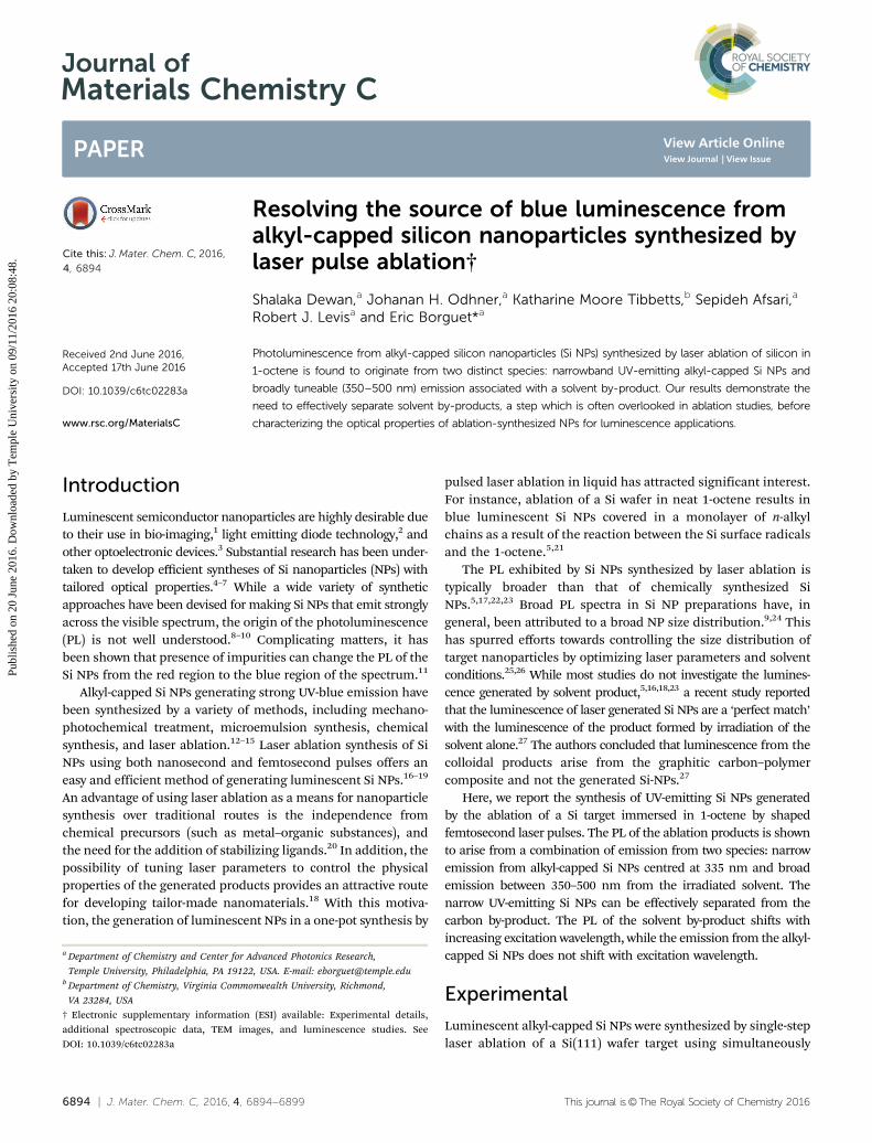
The as-ablated sample shows strong blue PL under a handheld UVlamp (B340 nm) (Fig. 1a inset). The corresponding PL spectracover the range of 300–500 nm (Fig. 1a). The emission red-shifts asthe excitation wavelength is tuned from 260 to 400 nm (Fig. 1a),consistent with previous reports on Si NPs generated by laserablation.5,17,22 The PL spectra have peak widths of B100 nm(FWHM) over the whole range. The peak emission intensity isobserved at B330 nm (3.75 eV) with 280 nm (4.43 eV) excitation,in agreement with results obtained for chemically synthesizedheptyl-capped Si NPs.31 However, this PL is broader than that ofchemically synthesized alkyl-capped Si NPs,31–33 an observationthat has been attributed to a broad particle size distribution.8
While most ablation studies do not discuss the influence of thelaser irradiation of the solvent on the PL spectrum,17,23 Intartagliaet al. reported that the PL of Si NPs produced by laser ablation wasidentical to the PL of the irradiated solvent alone.27 The carbonby-product was observed as large, amorphous structures in
Fig. 1 PL from Si NPs generated by shaped femtosecond laser pulseablation of Si in 1-octene. PL spectra (solid lines) and excitation scans(dotted lines) of (a) as-ablated sample before separation and (b) controlsample (irradiation of neat 1-octene). (c) Si NPs after separation of carbonby-product. Inset: As-ablated sample under UV lamp illumination. Stars onthe graphs indicate scattered 2nd order diffraction of the excitationphotons.
Paper Journal of Materials Chemistry C
Publ
ishe
d on
20
June
201
6. D
ownl
oade
d by
Tem
ple
Uni
vers
ity o
n 09
/11/
2016
20:
08:4
8.
View Article Online
6896 | J. Mater. Chem. C, 2016, 4, 6894--6899 This journal is©The Royal Society of Chemistry 2016
TEM images.27 The authors concluded that this carbon by-product,arising from the interaction of the pulsed laser with the solvent,accounted for the majority of the emission generated by the productsof pulsed laser ablation of Si in toluene under the conditionsreported.27 Similar amorphous carbon structures were observed inour TEM images of the as-ablated products (Fig. S3, ESI†).
To determine the influence of the solvent on the observed PL ofthe as-ablated sample, 1-octene was irradiated under the sameconditions as above but without the Si target. The products ofsolvent irradiation luminesced between 350–500 nm, and thespectrum was observed to red-shift as the excitation wavelength(Fig. 1b) was tuned to wavelengths 4300 nm. However, contrary tothe previous study by Intartaglia et al., the PL of this control wasdifferent from that of the as-ablated sample, showing no intensityo350 nm. In our as-ablated samples, the difference between Si NPPL and that of solvent irradiation control is quite obvious (Fig. 1aand b), possibly because of the differences in the laser source usedhere (for e.g., different wavelength and pulse width).
The similar emission profiles (Fig. 1a and b) at excitationwavelengths above 300 nm suggest that the luminescent productof 1-octene irradiation may also be generated in the ablationsynthesis of Si NPs in the presence of 1-octene. The PL of theirradiated solvent is similar to that observed from carbon andgraphene quantum dots, as well as from toluene irradiation.34–36
Moreover, the excitation spectra of the as-ablated samplerecorded for emission at 340 nm are blue-shifted with respectto the control (peaking at 290 nm as opposed to 310 nm, Fig. 1aand b). These findings suggest that the Si NPs generated by laserablation have optical properties that are different from those ofthe carbon by-product and it may be possible to resolve them.
With this objective in mind, the separation of the carbonand silicon irradiation products was performed by centrifugationThe PL spectrum of the alkyl-capped Si NPs after separation ofthe carbon by-product (Fig. 1c) is significantly different from theas-ablated Si NPs (Fig. 1a); moreover, the fluorescence is also
narrower than that previously reported for laser ablated, alkyl-capped Si NPs.17,23,37,38 The PL of the separated Si NPs, centred at335 nm (3.64 eV), is consistent with that of chemically synthesizedalkyl-capped Si NPs,8,31,33 where emission in the B330–360 nmregion was attributed to be a result of electron–hole recombinationacross the direct G point transition in silicon (3.4 eV).10,39 The blue-shift to 3.64 eV from 3.4 eV was said to be a result of quantumconfinement.39 The emission spectrum does not red-shift withincreasing excitation wavelength, but only changes in amplitude,indicating that the PL likely originates from a direct band gaptransition.5 Low intensity PL observed in the separated Si NPsbetween 350 nm and 500 nm, for excitation at wavelengths4350 nm, is attributed to residual carbon by-product not removedin the centrifugation step. Since only one size distribution wassynthesized in the experiments reported here, it was not possible tomeasure the effect of particle size on the PL spectrum and nodefinitive conclusions about the role of quantum confinement canbe made. We note that the PL spectrum of the separated Si NPs wasthe same for all laser energies used during ablation (Fig. S4, ESI†).
The PL spectra of the separated carbon by-product (Fig. S5,ESI†) are very similar to those of the irradiated 1-octene control,suggesting that the origin of the broad, tuneable emission in theas-ablated sample is a result of a carbon by-product generated inthe solvent and is unrelated to the size of the Si nanoparticles.The contribution of the laser ablation by-product to the PL of SiNPs is an important consideration in the application of pulsed-laser ablation as the synthetic route for optical nanostructures.These observations highlight the need to separate the targetmaterial from undesirable by-products.
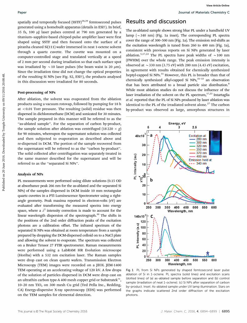
The successful separation of the carbon by-product from theSi NPs was verified by individually analysing the isolated productsby EDS on selected TEM images. EDS mapping revealed a highconcentration of silicon (Fig. 2a(ii)), coincident with the particles(Fig. 2a(i)), in the separated Si NP sample. The uniform distributionof carbon (Fig. 2a(iv)) in the separated Si NP sample originates from
Fig. 2 EDS maps of TEM image of separated Si NPs: TEM images (i) of (a) separated Si NPs and (b) separated carbon by-product, along with thecorresponding EDS map showing intensity for (ii) Si K alpha line, (iii) oxygen K alpha line, and (iv) carbon K alpha line.
Journal of Materials Chemistry C Paper
Publ
ishe
d on
20
June
201
6. D
ownl
oade
d by
Tem
ple
Uni
vers
ity o
n 09
/11/
2016
20:
08:4
8.
View Article Online
This journal is©The Royal Society of Chemistry 2016 J. Mater. Chem. C, 2016, 4, 6894--6899 | 6897
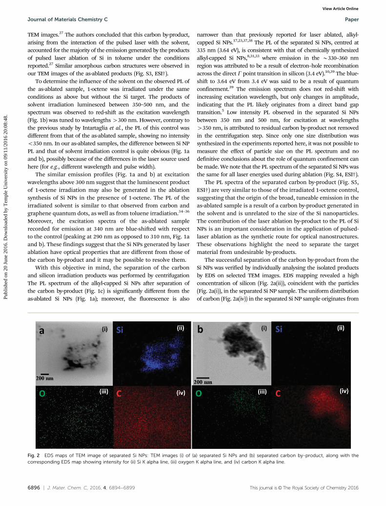
the grid itself and confirms the effective separation of Si NPs fromthe solvent derived carbon product. On the other hand, no silicon Kalpha emission is observed in the carbon by-product (Fig. 2b(ii)),but there are clearly carbon particles on the grid that can bedistinguished from the background from the carbon grid itself(Fig. 2b(iv)). Low concentrations of oxygen are detected on bothgrids (Fig. 2a and b(iii)). Representative TEM images (Fig. 3) of theseparated Si NPs show areas containing very small (o2 nm)particles (Fig. 3a) as well as areas containing larger B5–10 nmparticles (Fig. 3b and c), with an average diameter of 3.4 nm(Fig. 3d) for a sample of 260 objects.
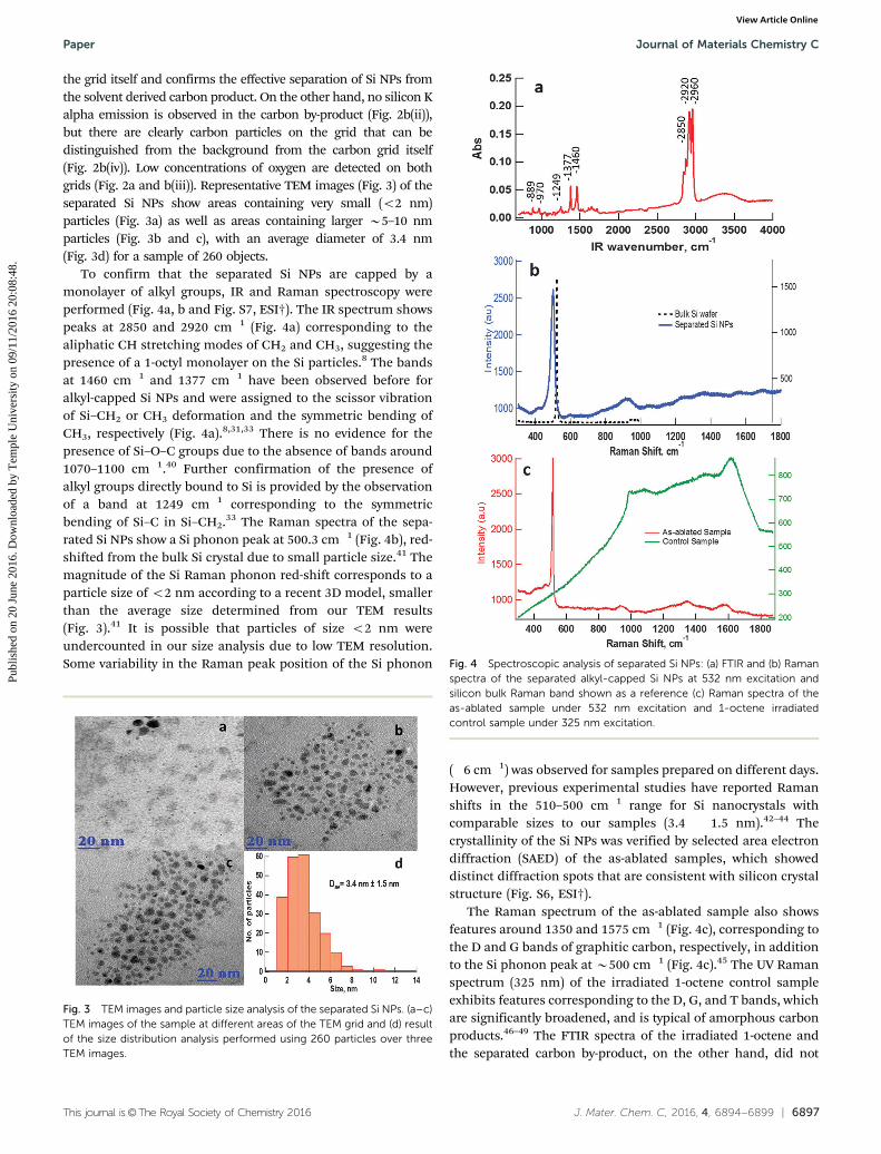
To confirm that the separated Si NPs are capped by amonolayer of alkyl groups, IR and Raman spectroscopy wereperformed (Fig. 4a, b and Fig. S7, ESI†). The IR spectrum showspeaks at 2850 and 2920 cm�1 (Fig. 4a) corresponding to thealiphatic CH stretching modes of CH2 and CH3, suggesting thepresence of a 1-octyl monolayer on the Si particles.8 The bandsat 1460 cm�1 and 1377 cm�1 have been observed before foralkyl-capped Si NPs and were assigned to the scissor vibrationof Si–CH2 or CH3 deformation and the symmetric bending ofCH3, respectively (Fig. 4a).8,31,33 There is no evidence for thepresence of Si–O–C groups due to the absence of bands around1070–1100 cm�1.40 Further confirmation of the presence ofalkyl groups directly bound to Si is provided by the observationof a band at 1249 cm�1 corresponding to the symmetricbending of Si–C in Si–CH2.33 The Raman spectra of the sepa-rated Si NPs show a Si phonon peak at 500.3 cm�1 (Fig. 4b), red-shifted from the bulk Si crystal due to small particle size.41 Themagnitude of the Si Raman phonon red-shift corresponds to aparticle size of o2 nm according to a recent 3D model, smallerthan the average size determined from our TEM results(Fig. 3).41 It is possible that particles of size o2 nm wereundercounted in our size analysis due to low TEM resolution.Some variability in the Raman peak position of the Si phonon
(�6 cm�1) was observed for samples prepared on different days.However, previous experimental studies have reported Ramanshifts in the 510–500 cm�1 range for Si nanocrystals withcomparable sizes to our samples (3.4 � 1.5 nm).42–44 Thecrystallinity of the Si NPs was verified by selected area electrondiffraction (SAED) of the as-ablated samples, which showeddistinct diffraction spots that are consistent with silicon crystalstructure (Fig. S6, ESI†).
The Raman spectrum of the as-ablated sample also showsfeatures around 1350 and 1575 cm�1 (Fig. 4c), corresponding tothe D and G bands of graphitic carbon, respectively, in additionto the Si phonon peak at B500 cm�1 (Fig. 4c).45 The UV Ramanspectrum (325 nm) of the irradiated 1-octene control sampleexhibits features corresponding to the D, G, and T bands, whichare significantly broadened, and is typical of amorphous carbonproducts.46–49 The FTIR spectra of the irradiated 1-octene andthe separated carbon by-product, on the other hand, did not
Fig. 3 TEM images and particle size analysis of the separated Si NPs. (a–c)TEM images of the sample at different areas of the TEM grid and (d) resultof the size distribution analysis performed using 260 particles over threeTEM images.
Fig. 4 Spectroscopic analysis of separated Si NPs: (a) FTIR and (b) Ramanspectra of the separated alkyl-capped Si NPs at 532 nm excitation andsilicon bulk Raman band shown as a reference (c) Raman spectra of theas-ablated sample under 532 nm excitation and 1-octene irradiatedcontrol sample under 325 nm excitation.
Paper Journal of Materials Chemistry C
Publ
ishe
d on
20
June
201
6. D
ownl
oade
d by
Tem
ple
Uni
vers
ity o
n 09
/11/
2016
20:
08:4
8.
View Article Online
6898 | J. Mater. Chem. C, 2016, 4, 6894--6899 This journal is©The Royal Society of Chemistry 2016
show any aromatic or aliphatic C–H stretch features, (Fig. S7a,ESI†), suggesting that the carbon by-product may also containamorphous carbon. The determination of the exact compositionof the carbon by-product will be the efforts of future studies.
Conclusions
We have demonstrated that the broad, tuneable photoluminescencereported for silicon nanoparticles synthesized by laser ablation inorganic liquids originates from two different species that can beseparated as: narrow-band, UV-emitting alkyl-capped Si NPs and asolvent irradiation carbon by-product whose emission is relativelybroad and tuneable from 350–500 nm. Contrary to the findings ofprevious studies,27,45 our results show that the PL of Si NPs is notonly different from that generated by laser interaction with thesolvent, but, once separated, the emission from alkyl-capped Si NPs,centred at 335 nm (3.64 eV), looks remarkably similar to the PL ofchemically synthesized alkyl-capped Si NPs.31 Our results show thatluminescent carbon by-products formed during laser ablation in anorganic solvent can be systematically removed from the Si NPs,revealing the UV emission of alkyl-capped SI NPs. This studyhighlights importance of separating reaction by-products beforeconsidering the optical properties of nanostructures producedby laser ablation in solvent.
Acknowledgements
Support of this research by the Army Research Laboratory throughcontract W911NF-10-2-009 is gratefully acknowledged. The authorsacknowledge NSF instrumentation grant (CHE-0923077) for theJEOL JEM-1400 TEM used in this research. Authors thank theSieburth Lab for assistance in sample processing. TEM grids weregenerously provided by Neretina Lab. SD thanks Gregory Fiorin forassistance with Raman experiments.
Notes and references
1 F. Erogbogbo, K. T. Yong, I. Roy, G. Xu, P. N. Prasad andM. T. Swihart, ACS Nano, 2008, 2, 873–878.
2 F. Maier-Flaig, J. Rinck, M. Stephan, T. Bocksrocker, M. Bruns,C. Kubel, A. K. Powell, G. A. Ozin and U. Lemmer, Nano Lett.,2013, 13, 475–480.
3 V. Biju, T. Itoh, A. Anas, A. Sujith and M. Ishikawa, Anal.Bioanal. Chem., 2008, 391, 2469–2495.
4 T. M. Atkins, A. Y. Louie and S. M. Kauzlarich, Nanotechnology,2012, 23, 294006.
5 N. Shirahata, M. R. Linford, S. Furumi, L. Pei, Y. Sakka,R. J. Gates and M. C. Asplund, Chem. Commun., 2009,4684–4686.
6 N. Arul Dhas, C. P. Raj and A. Gedanken, Chem. Mater.,1998, 10, 3278–3281.
7 L. Mangolini, E. Thimsen and U. Kortshagen, Nano Lett.,2005, 5, 655–659.
8 N. Shirahata, T. Hasegawa, Y. Sakka and T. Tsuruoka, Small,2010, 6, 915–921.
9 J. P. Wilcoxon and G. A. Samara, Appl. Phys. Lett., 1999, 74,3164–3166.
10 S. Yang, W. Li, B. Cao, H. Zeng and W. Cai, J. Phys. Chem. C,2011, 115, 21056–21062.
11 M. Dasog, Z. Yang, S. Regli, T. M. Atkins, A. Faramus, M. P.Singh, E. Muthuswamy, S. M. Kauzlarich, R. D. Tilley andJ. G. C. Veinot, ACS Nano, 2013, 7, 2676–2685.
12 D. S. English, L. E. Pell, Z. Yu, P. F. Barbara and B. A. Korgel,Nano Lett., 2002, 2, 681–685.
13 K. Kusova, O. Cibulka, K. Dohnalova, I. Pelant, J. Valenta,A. Fucıkova, K. Zıdek, J. Lang, J. Englich, P. Matejka,P. Stepanek and S. Bakardjieva, ACS Nano, 2010, 4,4495–4504.
14 N. Shirahata, D. Hirakawa and Y. Sakka, Green Chem., 2010,12, 2139–2141.
15 J. R. Siekierzycka, M. Rosso-Vasic, H. Zuilhof and A. M.Brouwer, J. Phys. Chem. C, 2011, 115, 20888–20895.
16 H. Zeng, X.-W. Du, S. C. Singh, S. A. Kulinich, S. Yang, J. Heand W. Cai, Adv. Funct. Mater., 2012, 22, 1333–1353.
17 D. Tan, Z. Ma, B. Xu, Y. Dai, G. Ma, M. He, Z. Jin and J. Qiu,Phys. Chem. Chem. Phys., 2011, 13, 20255–20261.
18 S. Hamad, G. K. Podagatlapalli, V. S. Vendamani, S. V. S.Nageswara Rao, A. P. Pathak, S. P. Tewari and S. VenugopalRao, J. Phys. Chem. C, 2014, 118, 7139–7151.
19 S. Alkis, A. K. Okyay and B. Ortaç, J. Phys. Chem. C, 2012,116, 3432–3436.
20 S. Barcikowski and G. Compagnini, Phys. Chem. Chem. Phys.,2013, 15, 3022–3026.
21 V. Amendola and M. Meneghetti, Phys. Chem. Chem. Phys.,2013, 15, 3027–3046.
22 L. Wanbing, W. Liping, Y. Wei, W. Xinzhan, L. Xiaowei andF. Guangsheng, Micro Nano Lett., 2012, 7, 1125–1128.
23 K. Abderrafi, R. l. Garcıa Calzada, M. B. Gongalsky, I. Suarez,R. Abarques, V. S. Chirvony, V. Y. Timoshenko, R. Ibanez andJ. P. Martınez-Pastor, J. Phys. Chem. C, 2011, 115, 5147–5151.
24 N. Shirahata, Phys. Chem. Chem. Phys., 2011, 13, 7284–7294.25 L. Patrone, D. Nelson, V. Safarov, M. Sentis and W. Marine,
J. Lumin., 1998, 80, 217–221.26 P. G. Kuzmin, G. A. Shafeev, V. V. Bukin, S. V. Garnov,
C. Farcau, R. Carles, B. Warot-Fontrose, V. Guieu andG. Viau, J. Phys. Chem. C, 2010, 114, 15266–15273.
27 R. Intartaglia, K. Bagga, A. Genovese, A. Athanassiou,R. Cingolani, A. Diaspro and F. Brandi, Phys. Chem. Chem.Phys., 2012, 14, 15406–15411.
28 J. H. Odhner, K. M. Tibbetts, B. Tangeysh, B. B. Waylandand R. J. Levis, J. Phys. Chem. C, 2014, 118, 23986–23995.
29 B. Tangeysh, K. Moore Tibbetts, J. H. Odhner, B. B. Waylandand R. J. Levis, J. Phys. Chem. C, 2013, 117, 18719–18727.
30 J. Mooney and P. Kambhampati, J. Phys. Chem. Lett., 2013, 4,3316–3318.
31 R. D. Tilley, J. H. Warner, K. Yamamoto, I. Matsui andH. Fujimori, Chem. Commun., 2005, 1833–1835.
32 F. Hua, M. T. Swihart and E. Ruckenstein, Langmuir, 2005,21, 6054–6062.
33 C.-S. Yang, R. A. Bley, S. M. Kauzlarich, H. W. H. Lee andG. R. Delgado, J. Am. Chem. Soc., 1999, 121, 5191–5195.
Journal of Materials Chemistry C Paper
Publ
ishe
d on
20
June
201
6. D
ownl
oade
d by
Tem
ple
Uni
vers
ity o
n 09
/11/
2016
20:
08:4
8.
View Article Online
This journal is©The Royal Society of Chemistry 2016 J. Mater. Chem. C, 2016, 4, 6894--6899 | 6899
34 S. Yang, H. Zeng, H. Zhao, H. Zhang and W. Cai, J. Mater.Chem., 2011, 21, 4432–4436.
35 Y. Dong, J. Shao, C. Chen, H. Li, R. Wang, Y. Chi, X. Lin andG. Chen, Carbon, 2012, 50, 4738–4743.
36 H. Li, X. He, Z. Kang, H. Huang, Y. Liu, J. Liu, S. Lian,C. H. A. Tsang, X. Yang and S.-T. Lee, Angew. Chem., Int. Ed.,2010, 49, 4430–4434.
37 N. Mansour, A. Momeni, R. Karimzadeh and M. Amini, Opt.Mater. Express, 2012, 2, 740–748.
38 J. Wang, S. Sun, F. Peng, L. Cao and L. Sun, Chem. Commun.,2011, 47, 4941–4943.
39 J. P. Wilcoxon, G. A. Samara and P. N. Provencio, Phys. Rev.B: Condens. Matter Mater. Phys., 1999, 60, 2704–2714.
40 K. A. Pettigrew, Q. Liu, P. P. Power and S. M. Kauzlarich,Chem. Mater., 2003, 15, 4005–4011.
41 G. Faraci, S. Gibilisco, A. R. Pennisi and C. Faraci, J. Appl.Phys., 2011, 109, 074311.
42 C. M. Hessel, J. Wei, D. Reid, H. Fujii, M. C. Downer andB. A. Korgel, J. Phys. Chem. Lett., 2012, 3, 1089–1093.
43 C. Meier, S. Luttjohann, V. G. Kravets, H. Nienhaus, A. Lorkeand H. Wiggers, Phys. E, 2006, 32, 155–158.
44 H. Xia, Y. L. He, L. C. Wang, W. Zhang, X. N. Liu, X. K. Zhang,D. Feng and H. E. Jackson, J. Appl. Phys., 1995, 78, 6705–6708.
45 S. Hamad, G. Krishna Podagatlapalli, R. Mounika, S. V. S.Nageswara Rao, A. P. Pathak and S. Venugopal Rao, AIP Adv.,2015, 5, 127127.
46 A. C. Ferrari and J. Robertson, Phys. Rev. B: Condens. MatterMater. Phys., 2001, 64, 075414.
47 S. Osswald, G. Yushin, V. Mochalin, S. O. Kucheyev andY. Gogotsi, J. Am. Chem. Soc., 2006, 128, 11635–11642.
48 K. W. Gilkes, H. S. Sands, D. N. Batchelder, J. Robertson andW. I. Milne, Appl. Phys. Lett., 1997, 70(15), 1980–1982.
49 V. I. Merkulov, J. S. Lannin, C. H. Munro, S. A. Asher, V. S.Veerasamy and W. I. Milne, Phys. Rev. Lett., 1997, 78, 4869–4872.
Paper Journal of Materials Chemistry C
Publ
ishe
d on
20
June
201
6. D
ownl
oade
d by
Tem
ple
Uni
vers
ity o
n 09
/11/
2016
20:
08:4
8.
View Article Online