Embed Size (px)
Citation preview

JOURNAL OF LATEX CLASS FILES, VOL. 14, NO. 8, AUGUST 2015 1
Approximate MRAM: High-performance andPower-efficient Computing with MRAM Chips for
Error-tolerant ApplicationsFarah Ferdaus, Student Member, IEEE, B. M. S. Bahar Talukder, Student Member, IEEE, and Md Tauhidur
Rahman, Member, IEEE
Abstract—Approximate computing (AC) leverages the inherent error resilience and is used in many big-data applications from variousdomains such as multimedia, computer vision, signal processing, and machine learning to improve systems performance and powerconsumption. Like many other approximate circuits and algorithms, the memory subsystem can also be used to enhance performanceand save power significantly. This paper proposes an efficient and effective systematic methodology to construct an approximatenon-volatile magneto-resistive RAM (MRAM) framework using consumer-off-the-shelf (COTS) MRAM chips. In the proposed scheme,an extensive experimental characterization of memory errors is performed by manipulating the write latency of MRAM chips whichexploits the inherent (intrinsic/extrinsic process variation) stochastic switching behavior of magnetic tunnel junctions (MTJs). Theexperimental results and error-resilient image application reveal that the proposed AC framework provides a significant performanceimprovement and demonstrates a maximum reduction in MRAM write current of ∼66% on average with negligible or no loss in outputquality.
Index Terms—Approximate Computing, MRAM, Cache Write Policy, Low Power Design, Approximate MRAM.
F
1 INTRODUCTION
THE amount of unstructured data processing from nu-merous modern computing platforms from mobile to
the cloud is increasing rapidly, requiring an efficient frame-work to mitigate the gap between processor and memorysystem and accomplish the computational and storage de-mands of the current computing system even in advancedmulti-core processors. Besides, nowadays, memories con-sume a significant power and chip area, becoming thecomputing system’s main bottleneck. Moreover, continualscaling down in technology introduces immense challengessuch as notable power consumption, substantial processvariation, crucial transistor’s sensitivity with different op-erating conditions, etc., to the conventional memory chips.Existing mainstream volatile memory chips, i.e., static RAM(SRAM) and dynamic RAM (DRAM), suffer from density,scalability, memory persistency, and leakage issues. Besides,current non-volatile memory (NVM) chips (e.g., Flash) suf-fer from endurance and performance problems. These lim-itations make existing memory chips incompetent for de-livering ever-increasing demands of power-efficient, high-performance systems with the growing number of cores anddataset sizes [1].
Fortunately, data-intensive emerging applications incomputer vision, graphics, multimedia, recognition, datamining, data-driven inference, and machine learning exhibitintrinsic error resilience property provide scopes of produc-ing acceptable quality outputs even with data or computa-tion approximations [2]. By leveraging such applications’ in-trinsic error tolerance nature, approximate computing (AC)
The authors are with the Department of Electrical and Computer Engineering,Florida International University, Miami, FL, 33174.E-mail: fferd006, bbaha007, [email protected] received April 19, 2005; revised August 26, 2015.
attains performance and power improvement by orders ofmagnitude using software, architecture, and circuit-leveltechniques [2], [3]. Therefore, these intrinsic characteristicsof applications endow producing good-enough quality re-sults even in noisy or slightly erroneous imprecise inputs.Hence, attracting great interest in designing or implement-ing approximate memories by relaxing the strict constraintsin a controlled manner on data integrity, in turn, savessignificant power consumption as well as improves perfor-mance notably.
MRAM chip has significant potential to turn into a domi-nant universal memory (cache or main memory) technologydue to its promising scopes such as non-volatility, scalability,high speed and fast access latencies, unlimited endurance,ultralow-power operation, CMOS compatibility, high den-sity, reliability, near-zero leakage, almost zero static power,thermal robustness, and radiation hardness [4]. These ad-vantageous features make MRAM suitable to integrate intomost of the systems. Therefore, MRAM can be an attractivecandidate for energy efficiency on-chip memory. However,the higher write current for a sufficiently long duration isrequired for proper magnetic switching during the writeoperation still limits their overall energy efficiency. Severalpromising research has been performed on the circuit, de-vice, and architecture levels to improve the energy efficiencyof MRAM [5], [6], [7], [8]. This paper proposes a newdimension of MRAM-based approximate approach to attainsignificant power savings by introducing a small number oferrors that most error-resilient applications can endure.
The major challenge in AC is managing the approxima-tions to achieve the most favorable application quality vs.energy trade-off. Most AC-based prior works are focusedon processing or logic circuits and can be categorized based
arX
iv:2
105.
1415
1v1
[cs
.ET
] 2
9 M
ay 2
021
JOURNAL OF LATEX CLASS FILES, VOL. 14, NO. 8, AUGUST 2015 2
on the targeted memory hierarchy level [9], [10], [11], [12],[13], [14]. These works focus on (i) secondary storage andmain memory [9], [10], (ii) application-specific memorydesigns [11], [12], and (iii) CMOS memory-based approx-imate cache architecture [13], [14]. However, the existingMRAM-based AC framework is mostly simulation-based,requires extension in either new instruction set architecture(ISA) or enhancement in cache replacement policies alongwith device-circuit-architecture remodeling [8], [12]. Hence,these MRAM-based AC frameworks can not be easily in-tegrated into the existing computing system due to theabove-mentioned strict requirements. The previous contri-butions inspirit the need for real memory implementationand build the foundation of the proposed MRAM-based ACframework using consumer-off-the-shelf (COTS) MRAMchips, which require minimal or no additional hardware,is robust against environmental fluctuations. Towards thisend, our proposed system-level MRAM-based experimentalAC framework yields significant power benefits for smallprobabilities of write failures by exploiting write latencyvariations of COTS MRAM chips.
This paper presents a new approach to constructingan approximate MRAM framework. We also introduce adata allocation scheme based on the cell characterizationalgorithm for the proposed framework. The core idea isthat at sub-optimal write latency, MRAM addresses canbe split into accurate and approximate addresses throughextensive error characterization of COTS toggle MRAMchips. The correlation between the obtained errors and theapplication-level output quality guides the proper allocationof application data to MRAM addresses. The more straight-forward implementation of the proposed mechanism resultsin a better power-quality trade-off. In summary, the keycontributions of this work are as follows.• We reduce the write enable (W ) time from the man-
ufacturer’s recommended value during the write op-eration to introduce errors. We perform an extensivecharacterization of these errors using COTS Everspintoggle MRAM chips [15] to improve write power ef-ficiency by exploiting the applications’ error-resilientnature. The characterization results are used to de-rive key insights about memory errors — for exam-ple, toggling from ’1‘→ ’0‘ and ’0‘→ ’1‘ are mutuallyexclusive.
• Insights obtained from the characterization guide usin constructing a systematic data allocation schemebased on the application requirements to store criticaland approximate data considering the occurrenceand properties of MRAM errors by writing differ-ent intuitive and non-intuitive input data patterns.Subsequently, approximate data can be stored in theapproximate addresses, whereas critical data must beallocated in entirely accurate memory addresses.
• We analyze a detailed trade-off between theapplication-level output accuracy and system-levelperformance/power gains by determining optimalwrite latency.
• We implement our AC framework using our custommemory controller implemented on Xilinx Artix 7(XC7A35T-1C) FPGA to manipulate different timinglatency of a couple of emerging memories [16]. Our
experimental results demonstrate a significant im-provement in the power-quality trade-off and showan average maximum write current savings of ∼66%with minimal or no loss in application quality.
The rest of the paper is organized as follows. Sect.2 provides an overview of related prior work. Sect. 3briefly overviews the organization and operating principleof MRAM chips and related preliminaries of cache writingpolicies. Sect. 4 presents the proposed AC framework, in-cluding the cell characterization algorithm. Sect. 5 explainsthe experimental setup and exhibits obtained results. Sect.6 discusses the characterization and memory overhead re-quired to store the erroneous memory addresses and criticaldata protection. Finally, Sect. 7 concludes the article.
2 RELATED WORK
This work correlates two distinct research areas – emergingMRAM memories with approximate computing. Previoussimulation-based MRAM-related work focuses on address-ing spintronic memories’ high write energy while pre-serving accurate read/write operations to achieve energy-efficient on-chip memories using the circuit, architectural,and device-level techniques [6], [17], [18], [19], [20], [21],[22]. In [17], using the bit-line voltage clamping technique,MRAM write-current asymmetry is mitigated at the cir-cuit level to achieve the goal. Besides, in [18], a co-designmethodology focusing on the bit-cell access transistor andthe supply voltage is proposed to improve energy efficiency.Moreover, the MRAM cell’s actual switching time detectiontechnique is proposed to cease the unnecessary current flowimmediately after a complete write [21], [23]. Significantwrite energy reduction is achieved for such techniques;however, the overall write latency remains the same. Onthe other hand, at the architectural level, in [19], [20], theproposed hybrid CMOS-spintronic cache can selectively di-rect the write-intensive memory blocks to the CMOS portionwhile keeping the remaining blocks in the spintronic part toaddress the write-inefficiency of the spintronic memories.Besides, redundant memory writes are eliminated by com-paring the previously stored data before the write operation[21] or tracking dirty data at a finer granularity [22]. In addi-tion, in [24], significant write margin reduction is achievedby exploiting incomplete write operations, and the incom-plete bits are processed through robust Error CorrectionCodes (ECCs) at the cost of large decoding latencies (impair-ing the memory read latency). Furthermore, at the devicelevel, in [6], [25], volatile spintronic memory is proposedby relaxing the non-volatility property (data-retention-time)or the current to overcome high write latency and energyissues of STT-MRAMs alongside the proposed refresh tech-niques can avoid data retention errors at the cost of highererror rate. Besides, in [26], the thermal stability factor [27],which defines the stability of the free layer’s magnetic orien-tation against thermal noise, is reduced to address extremewrite margin at the cost of higher overall failure rate andretention time.
On the other hand, the previous AC-based frameworkexplores different layers of abstraction spanning softwareor circuits, architectures, and algorithms to reduce the con-sumed energy in processing cores/accelerators. Introducingerrors in the memory subsystem is an effective way of
JOURNAL OF LATEX CLASS FILES, VOL. 14, NO. 8, AUGUST 2015 3
exploiting the applications’ intrinsic error resilience. How-ever, we concentrate on prior works related to approx-imate memories since that aligns with this work. Priorworks on approximate DRAMs [9], [10] relax their refreshrate to inject retention errors in the saved or read datacontents in exchange for refresh power savings. On theother hand, [28] proposes approximate multilevel PCMsthat can (i) reduce the number of programming pulsesto inject write errors in exchange for energy savings and(ii) perform partial error correction on the most significantbits of the worn-out blocks. However, spintronic memoriesrequire exploring new techniques due to the in-applicabilityof the mentioned approximation mechanisms. Moreover,[12] proposes simulation-based enhanced architectural andsoftware approximate design models by accessing cells inthe memory arrays with different current levels dependingon application requirements at the cost of higher read/writeerror rates, that can (i) specify acceptable error probabil-ities for groups of bits within the word by controllingthe quality of the read/write operations (ii) regulate (bysoftware) the numerical significance of errors incurred dur-ing approximate load/store operations. However, this workentirely ignores the process variation effect. The processvariation in spintronic memories affects both the MTJ celland CMOS transistor parameters, which, in turn, impactsthe parameters associated with read/write operations suchas switching current, thermal stability factor, transistor’soutput current, etc. Consequently, the output accuracy atthe architecture level will vary considerably with processvariation due to these different and lower read/write ac-cess current levels. Furthermore, in [8], another simulation-based new approximate spintronic on-chip memory designis proposed by relaxing both device and circuit parametersof spintronic memories by increasing various failure ratessuch as read disturb, retention and read decision failures,along with write errors to improve energy consumption andperformance.
In contrast, our work renders an power-quality trade-off through a real memory implementation by employingCOTS MRAM chips that (i) require minimal or no additionalhardware, (ii) are robust against environmental fluctuations,and (iii) achieve power and performance improvementsover and beyond the previous techniques, which is the keyuniqueness of the proposed work.
3 BACKGROUND
3.1 MRAM: PreliminariesThe core element of toggle MRAM is the Magnetic tunneljunction (MTJ) that uses the Savtchenko switching [29] prop-erty by creating a rotating field with the sequential identicalwrite current pulses to store both data states (high and low).The 1T-1MTJ MRAM bit cell comprises two ferromagneticlayers separated by a thin dielectric tunnel oxide (AlOx orMgO) layer, built using advanced thin-film processing tech-nology (shown in Fig. 1a). One layer’s magnetic orientationis permanently fixed, commonly referred to as the refer-ence (or fixed) magnetic layer (RML). In contrast, the otherlayer’s magnetization can freely be oriented depending onthe magnetic field and known as the free magnetic layer(FML). The FML is composed of NiFe synthetic antiferro-magnet (SAF). The substantially higher magnetic anisotropy
of RML compared to FML ascertains stable magnetizationdirection of FML during memory read/write operation. Theresistance states determine the bit which is going to store inthe memory array. When both the FML and RML are alignedin the same direction (a large current passed from SelectLine(SL) to BitLine (BL) through the barrier layer), the MTJproduces low electrical resistance. On the other hand, whentheir magnetic field orientation is opposite, the resistancebecomes extremely large; hence, almost no current or only aweak current flows through the barrier layer. Therefore, theMTJ exhibits high electrical resistance.
Writing a bit in the magnetic field-driven toggle MRAMarray requires passing a high write current (Iw) for changingFML’s magnetic orientation [29]. The applied Iw to the writelines, placed on top and bottom of the MTJ devices (see Fig.1a), creates an auxiliary magnetic field that changes the FMLdirection in the required position. Contrastingly, the RML’sdirection is strongly coupled with an anti-ferromagnet [29].During the write operation, the memory circuit performsa pre-read operation to determine the state of the targetbit and execute a toggle pulse (if required) to change thestate of the bit if the desired state is not the same as thetargeted state. Consequently, it reduces the overall powerconsumption and improves power efficiency. However, thisincreases the total write cycle time (including an additionalread operation).
A small bias voltage (far below the device’s breakdownvoltage) is applied across the MRAM cell during the readcycle. Depending on parallel (RLow) or anti-parallel (RHigh)magnetic orientation, a current sensing circuitry that isattached with the MRAM cell experiences different currentand latches the appropriate logic (‘0’ or ‘1’) comparingwith the reference resistance (RRef ) shown in Fig. 1b. Therandom resistance variation effect of a larger-sized MRAMarray read circuitry is illustrated in Fig. 1b. The accepted bitsare those whose statistical separation is greater than 5σ fromthe mean, where σ is the standard deviation. The accuracyof the read circuitry entirely depends on determining theactual resistance state in the tail region (useable resistancechange, ∆RUse) of the distribution. For robust operation,less noise-sensitive, and high-speed read operation withnormal process variation, large ∆RUse, and significantlymore than 12σ separation are crucial [29]. Furthermore,the width of resistance distribution varies from cell tocell because of manufacturing process variations. Besides,the quality, size, and level of in-homogeneity of the MTJtunnel barrier significantly impact larger relative bit-to-bitresistance variation [29]. Therefore, a thicker tunnel barrier(∼ 1nm) is essential to maintain the resistance level of theMTJ in the kilo Ω range for minimizing the series resistanceeffect from the isolation transistor [29], where Ω is the SIunit of resistance.
Magnetic state-based data storage has several advan-tages over charge-based storage, i.e., non-destructive readoperation, no leakage during magnetic polarization, un-limited read/write endurance, no wear-out due to nomovement of electrons/atoms during the switching pro-cess of magnetic polarization, etc. [31]. Besides, Savtchenkoswitching-based MRAM arrays possess several importantperformance characteristics, such as lower write error rateand fast read/write cycle (35ns). Less sensitivity to external

JOURNAL OF LATEX CLASS FILES, VOL. 14, NO. 8, AUGUST 2015 4
Write Current
Write Current
Magnetic Field
Magnetic Field
AlOx
Parallel (low R)
AlOx
Anti-Parallel (high R)
(a)
Cell Resistance
Pro
bab
ility
RHighRLow
RRef
ΔRUse
ΔR
6σLow 6σHigh
(b)
Magnetic Field
Resistance
(c)Fig. 1: (a) Toggle MRAM cell structure with MTJ. (b) Schematic representation of Gaussian resistance (RLow andRHigh states) distribution of larger-sized MTJ array [29]. (c) Principle of tunneling magnetoresistance (TMR) [30].
fields makes them less sensitive to manufacturing processvariations [32]. However, from Fig. 1c, we observe thatthe change in resistance due to the change in the inducedmagnetic field is steep in a certain region (the green regionon Fig. 1c). In this region, a slight change in the inducedmagnetic field may cause a drastic change in resistancestates and alter the decision of the read circuitry. Therefore,manufacturers define timing parameters for all commercialmemory chips for reliable write/read operation of the mem-ories against a wide range of operating conditions. For tog-gle MRAM, three different control parameters can governthe write operation of the MRAM chip: write enable (W ),chip enable (E), and upper/lower byte enable (UB/LB)signals [15]. A simplified version of the write enable (W )controlled write operation of the MRAM chip is shown inFig. 2.
ADDR WELOW ADDRWEHIGH
tWC
tW
tWR
Data I/O
Command
Valid Data
tDV
Fig. 2: Write enable (W ) controlled write cycle of MRAM.
Here,tWC = write cycle time, i.e., the time period to complete
full write operation in a particular address.tW = write pulse width, i.e., the time period for which the
W pin is kept activated.tWR = write recovery time, i.e., the time to complete the
write operation after the W pin is deactivated.tDV = valid data to end of write, i.e., the time for which the
valid data need to be available in the data I/O before the Wpin is deactivated.
If the output enable (G) becomes active simultaneouslyor after W is activated, the output will remain in the highimpedance state. After all three write control parameters (E,W , or UB/LB) become disabled, the G signal must remainin the steady-state high for at least 2ns. Reducing any ofthese timing parameters can improve the speed and reducepower consumption but may lead to faulty operation. Thewrite timing parameter tW is manipulated in this work tointroduce errors during the W -controlled write operation.
3.2 Read vs. Write LatencyMRAM has the potential to be used both as the mainmemory and the cache. Due to the technology limitation, theMRAM is still much slower than the most commonly used
SRAM cache (∼35ns access time on MRAM vs. ∼2–20nsaccess time on SRAM cache). Hence, in this section, we willkeep our discussion limited by considering MRAM as themain memory. However, it is worth mentioning that ourproposed reducing MRAM write latency strategy will alsoimprove the system performance, even if it is used as acache.
In a computer system, the main memory is only accessedwhen there is a cache miss (read/write miss). Usually,recovering a read miss is a direct procedure; i.e., when aread miss occurs, the corresponding memory block (usuallyconsists of multiple data words) of the main memory iscopied directly to the cache. However, by taking propercaution at the software level, one can maximize the cache hitrate and hide the read access latency of the main memory.For example, in a modern computer processor, the averagecache miss rate is <8% for most use-cases [33]. On the otherhand, handling a write miss is more complex. Usually, mostof the modern processors use either of the following twopolicies- (i) write-through policy with write allocation, (ii)write back policy with no-write allocation [34]. In the firstpolicy, when a write miss occurs, the corresponding data aredirectly modified both on the cache and the main memory.Although this procedure is much simpler, it requires a longtime to proceed; hence, it is not used in high-end processors.On the contrary, the second policy is a three-step procedure-(i) at first, the corresponding memory block is copied fromthe main memory to the cache, (ii) then, the processor onlyupdates the target word in the newly copied cache block,(iii) lastly, when the cache is required to be evicted, thecorresponding memory block is written back to the mainmemory. However, both cache miss policies become morecomplex if some of the memory resources are shared by themultiple processor cores (e.g., L2/L3 caches and the mainmemory) and require a dedicated cache coherency protocol.As the write miss recovery procedure is more complex thanthe read miss, the write miss penalty is much higher than theread miss penalty. Moreover, the write miss penalty mightbecome a critical bottleneck for write-intensive programperformance (e.g., iterative weight updating on neural net-works). Hence, in this work, we aim to reduce such penaltiesby improving the write access time of MRAMs.
Furthermore, big data applications allow data ap-proximation to some extent, motivating us to developan AC framework to investigate the trade-off betweenapplication-level acceptable output accuracy vs. system-level power/performance gain in the memory system.
JOURNAL OF LATEX CLASS FILES, VOL. 14, NO. 8, AUGUST 2015 5
4 APPROXIMATE MRAM FRAMEWORK
Random Savtchenko switching property is exploited at thereduced timing parameter in our proposed methodologyto obtain data approximation at the application level. Atreduced write pulse width, tW , of toggle MRAM (see Fig. 2),all memory cells do not receive sufficient write current andtime to toggle into the intended stable state. These randomvariations are created in the MTJ storage element due to theprocess variation and the non-uniform distribution of thecurrent pulse within the chip, which hinders performingan appropriate write operation in all memory cells. Thatis why the manufacturer specifies a set of timing param-eters for reliable read/write operations. Hence, violation inany of these manufacturer-recommended timing parametersmay cause erroneous/faulty outputs during the read/writeoperation. If the tW is insufficient, there is a high chancethat FML cannot align perfectly with the RML (either sameor opposite direction) and might be settled on an inter-mediate position, resulting in leading the cell resistancebeing halfway between RLow and RHigh [30]. Therefore,at reduced tW , if the resultant cell resistance falls aroundthe ∆RUse region of the resistance distribution (see Fig. 1b)curve, the cell will show indeterministic characteristics andgenerate erroneous bits.
Several steps are involved in our proposed scheme. Atthe reduced tW , MRAM chips create errors, and the totalnumber of errors differs at different reduced tW values. Atfirst, we select the most suitable reduced tW value. Thisselected tW aims to generate erroneous bits at a tolerablerange for the error-resilient applications. Second, we pro-pose a cell selection algorithm to characterize all MRAMcells from a set of measurements by writing a specific datapattern that produces maximum error compared with otherdata patterns to identify the erroneous (approximate) anderror-free (accurate) memory cells/addresses for the ACframework. These two steps must be performed only once tochoose the appropriate number of MRAM cells/addresses.Finally, we collect data by writing all necessary data patternsinto the entire memory to gain valuable insights about thebit errors’ frequency, significance, and nature.
4.1 Appropriate Reduced Time Selection
Appropriate reduced time selection is essential for obtainingthe most favorable trade-off between application qualityand power savings. Towards this end, the experimentalresults reveal that some of the memory cells provide er-roneous outputs if the data is written at the reduced tim-ing parameters [35]. The number of these error-prone cellsvaries within the write pulse activation time range t = [0,tW ]. The total number of erroneous bit cells is counted bychanging the tW and writing different input data patterns atdifferent tW . The main objective is to determine a suitabletW for which the acceptable amount of erroneous bits isachieved. The number of erroneous cells is calculated fromall achievable reduced write timing parameters in the nextstep. Finally, we propose an algorithm to characterize theerroneous memory cells for the AC framework using thetiming parameter for which the sustainable amount of errorbits is obtained.
4.2 Erroneous Address Selection
Our experimental result manifests that only a few memorycells, hence addresses are error-prone at a specific sub-optimal write latency. To locate these cells, we characterizeMRAM memory cells by writing different intuitive (solid)and nonintuitive (random, checkerboard, and striped) inputdata patterns to the entire memory cells at the reducedwrite enable time, tW , and read back the entire memorycontents with appropriate timing parameters a total of Ntimes. LargerN provides better characterization results, alsoincreases the computation time for characterization.
Theoretically, reduced write operation reduces the cur-rent flowing through the MTJ storage elements; hence, themagnetic direction (parallel (P) → anti-parallel (AP) or viceversa) toggling time increases significantly [36]. Switchingfrom P to AP is more vulnerable to reduced write operationdue to enhanced switching delay, leading to write failure.Likewise, from preliminary MRAM characterization withdifferent data patterns and different reduced tW , we observethe followings:
1) Error patterns and their nature and frequency de-pend entirely on the input data pattern to be writtenand vary with different memory chips.
2) Experimental results also manifest that the write op-eration at the reduced tW produces comparativelymore erroneous data for solid 0x0000 data patterns.
3) Silicon results further reveal that errors occur due torandom variations in the MRAM having no relationto its internal hardware implementation.
Furthermore, error patterns from the sample measure-ments reveal that allocating data randomly to the MRAMat reduced tW can degrade application-level output qualityand cause complete or partial application failure, necessitat-ing a systematic method to track the errors on different ad-dresses and allocate the application data according to theircriticality. Toward this end, we split the entire memory spaceinto accurate and approximate addresses based on the errorcharacteristics to efficiently allocate addresses of differentapplications to tolerate different error amounts for generat-ing acceptable output quality. These accurate addresses canbe coalesced logically into a required contiguous entirelyaccurate memory chunk by only tracking the approximateaddresses for critical data allocation (devoid of any error)by noting the error characteristics.
For the proposed AC framework, addresses that containerroneous cells need to be filtered. At first, we discover allerroneous cells, hence addresses, at the reduced tW from(N ) measurements using the data pattern that producesmaximum errors. Next, we count and locate the total num-ber of bit errors (if any) in each memory address, comparingthe data to be written at reduced tW and reading backthe written data at the appropriate timing parameter, andcategorize them (lines 1 - 9 of Algo. 1) accordingly taking theunion of the error-prone addresses that occur across differ-ent measurements. The pseudo-code for erroneous addressselection and accumulation (strategy 1) and sorting (strat-egy 2) is shown in Algorithm 1. The sorting of erroneousaddresses is performed based on the stored data (sD) andintended data to be written (oD) (lines 11 - 18). The entireAC framework methodology is split into two phases: the
JOURNAL OF LATEX CLASS FILES, VOL. 14, NO. 8, AUGUST 2015 6
training and evaluation phase. In the training phase, error-prone addresses are accumulated from N measurements us-ing the most erroneous input data pattern. In the evaluationphase, error statistics and output quality is analyzed usingdifferent input data patterns and test big data applications.
Algorithm 1: Pseudo-code for accumulating erro-neous addresses through error characterization
Data: N : Number of total measurements.A: Set of addresses in MRAM.EA: Set of total erroneous addresses from Nmeasurements.wL: Word LengthoD: (A×wL) matrix containing data intendedto write each memory cellssD: (A×wL) matrix containing data stored toeach memory cells at reduced tWEQA : EA where higher value of Q representslower quality level at reduced tW .
Result: Characterized MRAM// Initialization
1 EA = ; EQA = ;for i = 1 to N do
// Strategy 12 foreach a ∈ A do3 if check error (a) then4 if a /∈ EA then5 EA = EA ∪ a;6 end7 end8 end9 end
10 EQA = sort addr(sD, EA); // Only for Strategy 2
11 Function sort_addr(sD, EA):12 oD = empty();13 oD = init(); // Initialize14 x = bitwise xor(oD, sD);15 x = bin2Dec(x, dim = 2);16 idx = argsort(x);17 EAsort = EA[idx];18 return EAsort
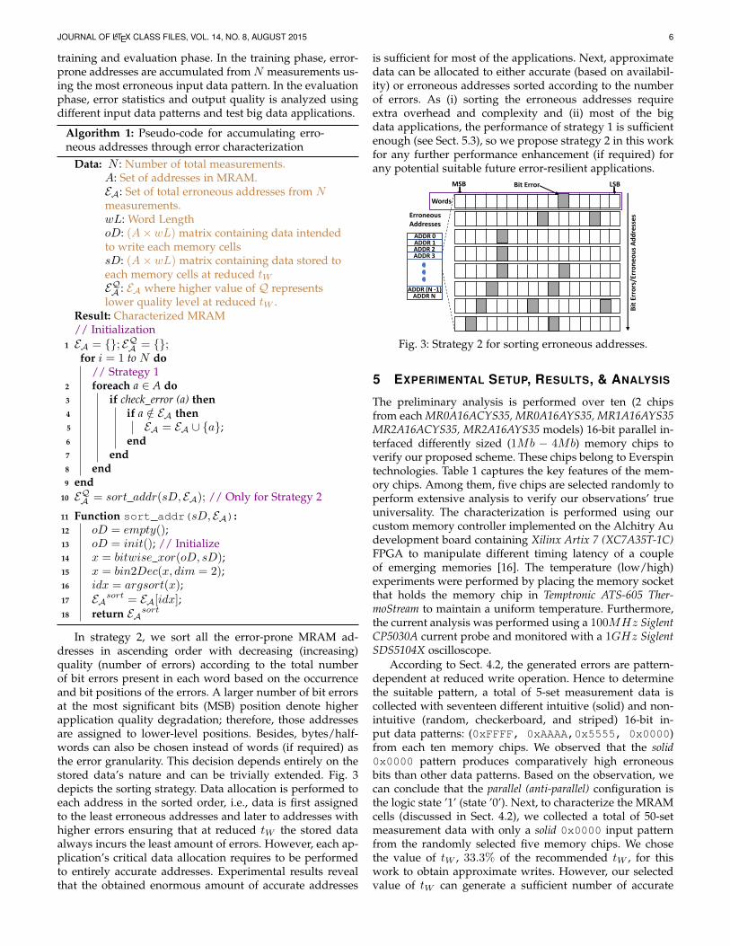
In strategy 2, we sort all the error-prone MRAM ad-dresses in ascending order with decreasing (increasing)quality (number of errors) according to the total numberof bit errors present in each word based on the occurrenceand bit positions of the errors. A larger number of bit errorsat the most significant bits (MSB) position denote higherapplication quality degradation; therefore, those addressesare assigned to lower-level positions. Besides, bytes/half-words can also be chosen instead of words (if required) asthe error granularity. This decision depends entirely on thestored data’s nature and can be trivially extended. Fig. 3depicts the sorting strategy. Data allocation is performed toeach address in the sorted order, i.e., data is first assignedto the least erroneous addresses and later to addresses withhigher errors ensuring that at reduced tW the stored dataalways incurs the least amount of errors. However, each ap-plication’s critical data allocation requires to be performedto entirely accurate addresses. Experimental results revealthat the obtained enormous amount of accurate addresses
is sufficient for most of the applications. Next, approximatedata can be allocated to either accurate (based on availabil-ity) or erroneous addresses sorted according to the numberof errors. As (i) sorting the erroneous addresses requireextra overhead and complexity and (ii) most of the bigdata applications, the performance of strategy 1 is sufficientenough (see Sect. 5.3), so we propose strategy 2 in this workfor any further performance enhancement (if required) forany potential suitable future error-resilient applications.
ADDR 0ADDR 1ADDR 2ADDR 3
ADDR (N -1)ADDR N
LSBMSB
Erroneous Addresses
Words
Bit Error
Bit
Err
ors
/Err
on
eo
us
Ad
dre
sse
s
Fig. 3: Strategy 2 for sorting erroneous addresses.
5 EXPERIMENTAL SETUP, RESULTS, & ANALYSIS
The preliminary analysis is performed over ten (2 chipsfrom each MR0A16ACYS35, MR0A16AYS35, MR1A16AYS35MR2A16ACYS35, MR2A16AYS35 models) 16-bit parallel in-terfaced differently sized (1Mb − 4Mb) memory chips toverify our proposed scheme. These chips belong to Everspintechnologies. Table 1 captures the key features of the mem-ory chips. Among them, five chips are selected randomly toperform extensive analysis to verify our observations’ trueuniversality. The characterization is performed using ourcustom memory controller implemented on the Alchitry Audevelopment board containing Xilinx Artix 7 (XC7A35T-1C)FPGA to manipulate different timing latency of a coupleof emerging memories [16]. The temperature (low/high)experiments were performed by placing the memory socketthat holds the memory chip in Temptronic ATS-605 Ther-moStream to maintain a uniform temperature. Furthermore,the current analysis was performed using a 100MHz SiglentCP5030A current probe and monitored with a 1GHz SiglentSDS5104X oscilloscope.
According to Sect. 4.2, the generated errors are pattern-dependent at reduced write operation. Hence to determinethe suitable pattern, a total of 5-set measurement data iscollected with seventeen different intuitive (solid) and non-intuitive (random, checkerboard, and striped) 16-bit in-put data patterns: (0xFFFF, 0xAAAA,0x5555, 0x0000)from each ten memory chips. We observed that the solid0x0000 pattern produces comparatively high erroneousbits than other data patterns. Based on the observation, wecan conclude that the parallel (anti-parallel) configuration isthe logic state ’1’ (state ’0’). Next, to characterize the MRAMcells (discussed in Sect. 4.2), we collected a total of 50-setmeasurement data with only a solid 0x0000 input patternfrom the randomly selected five memory chips. We chosethe value of tW , 33.3% of the recommended tW , for thiswork to obtain approximate writes. However, our selectedvalue of tW can generate a sufficient number of accurate
JOURNAL OF LATEX CLASS FILES, VOL. 14, NO. 8, AUGUST 2015 7
TABLE 1: MRAM Chip Specifications [15].Parameter Standard Value
Capacity, Supply Voltage 1 - 4 Mbit, 3.3 V
Read/Write Cycle (tWC ) 35 ns
Write Pulse Width (tW ) 15 nsWrite Recovery Time (tWR) 12 ns
Valid Data to end of Write (tDV ) 10 nsAddress/Data Bus Length 16 - 18/16Retention Time >20 years
AC stand by Current 18–28 mA
AC Active Current (Read/Write) 55–80 mA/105–165 mA
addresses (moderate number of incorrect outputs) for theproposed framework.
Analyzing results from the conducted experiments vali-date our proposed scheme’s novelty and provide interestinginsights. The results are divided into four broad subsections.In the first part, we manifest the quality (number of erro-neous cells/addresses) power (write current) trade-off forselecting the reduced tW appropriately, a universal trait inany approximate computing mechanism. The second partpresents the characterization results in detail applying Algo.1. The third part shows how the output quality is affectedwhen data is written into the memory with different ini-tialized values and with or without applying the proposedaddress selection strategy (strategy 1 of Algo. 1). We alsoshow that our approach results in significantly higher powersavings than many popular (non) volatile memory-basedprior works [8], [9], [10], [12]. Moreover, an efficient imple-mentation of a memory controller can further improve theoverall performance of our proposed framework. Note thatall results presented in the Sects. 5.2 and 5.3 are obtained atroom temperature (26C). Finally, the fourth part describesthe results obtained using the approximate MRAM subjectto environmental and memory chip variations.
5.1 Selection of tW
An extensive analysis is performed to determine the er-ror profile, such as frequency, location of the bit errors,comparing the behavior of the faulty/erroneous outputsat different reduced tW values using solid 0x0000 datapattern. We reduce the tW value from 15ns (manufacturer’srecommended) to 10ns, 5ns, and 2.5ns, respectively. Dueto the experimental setup limitations, we are incapable ofreducing the tW value any further. At tW = 2.5ns, the totalnumber of failed bit count falls within 25.59% − 37.30%,which is sufficient for TRNG or PUF analysis [35] but notsuitable for data approximation. However, at tW = 5ns and10ns, the obtained total failed bits are almost negligible(< 5% and < 1%, respectively) for all ten chips. Hence,we choose tW = 5ns (considering the number of failed bitcounts) to characterize erroneous cells to notably enhancesystem performance and power savings. Fig. 5 portraysthe write current observed in different tW values. It showsthat a suitable decrease in tW decreases notable powerconsumption by maintaining a sufficient number (see Table2) of accurate addresses (and hence output quality).
5.2 Characterization of Error-Prone CellsThe cell characterization of MRAM is performed accordingto Sect. 4.2 with N = 50 temporal measurements. Solid0x0000 is used as the write data pattern. Moreover, theentire memory is reset with the solid 0xFFFF data patternbefore every measurement to erase the trace of previouslywritten data. In Table 2, the first two rows show the statisticsof erroneous MRAM addresses and bits after performingthe proposed cell characterization algorithm (strategy 1 ofAlgo. 1). Here, EA(EB)is the percentage of total erroneousaddresses (bits) from 50 temporal measurements (obtainedthrough characterization). The results manifest that the totalnumber of erroneous bits obtained at reduced tW (2.5ns)varies from chip to chip. Besides, only a few addresseshold these erroneous bits. The rest of the rows representerroneous addresses (bits) from different data patterns andto which extent they belong to EA(EB). Here, MA(MB)is the percentage of total erroneous addresses (bits) froma specific data pattern, and CA(CB) is the percentage ofMA(MB) belongs to EA(EB).
We observe that the maximum erroneous addresses(bits) range from different memory chips are only[5.33%, 26.41%] ([3.89%, 22.06%]) after performing char-acterization at tW = 5ns. This indicates that ∼75% (∼78%)of the addresses (bits) are entirely accurate, resulting innegligible or no loss in output quality. As the percentageof erroneous addresses is fairly small (∼25%) regardless ofmemory size, storage overhead is minimal for storing thesefew memory addresses’ information.
For pattern 0xAAAA or 0x5555, we do not observe anyerror for any data pattern. Base on the internal architectureof MRAM, there might be different reasons behind notgetting any error. For example, if all of the I/O buffers aredriven by the same power rail, the inrush current causedby the I/O buffers should be lower for these specific datapatterns as only 8 out of 16 bits experience the switch-ing [37]. Hence, the overall timing characteristics mightbe improved [37]. Moreover, the obtained erroneous ad-dresses, MA (bits, MB) in reduced tW are in the range[0.16%, 6.04%] ([0.08%, 3.30%]) for any other data pat-terns considering all memory chips, while most of thesebelong/close to the lower limit. Besides, our proposed char-acterization technique covers most erroneous addresses, CA(bits, CB) for all data patterns. Although the lowest cov-ered erroneous addresses, CA (bits, CB) is 1.74% (2.76%)for the solid 0xFFFF data pattern; however, a closer ob-servation reveals that solid 0xFFFF data pattern producesonly 0.26% (0.23%) error addresses (bits) which itself isnegligible (< 0.5%). This insignificant number of errors canbe overlooked for any big data application.
5.3 EvaluationWe use the most common and popular metrics, signal-to-noise ratio (SNR) and mean squared error (MSE), betweenthe approximated image and the original image to evaluateand measure the acceptability of the application outputquality. The SNR and MSE are calculated using the follow-ing equations (Eqs. 1 and 2) based on the original image,f(i, j), and the approximated image, f(i, j), obtained afterperforming the proposed approximate framework. Notethat the size of the images is M ×N .

JOURNAL OF LATEX CLASS FILES, VOL. 14, NO. 8, AUGUST 2015 8
TABLE 2: Error Characteristics.Sample Chip1 (%) C1 C2 C3 C4 C5
Characterization EA 22.41 26.41 10.34 8.36 5.33EB 10.49 22.06 7.60 5.15 3.89
Solid
FFFF
MA 0.26 0.26 0 0 0MB 0.11 0.23 0 0 0CA 1.74 60.81 —- —- —-CB 2.76 54.39 —- —- —-
0000
MA 2.52 6.04 1.83 2.04 1.29MB 0.83 3.30 1.25 1.36 0.86CA 96.92 99.28 95.26 86.23 94.34CB 85.48 98.36 94.37 80.73 91.5
RowStriped
FFFF
MA 1.99 3.52 0.72 0.82 0.62MB 0.67 2.13 0.53 0.56 0.47CA 97.78 99.55 95.2 92.87 95.78CB 90.9 98.34 94.42 91.43 94.11
0000
MA 0.75 2.63 0.94 1.09 0.67MB 0.18 1.25 0.61 0.68 0.40CA 97.77 99.45 96.8 84.29 94.03CB 83.07 98.55 96.02 76.87 90.46
ColumnStriped
FFFF
MA 1.68 0 1.06 1.27 0.89MB 0.67 0 0.71 0.79 0.60CA 87.4 — 93.13 90.23 89.82CB 74.8 — 92.75 89.73 88.73
0000
MA 1.37 1.18 0.32 0.37 0.22MB 0.54 0.94 0.19 0.20 0.12CA 46.99 90.73 51.74 32.89 34.93CB 47.51 93.23 51.25 29.09 35.42
Checker-board
FFFF
MA 1.59 3.05 0.71 0.84 0.61MB 0.60 1.77 0.51 0.53 0.41CA 76.3 96.02 83.44 74.97 79.47CB 68.07 93.81 83.96 76.62 80.64
0000
MA 1.25 2.96 0.64 0.75 0.49MB 0.59 1.55 0.40 0.42 0.29CA 62.61 96.02 85.71 83.54 81.54CB 60.43 93.62 83.97 82.49 79.89
AnyPattern2
5555 /AAAA
MA 0 0 0 0 0MB 0 0 0 0 0CA —- —- —- — —CB —- —- —- — —
Random
MA 0.27 0.28 0.22 0.19 0.16MB 0.13 0.13 0.11 0.42 0.08CA 34.83 68.94 13.97 10.18 10.12CB 20.99 62.47 11.5 7.55 8.02
∗NB. —- not performed as no error occurred at reduced tW forcorresponding data patterns.
SNR =
∑Mi=1
∑Nj=1 f(i, j)2∑M
i=1
∑Nj=1[f(i, j)− f(i, j)]2
(1)
MSE =1
MN
M∑i=1
N∑j=1
[f(i, j)− f(i, j)]2 (2)
The value of SNR and MSE measures the image’s qualityin image processing applications, evaluating the proposedscheme’s effectiveness. A minimum SNR value is requiredfor such applications for the approximated image wherethe human brain and eyes can differentiate between theapproximated and original image. A lower (higher) SNR(MSE) value is considered as unacceptable output qualityand vice versa. The SNR and MSE measurements revealthe degree to which an application could produce satisfac-tory and reasonable output at reduced tW for approximateapplications and determine the achievable limits of the
1. C1: MR0A16AYS35, C2: MR1A16AYS35, C3&C4: MR2A16ACYS35,C5: MR2A16AYS35. C1,C2&C5: Commercial Grade (Temp. range[0C, 70C]); C3&C4: Industrial Grade (Temp. range [−40C, 85C]).
2. Solid/ Striped/ Checkerboard.
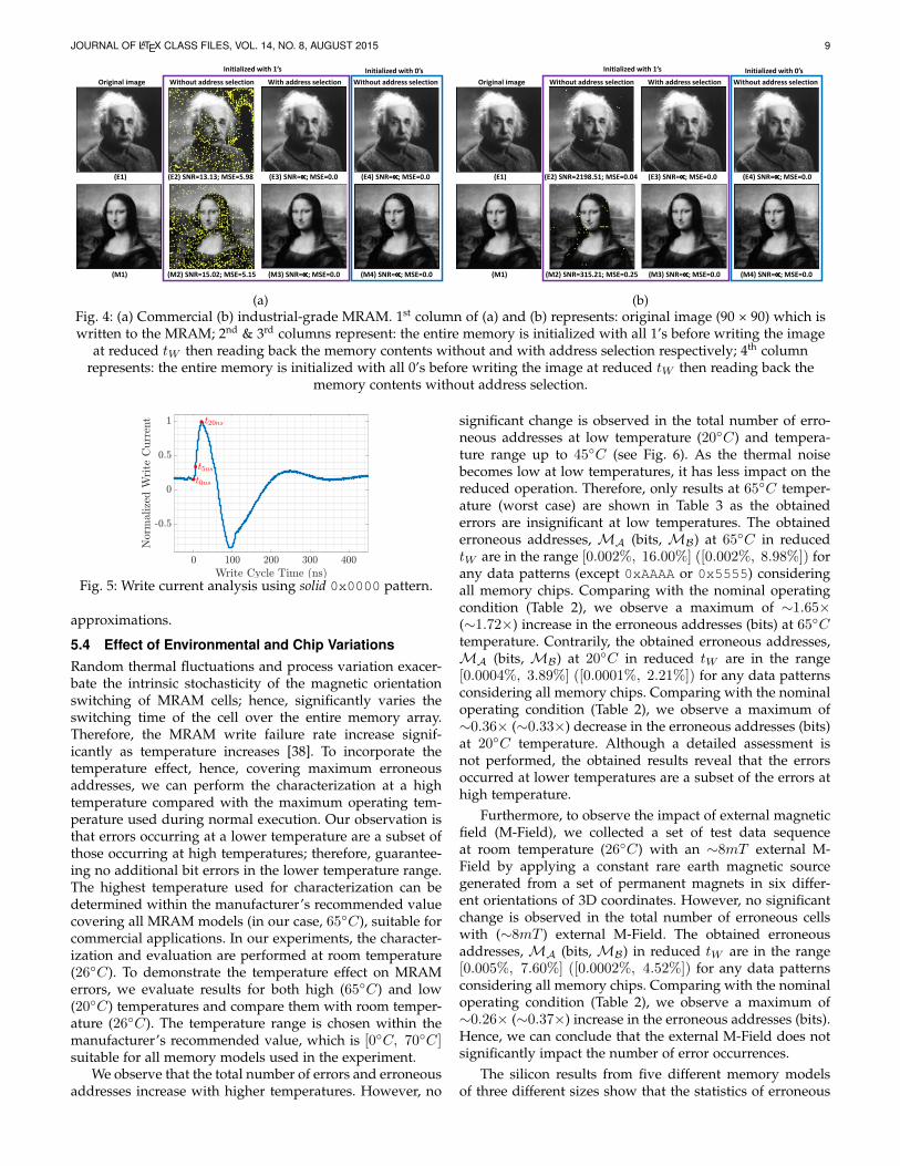
performance and power improvements for MRAM tech-nology. Fig. 4 shows the original and approximate outputimage quality (represented quantitatively by SNR and MSE)with and without applying the proposed addresses selectiontechnique (strategy 1 of Algo. 1), considering two differentinitialization states. The SNR (MSE) of the image is infinite(zero) means it does not have any errors relative to theoriginal image output. Observing the images and the relatedSNR and MSE reveals the appropriateness of the proposedtechnique through improved application quality. Note thatthe test image pixels are allocated in entirety to each of therequired memory addresses.
Moreover, we evaluate the effectiveness of applying theaddress selection technique. The results depict the influ-ence of address selection on application quality, which isnecessary to understand the impact of approximate dataplacement in memory addresses. This, in turn, is useful tocomprehend how application quality changes with initial-ized values. In Fig. 4, the 2nd & 3rd columns show the read-back image without and with applying the address selectiontechnique, respectively. It is evident that the image qualityimprovement obtained using the proposed address selectiontechnique is substantially better than without applying thetechnique, underscoring the need for the proposed addressselection. However, as switching from ’1‘ → ’0‘ is morevulnerable at reduced tW , requiring more write currentfor the prolonged duration; hence, initializing the entirememory with all 1’s requires address selection techniqueto attain negligible or no loss in the output quality. Con-trarily, initializing the entire memory with all 0’s does notrequire an address selection technique to obtain the samelevel of output quality. Furthermore, we also observe thatcommercial-grade MRAM is more vulnerable to reducedtW than industrial-grade MRAM due to internal MRAMarchitecture. Therefore, without applying the address se-lection technique in industrial-grade MRAMs, we notice anegligible loss in the output quality.
We next present the result that demonstrates the ob-tained power efficiency. To measure the write current, hence,power, we use a current probe and oscilloscope. However,the analog bandwidth of the current probe is 100MHz;hence, the resolution of the current probe is greater than10ns. Therefore, we are incapable of measuring the accuratewrite current at reduced tW = 5ns. Due to the absenceof proper equipment, we relied on the measurement sup-ported by our current probe to measure the write currentconcerning a prolonged write cycle time (60ns > standard15ns). Fig. 5 portrays the write current analysis for the solid0x0000 pattern, which produces the maximum numberof errors in the reduced write operation. The 1st half ofthe signal shows the consumed current during the writeoperation, and the 2nd half shows the discharge current.Here the normalized current values at points t0ns, t5ns, andt20ns are 0, 0.34, and 1, respectively. The temporal distancebetween points t0ns and t5ns is 5ns (reduced tW used in ourproposed scheme), and t0ns and t20ns is 20ns (> standardtW = 15ns for COTS MRAM). As p ∝ i2, where p = powerand i = current, hence the obtained power reduction ispred = (12−0.342)
12 = 0.88, illustrating the effectiveness ofthe proposed framework to achieve power benefits through
JOURNAL OF LATEX CLASS FILES, VOL. 14, NO. 8, AUGUST 2015 9
Original image Without address selection With address selection Without address selection
(E1) (E2) SNR=13.13; MSE=5.98 (E3) SNR≈∝; MSE=0.0 (E4) SNR=∝; MSE=0.0
(M1) (M2) SNR=15.02; MSE=5.15 (M3) SNR≈∝; MSE=0.0 (M4) SNR≈∝; MSE=0.0
Initialized with 1’s Initialized with 0’s
(a)
Original image Without address selection With address selection Without address selection
(E1) (E2) SNR=2198.51; MSE=0.04 (E3) SNR≈∝; MSE=0.0 (E4) SNR=∝; MSE=0.0
(M1) (M2) SNR=315.21; MSE=0.25 (M3) SNR≈∝; MSE=0.0 (M4) SNR≈∝; MSE=0.0
Initialized with 1’s Initialized with 0’s
(b)Fig. 4: (a) Commercial (b) industrial-grade MRAM. 1st column of (a) and (b) represents: original image (90 × 90) which iswritten to the MRAM; 2nd & 3rd columns represent: the entire memory is initialized with all 1’s before writing the image
at reduced tW then reading back the memory contents without and with address selection respectively; 4th columnrepresents: the entire memory is initialized with all 0’s before writing the image at reduced tW then reading back the
memory contents without address selection.
Fig. 5: Write current analysis using solid 0x0000 pattern.
approximations.
5.4 Effect of Environmental and Chip VariationsRandom thermal fluctuations and process variation exacer-bate the intrinsic stochasticity of the magnetic orientationswitching of MRAM cells; hence, significantly varies theswitching time of the cell over the entire memory array.Therefore, the MRAM write failure rate increase signif-icantly as temperature increases [38]. To incorporate thetemperature effect, hence, covering maximum erroneousaddresses, we can perform the characterization at a hightemperature compared with the maximum operating tem-perature used during normal execution. Our observation isthat errors occurring at a lower temperature are a subset ofthose occurring at high temperatures; therefore, guarantee-ing no additional bit errors in the lower temperature range.The highest temperature used for characterization can bedetermined within the manufacturer’s recommended valuecovering all MRAM models (in our case, 65C), suitable forcommercial applications. In our experiments, the character-ization and evaluation are performed at room temperature(26C). To demonstrate the temperature effect on MRAMerrors, we evaluate results for both high (65C) and low(20C) temperatures and compare them with room temper-ature (26C). The temperature range is chosen within themanufacturer’s recommended value, which is [0C, 70C]suitable for all memory models used in the experiment.
We observe that the total number of errors and erroneousaddresses increase with higher temperatures. However, no
significant change is observed in the total number of erro-neous addresses at low temperature (20C) and tempera-ture range up to 45C (see Fig. 6). As the thermal noisebecomes low at low temperatures, it has less impact on thereduced operation. Therefore, only results at 65C temper-ature (worst case) are shown in Table 3 as the obtainederrors are insignificant at low temperatures. The obtainederroneous addresses, MA (bits, MB) at 65C in reducedtW are in the range [0.002%, 16.00%] ([0.002%, 8.98%]) forany data patterns (except 0xAAAA or 0x5555) consideringall memory chips. Comparing with the nominal operatingcondition (Table 2), we observe a maximum of ∼1.65×(∼1.72×) increase in the erroneous addresses (bits) at 65Ctemperature. Contrarily, the obtained erroneous addresses,MA (bits, MB) at 20C in reduced tW are in the range[0.0004%, 3.89%] ([0.0001%, 2.21%]) for any data patternsconsidering all memory chips. Comparing with the nominaloperating condition (Table 2), we observe a maximum of∼0.36× (∼0.33×) decrease in the erroneous addresses (bits)at 20C temperature. Although a detailed assessment isnot performed, the obtained results reveal that the errorsoccurred at lower temperatures are a subset of the errors athigh temperature.
Furthermore, to observe the impact of external magneticfield (M-Field), we collected a set of test data sequenceat room temperature (26C) with an ∼8mT external M-Field by applying a constant rare earth magnetic sourcegenerated from a set of permanent magnets in six differ-ent orientations of 3D coordinates. However, no significantchange is observed in the total number of erroneous cellswith (∼8mT ) external M-Field. The obtained erroneousaddresses, MA (bits, MB) in reduced tW are in the range[0.005%, 7.60%] ([0.0002%, 4.52%]) for any data patternsconsidering all memory chips. Comparing with the nominaloperating condition (Table 2), we observe a maximum of∼0.26× (∼0.37×) increase in the erroneous addresses (bits).Hence, we can conclude that the external M-Field does notsignificantly impact the number of error occurrences.
The silicon results from five different memory modelsof three different sizes show that the statistics of erroneous

JOURNAL OF LATEX CLASS FILES, VOL. 14, NO. 8, AUGUST 2015 10
cells are different for different memory models, shown inTables 2 and 3. These sources of variations come fromarchitectural as well as both inter- and intra-chip dissimi-larities due to the random process variation, which is thekey source of any memory chips’ randomness. Furthermore,data collected from different FPGAs verify that the memorycontrollers do not influence the proposed framework.
TABLE 3: Error Statistics at High Temperature.Sample Chip (%) C1 C2 C3 C4 C5
Solid
FFFF
MA 0.002 0.09 0 0 0MB 0.002 0.02 0 0 0CA 100 5.79 —- —- —-CB 100 16.77 —- —- —-
0000
MA 16.00 13.53 7.55 2.73 0.94MB 6.31 7.54 4.30 0.56 0.22CA 39.70 77.63 10.72 11.77 21.8CB 26.59 74.68 7.93 17.07 32.54
RowStriped
FFFF
MA 12.83 6.92 4.63 1.61 0.33MB 6.05 3.87 1.85 0.35 0.12CA 47.39 81.38 13.84 15.64 38.17CB 32.07 79.25 13.31 21.56 42.08
0000
MA 12.79 5.74 2.87 1.01 0.167MB 5.61 3.07 1.33 0.21 0.07CA 30.32 78.44 6.74 5.91 14.65CB 18.65 73.35 3.11 9.61 22.77
ColumnStriped
FFFF
MA 15.56 9.93 3.55 1.02 0.273MB 8.98 5.41 1.04 0.24 0.12CA 47.66 74.21 12.32 16.07 48.42CB 27.41 68.75 15.01 23.16 53.61
0000
MA 3.15 2.13 2.55 0.83 0.23MB 0.76 0.93 0.68 0.15 0.09CA 28.25 95.81 9.32 14.93 36.38CB 41.57 94.11 14.83 23.5 37.36
Checker-board
FFFF
MA 9.40 5.93 3.34 0.84 0.23MB 4.75 3.21 0.86 0.20 0.11CA 50.53 80.52 12.11 17.01 48.17CB 33.8 75.31 16.94 26.46 53.5
0000
MA 9.10 5.96 3.37 0.89 0.25MB 4.37 3.06 0.93 0.19 0.11CA 40.51 78.21 8.82 14.67 41.71CB 24.48 71.84 12.77 22.76 41.62
AnyPattern
5555/AAAA
MA 0 0 0 0 0MB 0 0 0 0 0CA —- —- —- —- —-CB —- —- —- —- —-
Random
MA 0.13 0.23 0.01 0.005 0.008MB 0.04 0.09 0.01 0.002 0.002CA 59.09 72.97 31.43 38.46 38.1CB 33.16 63.81 36.3 40.48 41.58
∗NB. —- not performed as no error occurred at reduced tW forcorresponding data patterns.
5.5 Data Pattern Dependency
The characterization analysis was also performed with intu-itive, such as solid and non-intuitive data patterns such ascheckerboard, striped, and random to consider the effect ofdata pattern dependency. Taking the union of the errors re-sulting from each data pattern can further improve the faultcoverage during the worst case. However, only a marginalimprovement is observed for the chips used for experimentsusing different data patterns over the solid 0x0000 datapattern. Besides, Table 2 shows that a vast portion of theerroneous addresses generated from different data patternsbelongs to those erroneous addresses obtained through theaddress selection strategy from error characterization usingsolid 0x0000 data pattern described in strategy 1 of Algo.1. Furthermore, it is essential to note that the acquirederroneous addresses heavily depend on the training data
and frequency characteristics. Hence, it becomes imperativeto select the training data and frequency judiciously.
5.6 Summary of ResultsOverall, we draw the following main conclusions from theresults.
1) The reduction of the MRAM chip’s write pulse width(tW ) can be used to achieve maximum write currentsavings of ∼66% (hence, power-saving of ∼88%)with virtually no loss in output quality for error-resilient applications.
2) The cell characterization is performed once in a life-time before deploying the MRAM in the computingsystem. However, the judicial selection is requiredfor the training data and frequency to perform char-acterization.
3) The output quality degradation occurs when ap-proximate application data are placed at addressescontaining both erroneous and error-free (withoutaddress selection) due to the bit errors present inerroneous addresses in the case when the entirememory initialized with all 1’s before writing. How-ever, with the proposed address selection strategy,we can achieve almost 100% of output quality.
4) Contrarily, the same applications retain almost100% of quality even when put into addresses con-taining both erroneous and error-free in the casewhen the entire memory initialized with all 0’sbefore writing.
5) Commercial-grade MRAM is more vulnerable toreduced tW than industrial-grade MRAM due tointernal MRAM architecture.
6) Errors that occurred at lower temperatures are asubset of the errors at high temperatures.
6 DISCUSSIONS
6.1 Storage and Performance OverheadsOur proposed framework requires allocating applicationdata (critical and then approximate) to first error-free ad-dresses and move forward to erroneous addresses basedon the required application accuracy. We used a similarapproach proposed in [10]; however, our approach is sim-pler as the access policy of DRAM and MRAM is entirelydifferent, and we do not require quality-wise erroneousaddress sorting. Note that the following strategy needs tobe performed only for high-accuracy applications when nomore accurate addresses are available. For this purpose, acustom memory allocator is required to track the erroneousaddresses obtained from the characterization step. Next,based on the application requirements, it will allocate theuser annotated critical and approximate data into virtualaddresses using a critical bit for each address. Operatingsystems (OS) usually accomplish the mapping of virtualto physical addresses through a page table. Hence, in ourproposed scenario, the OS has to perform this additionalresponsibility of assigning virtual to physical addressesbelonging to error-free (accurate) and erroneous addressesdepending on the application requirement.
The OS and the memory management unit (MMU) re-quire additional logic to implement the proposed addressesselection strategy. Towards this end, first, the OS can track

JOURNAL OF LATEX CLASS FILES, VOL. 14, NO. 8, AUGUST 2015 11
Original image Without address selection With address selection
(E1) (E2) SNR=13.43; MSE=5.84 (E3) SNR≈∝; MSE=0.0
(M1) (M2) SNR=14.52; MSE=5.29 (M3) SNR≈∝; MSE=0.0
Initialized with 1’s
(a)
Original image Without address selection With address selection
(E1) (E2) SNR=943.34; MSE=0.09 (E3) SNR≈∝; MSE=0.0
(M1) (M2) SNR=346.55; MSE=0.23 (M3) SNR≈∝; MSE=0.0
Initialized with 1’s
(b)Fig. 6: (a) Commercial (b) industrial-grade MRAM. 1st column of (a) and (b) represents the original image (90 × 90)
which is written to the MRAM; 2nd & 3rd columns represent: the entire memory is initialized with all 1’s beforewriting the image at reduced tW then reading back the memory contents without and with address selection
respectively at 45C3
the erroneous addresses using a custom data structure (con-sisting of critical bits). Then, at the start-up phase, the OScan utilize the custom data structure to modify the core mapand subsequently utilize this modified mapping functionto translate virtual to a physical address. Note that themodified mapping is used in conjunction with the originalcore map. Before performing virtual to physical addressmapping, first, the OS will check whether the virtual addressis critical or not for the required application. If it is critical,the OS will check for the error-free address based on theapplication requirement as specified by the system designer.In addition to that, one can use additional flag bits on thecache memory (similar to the valid bit) to identify if a datablock is erroneous or accurate. This flag bit can be directlycopied from the custom data structure in parallel to the mainmemory operations. The OS can utilize this flag bit duringthe memory allocation for further optimization. For the pro-posed framework, it is expected that the OS will completelyautomate the entire allocation process. Hence, hardware andOS support are essential for adapting approximate MRAMto reality in sophisticated high-end embedded computingsystems. Note that, for a 1GByte main memory (with 32Byteblock size), the size of the custom data structure would be4MByte. It is worth mentioning that the latency and energyoverheads for the MRAM characterization are negligible asthe characterization needs to be performed only once beforedeploying the MRAM in the computing system.
6.2 Critical Data Protection: MRAM as a Cache
A significant challenge of approximate storage usage is:most of the highly amenable approximate computingparadigm applications also have a mixture of control data(i.e., critical data) that is intolerable to any errors. Henceimposing approximation on these data makes them unre-liable. For example, the instruction cache requires to beentirely error-free. Various solutions are proposed to protect
3. While working on the image experiment, we do not have accessto the mentioned ThermoStream; hence unable to reach 65C (usedfor characterization). In the revised version, we are planning to showimage results at 65C.
the critical data part [8]. The critical data size is minimalcomparing with the non-critical counterpart. Hence, design-ing a heterogeneous data cache memory array with differentstatic (design-time) and dynamic (runtime) configurationsto make critical data error-resilient guarantees error-freeoperation. However, this requires (i) fabrication parametersmodification (ii) complex cache controller for proper dataallocation in different arrays. Contrarily, a more straight-forward solution for critical data protection is either usingmultiple copies of this data content or an error correctioncode (ECC), where data protection is performed throughadditional check bit(s). However, the overhead due to theadditional bit-cells for the mentioned approaches is minimalfor these significantly smaller critical data sizes [8]. Besides,considerably lower write accesses to the instruction cachehelp the critical data protection considerably more manage-able for our proposed framework.
7 CONCLUSION
This paper proposes an efficient approximate computingframework to evaluate the applicability of non-volatileCOTS MRAM, a promising candidate for future computingplatforms, through memory address’s error characterizationby utilizing the internal write latency variation of MRAMto improve the power efficiency. Our methodology pro-vides an optimal system-level implementation yielding afavorable performance and power vs. quality trade-off forerror-resilient applications by devising efficient segregationstrategies for the erroneous addresses allocating approxi-mate and critical data during page mapping systematically.Our experimental results reveal that MRAM-based memorysystem can achieve substantial power and performance ben-efits for negligible or no loss in application output quality.Furthermore, other emerging memory technologies can alsoadopt the proposed address selection strategy, a promisingframework aspect.
REFERENCES
[1] J. A. Mandelman et al., “Challenges and future directions for thescaling of dynamic random-access memory (dram),” IBM Journalof Research and Development, vol. 46, no. 2.3, pp. 187–212, 2002.

JOURNAL OF LATEX CLASS FILES, VOL. 14, NO. 8, AUGUST 2015 12
[2] Q. Xu, T. Mytkowicz, and N. S. Kim, “Approximate computing: Asurvey,” IEEE Design Test, vol. 33, no. 1, pp. 8–22, 2016.
[3] J. Han and M. Orshansky, “Approximate computing: An emergingparadigm for energy-efficient design,” in 2013 18th IEEE EuropeanTest Symposium (ETS), 2013, pp. 1–6.
[4] S. Ghosh et al., “Security and privacy threats to on-chip non-volatile memories and countermeasures,” in Proceedings of the 35thInternational Conference on Computer-Aided Design, 2016.
[5] X. Fong et al., “Spin-transfer torque memories: Devices, circuits,and systems,” Proceedings of the IEEE, vol. 104, no. 7, pp. 1449–1488, 2016.
[6] A. Jog et al., “Cache revive: Architecting volatile stt-ram caches forenhanced performance in cmps,” in Proceedings of the 49th AnnualDesign Automation Conference, 2012, p. 243–252.
[7] X. Wu et al., “Hybrid cache architecture with disparate memorytechnologies,” in Proceedings of the 36th Annual International Sym-posium on Computer Architecture, 2009, p. 34–45.
[8] N. Sayed, R. Bishnoi, and M. B. Tahoori, “Approximate spintronicmemories,” J. Emerg. Technol. Comput. Syst., vol. 16, no. 4, Sep. 2020.
[9] S. Liu, K. Pattabiraman, T. Moscibroda, and B. G. Zorn, “Flikker:Saving dram refresh-power through critical data partitioning,”SIGPLAN Not., vol. 46, no. 3, p. 213–224, Mar. 2011.
[10] A. Raha et al., “Quality configurable approximate dram,” IEEETransactions on Computers, vol. 66, no. 7, pp. 1172–1187, 2017.
[11] I. J. Chang, D. Mohapatra, and K. Roy, “A priority-based 6t/8thybrid sram architecture for aggressive voltage scaling in videoapplications,” IEEE Transactions on Circuits and Systems for VideoTechnology, vol. 21, no. 2, pp. 101–112, 2011.
[12] A. Ranjan et al., “Approximate storage for energy efficient spin-tronic memories,” in 2015 52nd ACM/EDAC/IEEE Design Automa-tion Conference (DAC), 2015, pp. 1–6.
[13] M. Shoushtari, A. BanaiyanMofrad, and N. Dutt, “Exploitingpartially-forgetful memories for approximate computing,” IEEEEmbedded Systems Letters, vol. 7, no. 1, pp. 19–22, 2015.
[14] J. S. Miguel, M. Badr, and N. E. Jerger, “Load value approxima-tion,” in 2014 47th Annual IEEE/ACM International Symposium onMicroarchitecture, 2014, pp. 127–139.
[15] “Everspin 16-bit parallel interface mram,” accessed: 22April 2021. [Online]. Available: https://www.everspin.com/parallel-interface-mram
[16] J. Rajewski, “Alchitry au fpga development board,” accessed: 22April 2021. [Online]. Available: https://alchitry.com/products/alchitry-au-fpga-development-board
[17] Y. Kim et al., “Write-optimized reliable design of stt mram,” inProceedings of the 2012 ACM/IEEE International Symposium on LowPower Electronics and Design, New York, NY, USA, 2012, p. 3–8.
[18] S. Chatterjee et al., “A scalable design methodology for energyminimization of sttram: A circuit and architecture perspective,”IEEE Transactions on Very Large Scale Integration (VLSI) Systems,vol. 19, no. 5, pp. 809–817, 2011.
[19] X. Wu et al., “Hybrid cache architecture with disparate memorytechnologies,” in Proceedings of the 36th Annual International Sym-posium on Computer Architecture, vol. 37, no. 3, New York, NY, USA,Jun. 2009, p. 34–45.
[20] B. Wang et al., “Exploring hybrid memory for gpu energy effi-ciency through software-hardware co-design,” in Proceedings of the22nd International Conference on Parallel Architectures and Compila-tion Techniques, 2013, pp. 93–102.
[21] P. Zhou et al., “Energy reduction for stt-ram using early write ter-mination,” in 2009 IEEE/ACM International Conference on Computer-Aided Design - Digest of Technical Papers, 2009, pp. 264–268.
[22] S. P. Park et al., “Future cache design using stt mrams for improvedenergy efficiency: Devices, circuits and architecture,” in DACDesign Automation Conference 2012, 2012, pp. 492–497.
[23] D. Suzuki, M. Natsui, A. Mochizuki, and T. Hanyu, “Cost-efficientself-terminated write driver for spin-transfer-torque ram andlogic,” IEEE Transactions on Magnetics, vol. 50, no. 11, pp. 1–4, 2014.
[24] Y. Emre et al., “Enhancing the reliability of stt-ram through circuitand system level techniques,” in 2012 IEEE Workshop on SignalProcessing Systems, 2012, pp. 125–130.
[25] H. Naeimi et al., “Sttram scaling and retention failure,” in inteltechnology journal, vol. 17, no. 1, 2013.
[26] A. Driskill-Smith et al., “Latest advances and roadmap for in-planeand perpendicular stt-ram,” in 2011 3rd IEEE International MemoryWorkshop (IMW), 2011, pp. 1–3.
[27] C. W. Smullen et al., “Relaxing non-volatility for fast and energy-efficient stt-ram caches,” in 2011 IEEE 17th International Symposiumon High Performance Computer Architecture, 2011, pp. 50–61.
[28] A. Sampson et al., “Approximate storage in solid-state memories,”in 2013 46th Annual IEEE/ACM International Symposium on Microar-chitecture (MICRO), 2013, pp. 25–36.
[29] D. Apalkov et al., “Magnetoresistive random access memory,”Proceedings of the IEEE, vol. 104, no. 10, pp. 1796–1830, 2016.
[30] “Tmr sensors,” accessed: 22 April 2021. [On-line]. Available: https://product.tdk.com/en/techlibrary/productoverview/tmr-angle-sensors.html
[31] M. Durlam et al., “Toggle mram: A highly-reliable non-volatilememory,” in 2007 International Symposium on VLSI Technology,Systems and Applications (VLSI-TSA), 2007, pp. 1–2.
[32] B. Engel et al., “A 4-mb toggle mram based on a novel bit andswitching method,” IEEE Transactions on Magnetics, vol. 41, no. 1,pp. 132–136, 2005.
[33] S. Kumar and P. K. Singh, “An overview of modern cache memoryand performance analysis of replacement policies,” in 2016 IEEEInternational Conference on Engineering and Technology (ICETECH),2016, pp. 210–214.
[34] J. L. Hennessy and D. A. Patterson, Computer architecture: a quanti-tative approach. Elsevier, 2011.
[35] F. Ferdaus et al., “True random number generation using latencyvariations of commercial mram chips,” in 2021 22nd InternationalSymposium on Quality Electronic Design (ISQED), 2021, pp. 510–515.
[36] R. Bishnoi et al., “Avoiding unnecessary write operations in stt-mram for low power implementation,” in Fifteenth InternationalSymposium on Quality Electronic Design, 2014, pp. 548–553.
[37] K. Shi and J. Li, “A wakeup rush current and charge-up timeanalysis method for programmable power-gating designs,” in2007 IEEE International SOC Conference, 2007, pp. 163–165.
[38] F. Ferdaus and M. T. Rahman, Security of Emerging Memory Chips.Cham: Springer International Publishing, 2021, pp. 357–390.
Farah Ferdaus (S’20) received her M.S. de-gree in Electrical and Computer Engineeringfrom the University of New Hampshire in 2018.She is currently working towards her Ph.D. inElectrical and Computer Engineering at FloridaInternational University. Her research interestsinclude performance enhancement and securitysolutions of emerging memories; privacy andsecurity issues of existing memories; wirelesscommunications and networks.
B. M. S. Bahar Talukder (S’18) is a Ph.D.student in Electrical and Computer Engineeringat Florida International University. He receivedhis Bachelor’s degree from Bangladesh Uni-versity of Engineering and Technology, Dhaka,Bangladesh. His primary research interests in-clude hardware security, secured computer ar-chitecture, machine-learning application in sys-tem security, and emerging memory technolo-gies.
Md Tauhidur Rahman (S’12–M’18) is an Assis-tant Professor in the Department of Electricaland Computer Engineering at Florida Interna-tional University (FIU). Before joining FIU, hewas an Assistant Professor at the University ofAlabama in Huntsville (UAH). He received hisPh.D. degree in Computer Engineering from theUniversity of Florida in 2017. His current re-search interests include hardware security andtrust, memory system, machine learning appli-cations, embedded security, and reliability.