Embed Size (px)
Citation preview

Jonathan Mitchell 996069032 Stark Industries Application Note SPI, Talking to Chips, and Minimizing Noise How do you communicate with a piece of silicon? How do you communicate with a semiconductor. SPI is a method of communication that allows users to interact with a piece of silicon. You can change certain chip parameters The goal of this tutorial is to teach students how to communicate with a semiconductor in the most efficient manner. Normally, when we add components to a system we increase the overall noise. After this tutorial students should be able to communicate with their chip in order to turn on specific parameters without adding noise to the overall system. Lets get started with a few definitions. SPI stands for Serial Peripheral Interface. It is a synchronous communication method used for short distance communication in embedded systems. Synchronous communication means that your signal is sent in sync (at the same time) as your clock pulse. Here are the components for SPI:
Fig 1. In this case, the pink block labeled SPI Master is the microcontroller and the block labeled SPI Slave is your chip. From now on we will refer to the chip (your semiconductor) as slave, and your microcontroller as Master. SCLK: Serial Clock, because our data is synchronous our data is transmitted in accordance with these clock pulses. This is not Master Clock. MOSI: Master output slave input: This is the master line used for sending data to the peripherals. MISO: Master input slave output: The slave line for sending data to the master. SS: Slave Select. Please note that there is no convention for this term, and it might be noted as CS (Chip Select) throughout this tutorial.
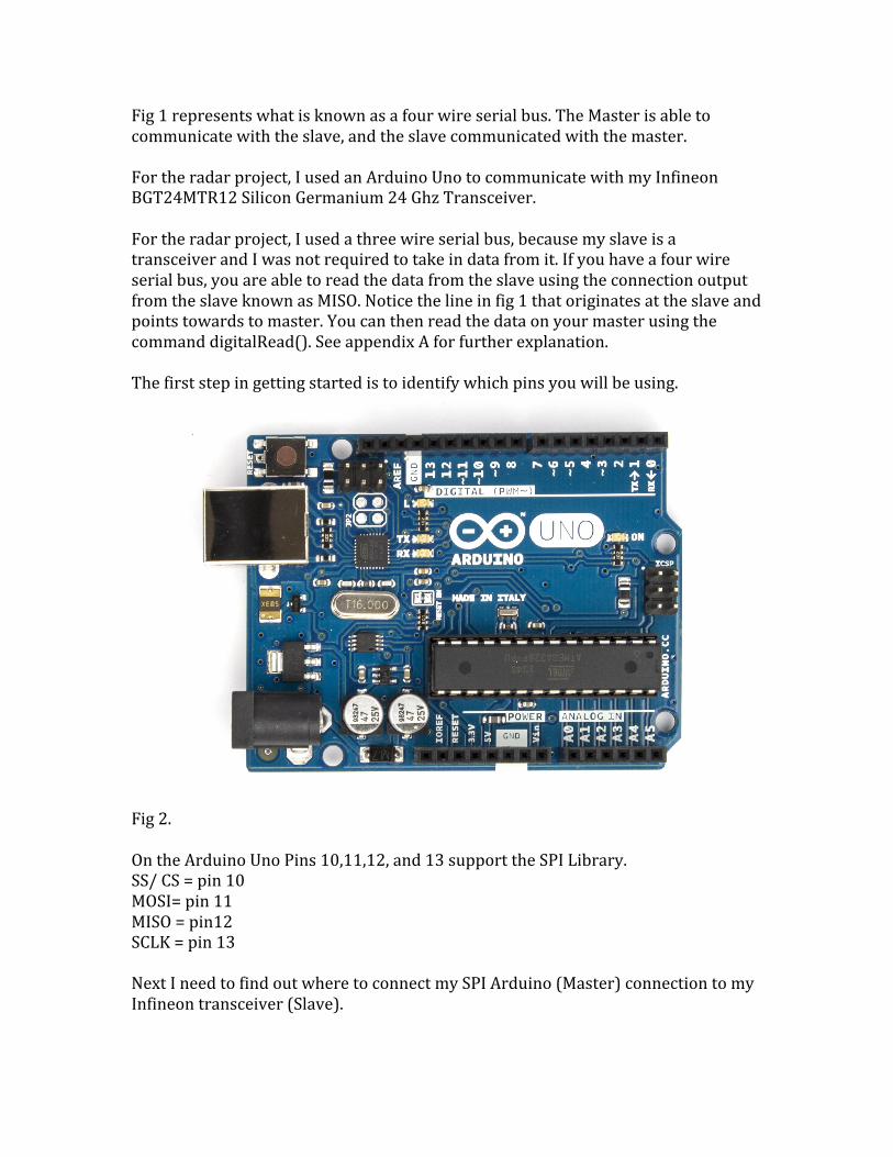
Fig 1 represents what is known as a four wire serial bus. The Master is able to communicate with the slave, and the slave communicated with the master. For the radar project, I used an Arduino Uno to communicate with my Infineon BGT24MTR12 Silicon Germanium 24 Ghz Transceiver. For the radar project, I used a three wire serial bus, because my slave is a transceiver and I was not required to take in data from it. If you have a four wire serial bus, you are able to read the data from the slave using the connection output from the slave known as MISO. Notice the line in fig 1 that originates at the slave and points towards to master. You can then read the data on your master using the command digitalRead(). See appendix A for further explanation. The first step in getting started is to identify which pins you will be using.
Fig 2. On the Arduino Uno Pins 10,11,12, and 13 support the SPI Library. SS/ CS = pin 10 MOSI= pin 11 MISO = pin12 SCLK = pin 13 Next I need to find out where to connect my SPI Arduino (Master) connection to my Infineon transceiver (Slave).

Fig 3. Infineon (Slave) Circuit Schematic One look at this schematic tells me: SI (Slave Input) = MOSI: Pin 20 CLK = pin 19 CS/SS = Slave Select = pin 18 So now I know exactly how to connect my Master (Arduino) to the Slave (Infineon). Ok so now we understand how to connect them together. Now what exactly do I do?

For this project, my goal was to turn on the power amplifier on my Infineon chip which has to be done through SPI, which would amplify my power and enable stronger transmit output (TX).
fig 4. Block Diagram of Infineon BGT24MTR12

Fig 5. Now comes the fun part. So we can see that in order for me to turn on my Power Amplifier which is located at Data Bit 12, I must send a Low signal to bit 12. In this case, I wanted to maintain all other values and only change bit 12.
Fig 6. Timing Diagram of the SPI

When CS is set to low, the semiconductor knows to look for the data. Then CLK and MOSI send in the data. Once CS is set to high the chip stops looking for the data. For my chip, there is a specific requirement that data needs to be present 20ns before and at least 20ns after the falling edge of the clock signal. Tcs = 20ns. There are two Tcs’s. So the requirement is that my master clock cannot be faster than 100Ghz.
2 𝑃𝑢𝑙𝑠𝑒𝑠2 ∗ 10 ∗ 10^− 9 = 100𝐺ℎ𝑧
I would only face complications at master clock rates faster than 100Ghz. My master clock dictates the timing between each line of code. I need to have a master clock rate slower than 100Ghz so that the time difference between when I sent in bits 15-‐8 and send bits 7-‐0 is smaller larger than 20ns. luckily most microcontrollers cannot have clock rates that high. In my case I set I set my Master clock(Arduino Clock) to 8Mhz. This condition is well satisfied. I do so in the following line: SPI.setClockDivider(SPI_CLOCK_DIV2); //clock set to 8Mhz (Please note for full code see Appendix B). Referring to figure 5: For this chip, I have to send 16 bits, but I can only send 8 bits at a time, starting from the MSB (Most Signicant Bit) to the LSB(Least Significant Bit). Therefore to send 16 bits through I must first send in bits 15-‐8 in one line, and then 7-‐0 in the following line. To do this I must use the command digitalWrite(10,Low). This command allows me to send in a low (0V) pulse from my Master to my Slave, activating the chip. (1) digitalWrite(10,Low) //This activates the chip, by sending my CS pulse low. (2) SPI.transfer(0b00100000); //transfers one byte over SPI bus, sending and receiving (3) SPI.transfer(0b00000111); //this part sends in the second half of the bits to the register as low, bits 7-‐0 (4) digitalWrite(10,HIGH); //put Chip Select back to high to deactivate my chip. SPI.transfer() in (1) activates the Slave Select pin low before the transfer is finished then activates it high after the transfer is complete. So digitalWrite(10, Low) activates CS low at pin 10, which is Chip Select = Slave Low, and digitalWrite(10,High) in (4) activates it high after the transfer is complete.

For an explanation of the use of SPI.transfer(), please look at figure 5, look at bit 15 and notice it is set to low (0) in (2). Then look at bit 14 and notice it is also set to low (0) in (2). The next bit is bit 13 is set to high(1) in (2). The next bit is our Power Amplifier’s bit (bit 12) and to turn it on we set it to 0 in (2). Spi.transfer goes from the MSB to the LSB in that order. After bit 12, we simply set every bit to its corresponding active mode to enable full use of the transceivers functionalities. Please note that the last 111 in (3) is to turn the TX(transmit) power reduction bits 2,1, and 0 on. This method successfully turned on my power amplifier and all necessary components of my transceiver so I am done with SPI right? No not at all. The Master needs to be powered in order to work. If I add more components to the overall system I will also add more noise to the over all system. Added noise would interfere with the system because there is already noise from other components. To power the Arduino I need 5V. I did not have a 5V battery available. I noticed that when I power the Arduino using my laptop, there is added noise from the laptop. When I power the Arduino using a simple power strip, I received noise from the power strip because other things were plugged into the power strip as per usual. In order to reduce noise I put together the following circuit shown in fig 7. In general, when you add components to a system, you also add noise. Added noise would offset the advantage of turning on the power amplifier. We must be able to use the radar system outside, so we will not have an outlet available to us. I need to be able to use batteries to power it.
Fig7.

We have 1.5V available batteries in the lab. Therefore if we put four of them in series we now have 6V. To power the Arduino we are required to have 5V. Therefore I created the following circuit in Fig7. Before I discuss the circuit I would like to mention a few things about noise. In David M. Pozar’s book on Microwave Engineering, he describes noise as “one of the most important considerations when evaluating the performance of wireless systems.” In this case, my goal is to identify and minimize noise values. Each resistor in my circuit has an inherent Thermal Noise associated with it that is caused by random motion of charge carriers. We can use the Rayleigh-‐Jeans approximation to calculate the amount of noise contributed from this voltage divider circuit. Please note that this approximation is only valid up to frequencies in the microwave band. Also it is important to remember that each resistors contributes noise individually and independent of the circuit configuration. Resistors in parallel contribute the same amount of thermal noise as resistors in series. Therefore I can add them together in my calculation.
𝑣𝑛 = 4𝑘𝐵𝑇(𝑅! + 𝑅!
k = 1.380 x 10^-‐23J/K is Boltzmann’s constant T = absolute temperature in Kelvin = 300 B = the bandwidth in Hz = 2 Ghz (difference in cutoff between both frequencies, one at 24Ghz and another at 26Ghz), R is the resistance in Ohm (R1 = 1000 Ohm, R2 = 200 Ohm)
Vn = 9.9679e-‐05 Desired power 5 V 𝑉! = 𝑉!
!!!!!!!
= 5V Now simply run 𝑉! into the 5V pin on the Arduino board in the section labeled POWER, and ground the arduino on the pin next to it in the same section. Now you have minimized your noise due to the arduino and you have successfully modified the infineons capabilities. Through further testing I decided to turn off the power reduction bits (2-‐0) to see if I could get more accurate results. It turns out that keeping the power reduction bits on enables me to obtain more accurate data than having them turned on, probably because they reduce the noise from the power amplifier.

Appendix A: Arduino commands in the SPI.h Library: digitalRead(): Reads the value from a specific pin, High or Low. This would be useful if I had a 4 serial bus SPI transfer where the Slave communicates with the Master (MISO). digitalWrite(): Write a HIGH or LOW value to a digital pin. SPI.transfer(): Transfers one byte over the SPI bus, both sending and receiving. Appendix B: CODE:: ******************** /* Jonathan Mitchell Team Stark Industries SPI Data Transfer to turn on PA on the Infineon BGT24MTR12 The circuit * On the Infineon * MOSI = pin 20 * CLK = pin 19 * ChipSelect = pin 18 * MISO -‐ where you receive from slave On the Arduino * ChipSelect or Slave Select = digital pin 10 (CS or SS pin) * MOSI = digital pin 11 (MOSI pin) * CLK = digital pin 13 (SCK pin) B -‐ connect this to ground */ #include <SPI.h> const int slaveSelectPin = 10; void setup() { pinMode (slaveSelectPin, OUTPUT); //configure pin to behave as output pin //initialize SPI SPI.setClockDivider(SPI_CLOCK_DIV2); //clock set to 8Mhz SPI.begin(); //Initializes the SPI bus by setting SCK, MOSI, and SS to outputs, pulling SCK and MOSI low, and SS high SPI.setBitOrder(MSBFIRST);

} void loop() { digitalWrite(10,LOW); //low means 0V SPI.transfer(0b00100000); //transfers one byte over SPI bus, sending and receiving //this part sends in the first half of the bits to the register, bits 15-‐8 SPI.transfer(0b00000111); //this part sends in the second half of the bits to the register as low, bits 7-‐0 //clear the register, send 0's through //digitalWrite(10,HIGH); //new digitalWrite(10,HIGH); }