Embed Size (px)
Citation preview
JOINT INDUSTRY
STANDARD
Moisture/Reflow
Sensitivity
Classification for
Nonhermetic
Surface Mount
Devices
IPC/JEDEC J-STD-020E December 2014
Supersedes IPC/JEDEC J-STD-020D.1 March 2008
Notice IPC and JEDEC Standards and Publications are designed to serve the public interest through eliminating misunderstandings between manufacturers and purchasers, facilitating interchangeability and improvement of products, and assisting the purchaser in selecting and obtaining with minimum delay the proper product for his particular need. Existence of such Standards and Publications shall not in any respect preclude any member or nonmember of IPC or JEDEC from manufacturing or selling products not conforming to such Standards and Publications, nor shall the existence of such Standards and Publications preclude their voluntary use by those other than IPC or JEDEC members, whether the standard is to be used either domestically or internationally.
Recommended Standards and Publications are adopted by IPC or JEDEC without regard to whether their adoption may involve patents on articles, materials, or processes. By such action, IPC or JEDEC do not assume any liability to any patent owner, nor do they assume any obligation whatever to parties adopting the Recommended Standard or Publication. Users are also wholly responsible for protecting themselves against all claims of liabilities for patent infringement. The material in this joint standard was developed by the IPC Plastic Chip Carrier Cracking Task Group (B-10a) and the JEDEC JC-14.1 Committee on Reliability Test Methods for Packaged Devices
Please use the Standard Improvement Form shown at the end of this document.
©Copyright 2014. JEDEC Solid State Technology Association, Arlington, Virginia, and IPC, Bannockburn, Illinois, USA. All rights reserved under both international and Pan-American copyright conventions. Any copying, scanning or other reproduction of these materials without the prior written consent of the copyright holder is strictly prohibited and constitutes infringement under the Copyright Law of the United States.
For Technical Information Contact: JEDEC IPC Solid State Technology Association 3000 Lakeside Drive, Suite 309S 3103 North 10th Street, Suite 240-S Bannockburn, Illinois Arlington, VA 22201-2107 60015-1249 Tel 703 907.0026 Tel 847 615.7100 Fax 703.907.7501 Fax 847.615.7105 .
Supersedes:
IPC/JEDEC J-STD-020D.1 March 2008
IPC/JEDEC J-STD-020D August 2007
IPC/JEDEC J-STD-020C July 2004
IPC/JEDEC J-STD-020B July 2002
IPC/JEDEC J-STD-020A April 1999
J-STD-020 -October 1996
JEDEC JESD22-A112
IPC-SM-786A -January 1995
IPC-SM-786 -December 1990
IPC/JEDEC J-STD-020E
Moisture/Reflow
Sensitivity Classification
for Nonhermetic Surface
Mount Devices A joint standard developed by the IPC Plastic Chip Carrier Cracking Task Group (B-10a) and the JEDEC JC-14.1 Committee on Reliability Test Methods for Packaged Devices Users of this standard are encouraged to participate in the development of future revisions. Contact:
JEDEC Solid State Technology Association3103 North 10th Street, Suite 240S Arlington, VA 22201- 2107 Tel 703 907.0026 Fax 703 907.7501
IPC 3000 Lakeside Drive, Suite 309S Bannockburn, Illinois 60015-1249 Tel 847 615.7100 Fax 847 615.7105

This Page Intentionally Left Blank
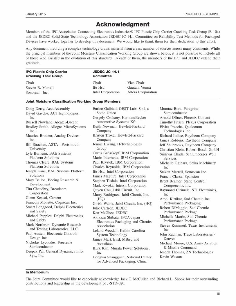
AcknowledgmentMembers of the IPC Association Connecting Electronics Industries® IPC Plastic Chip Carrier Cracking Task Group (B-10a)and the JEDEC Solid State Technology Association JEDEC JC-14.1 Committee on Reliability Test Methods for PackagedDevices have worked together to develop this document. We would like to thank them for their dedication to this effort.
Any document involving a complex technology draws material from a vast number of sources across many continents. Whilethe principal members of the Joint Moisture Classification Working Group are shown below, it is not possible to include allof those who assisted in the evolution of this standard. To each of them, the members of the IPC and JEDEC extend theirgratitude.
IPC Plastic Chip CarrierCracking Task Group
ChairSteven R. MartellSonoscan, Inc.
JEDEC JC 14.1Committee
ChairIfe HsuIntel Corporation
Vice ChairGautam VermaAltera Corporation
Joint Moisture Classification Working Group Members
Doug Derry, AccuAssemblyDavid Gaydos, ACI Technologies,
Inc.Russell Nowland, Alcatel-LucentBradley Smith, Allegro MicroSystems
Inc.Maurice Brodeur, Analog Devices
Inc.Bill Strachan, ASTA - Portsmouth
UniversityLyle Burhenn, BAE Systems
Platform SolutionsThomas Cleere, BAE Systems
Platform SolutionsJoseph Kane, BAE Systems Platform
SolutionsMary Bellon, Boeing Research &
DevelopmentTim Chaudhry, Broadcom
CorporationGlenn Koscal, CarsemFrancois Monette, Cogiscan Inc.Stuart Longgood, Delphi Electronics
and SafetyMichael Pepples, Delphi Electronics
and SafetyMark Northrup, Dynamic Research
and Testing Laboratories, LLCPaul Austen, Electronic Controls
Design Inc.Nicholas Lycoudes, Freescale
SemiconductorDeepak Pai, General Dynamics Info.
Sys., Inc.
Enrico Galbiati, GEST Labs S.r.l. aSocio Unico
Gergely Csohany, Harman/BeckerAutomotive Systems Kft.
Keith Newman, Hewlett-PackardCompany
Kristen Troxel, Hewlett-PackardCompany
Jennie Hwang, H-TechnologiesGroup
Curtis Grosskopf, IBM CorporationMario Interrante, IBM CorporationPaul Krystek, IBM CorporationCharles Reynolds, IBM CorporationIfe Hsu, Intel CorporationJames Maguire, Intel CorporationStephen Tisdale, Intel CorporationMark Kwoka, Intersil CorporationQuyen Chu, Jabil Circuit, Inc.Marty Rodriguez, Jabil Circuit, Inc.
(HQ)Girish Wable, Jabil Circuit, Inc. (HQ)Julie Carlson, JEDECKen McGhee, JEDECAkikazu Shibata, JPCA-Japan
Electronics Packaging and CircuitsAssociation
Leland Woodall, Keihin CarolinaSystem Technology
James Mark Bird, MBird andAssociates
Kurk Kan, Murata Power Solutions,Inc.
Dongkai Shangguan, National Centerfor Advanced Packaging, China
Mumtaz Bora, PeregrineSemiconductor
Arnold Offner, Phoenix ContactTimothy Pitsch, Plexus CorporationElvira Preecha, Qualcomm
Technologies Inc.Richard Iodice, Raytheon CompanyJames Robbins, Raytheon CompanyJeff Shubrooks, Raytheon CompanyChristian Klein, Robert Bosch GmbHSrinivas Chada, Schlumberger Well
ServicesMichelle Ogihara, Seika Machinery
Inc.Steven Martell, Sonoscan Inc.Francis Classe, SpansionBrent Beamer, Static Control
Components, Inc.Raymond Cirimele, STI Electronics,
Inc.Amol Kirtikar, Sud-Chemie Inc.
Performance PackagingRobert DiMaggio, Sud-Chemie
Performance PackageMichelle Martin, Sud-Chemie
Performance PackageSteven Kummerl, Texas Instruments
Inc.John Radman, Trace Laboratories -
DenverMichael Moore, U.S. Army Aviation
& Missile CommandJoseph Thomas, ZN TechnologiesKevin Weston
In Memorium
The Joint Committee would like to especially acknowledge Jack T. McCullen and Richard L. Shook for their outstandingcontributions and leadership in the development of J-STD-020.
January 2015 IPC/JEDEC J-STD-020E
iii

This Page Intentionally Left Blank
IPC/JEDEC J-STD-020E January 2015
iv
Table of Contents
1 PURPOSE.................................................................... 1
1.1 Scope .................................................................... 1
1.2 Background .......................................................... 1
1.3 Terms and Definitions.......................................... 1
1.3.1 Accelerated Equivalent Soak............................... 1
1.3.2 *Acoustic Microscope ........................................... 2
1.3.3 *Area Array Package............................................. 2
1.3.4 *Classification Temperature (Tc)........................... 2
1.3.5 Crack .................................................................... 2
1.3.6 *Damage Response................................................ 2
1.3.7 Dead-Bug (Orientation) ....................................... 2
1.3.8 Delamination ........................................................ 2
1.3.9 Downbond Area ................................................... 2
1.3.10 Floor Life ............................................................. 2
1.3.11 Full Body Hot Air Rework.................................. 2
1.3.12 Live-Bug (Orientation) ........................................ 2
1.3.13 Manufacturer’s Exposure Time (MET)............... 2
1.3.14 Moisture/Reflow Sensitivity Classification ......... 2
1.3.15 Moisture Sensitivity Level (MSL) ...................... 2
1.3.16 *Package Thickness ............................................... 2
1.3.17 *Peak Package Body Temperature (Tp) ................ 2
1.3.18 Reclassification .................................................... 2
1.3.18 *Soak...................................................................... 2
1.3.19 Wire-Bond Surface .............................................. 2
2 APPLICABLE DOCUMENTS ..................................... 3
2.1 JEDEC ................................................................ 3
2.2 IPC ...................................................................... 3
2.3 Joint Industry Standards ..................................... 3
3 APPARATUS .............................................................. 3
3.1 Temperature Humidity Chambers ....................... 3
3.2 Solder Reflow Equipment .................................. 3
3.2.1 Full Convection (Preferred)................................. 3
3.2.2 Infrared................................................................. 3
3.3 Ovens.................................................................... 4
3.4 Microscopes ........................................................ 4
3.4.1 Optical Microscope.............................................. 4
3.4.2 Acoustic Microscope ........................................... 4
3.5 Cross-Sectioning .................................................. 4
3.6 Electrical Test....................................................... 4
3.7 Weighing Apparatus (Optional)........................... 4
3.8 Beaded Thermocouple TemperatureMeasurement ........................................................ 4
4 CLASSIFICATION/RECLASSIFICATION.................... 4
4.1 Classification Temperatures (Tc) ......................... 4
4.2 Compatibility with Pb-Free AssemblyRework ................................................................. 5
4.3 Reclassification .................................................... 5
5 PROCEDURE .............................................................. 6
5.1 Sample Requirements ......................................... 6
5.1.1 Reclassification (Qualified Package withoutAdditional Reliability Testing) ............................ 6
5.1.2 Classification/Reclassification and Rework ........ 6
5.2 Initial Electrical Test............................................ 6
5.3 Initial Inspection .................................................. 6
5.4 Bake...................................................................... 6
5.5 Moisture Soak ...................................................... 6
5.6 Reflow .................................................................. 7
5.7 Final External Visual ........................................... 9
5.8 Final Electrical Test ............................................. 9
5.9 Final Acoustic Microscopy.................................. 9
6 CRITERIA ................................................................... 9
6.1 Failure Criteria after Reflow Simulation ............ 9
6.2 Criteria Requiring Further Evaluation ................ 9
6.2.1 Delamination ........................................................ 9
6.2.3 Moisture Induced Body Warpage duringBoard Assembly of Substrate BasedPackages (e.g. BGA, LGA, etc.)....................... 10
6.2.4 Bare Die with Polymer Layers.......................... 10
6.2.5 Non-IC Packages ............................................... 10
6.3 Failure Verification............................................. 10
7 MOISTURE/REFLOW SENSITIVITYCLASSIFICATION ..................................................... 10
8 OPTIONAL WEIGHT GAIN/LOSS ANALYSIS ........ 118.1 Weight Gain ....................................................... 11
8.2 Absorption Curve ............................................. 11
8.2.1 Read Points ........................................................ 11
8.2.2 Dry Weight ......................................................... 11
8.2.3 Moisture Soak .................................................... 11
8.2.4 Readouts ............................................................. 11
8.3 Desorption Curve............................................... 12
8.3.1 Read Points ........................................................ 12
8.3.2 Baking ................................................................ 12
8.3.3 Readouts............................................................. 12
9 ADDITIONS AND EXCEPTIONS .............................. 12
January 2015 IPC/JEDEC J-STD-020E
v
ANNEX A ..................................................................... 13
ANNEX B ..................................................................... 14
Figures
Figure 5-1 Classification Profile (Not to scale) ...................... 8
Tables
Table 4-1 SnPb Eutectic Process – ClassificationTemperatures (Tc) ................................................ 4
Table 4-2 Pb-Free Process – ClassificationTemperatures (Tc) ................................................ 5
Table 5-1 Moisture Sensitivity Levels................................... 7
Table 5-2 Classification Profiles ........................................... 8
Table B-1 Major Changes from Revision D toRevision E .......................................................... 14
IPC/JEDEC J-STD-020E January 2015
vi
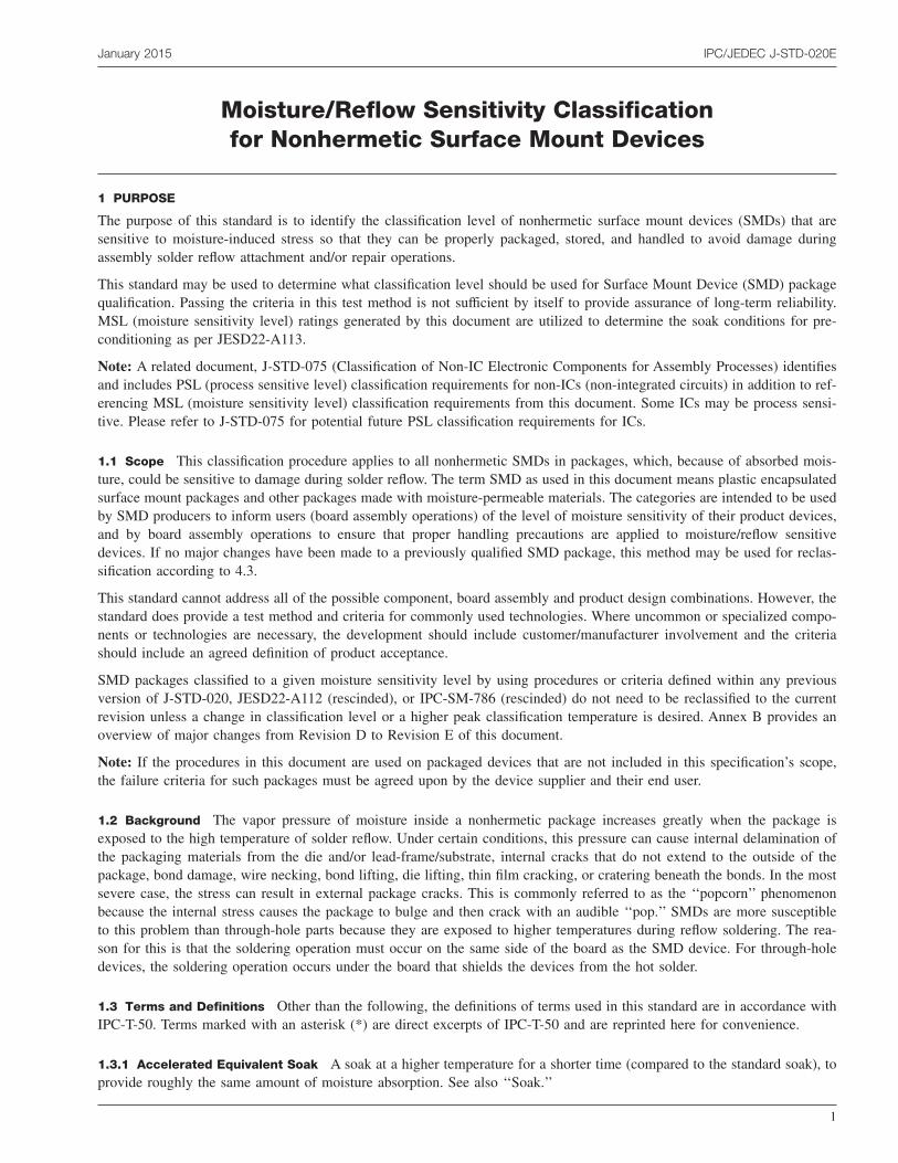
Moisture/Reflow Sensitivity Classificationfor Nonhermetic Surface Mount Devices
1 PURPOSE
The purpose of this standard is to identify the classification level of nonhermetic surface mount devices (SMDs) that aresensitive to moisture-induced stress so that they can be properly packaged, stored, and handled to avoid damage duringassembly solder reflow attachment and/or repair operations.
This standard may be used to determine what classification level should be used for Surface Mount Device (SMD) packagequalification. Passing the criteria in this test method is not sufficient by itself to provide assurance of long-term reliability.MSL (moisture sensitivity level) ratings generated by this document are utilized to determine the soak conditions for pre-conditioning as per JESD22-A113.
Note: A related document, J-STD-075 (Classification of Non-IC Electronic Components for Assembly Processes) identifiesand includes PSL (process sensitive level) classification requirements for non-ICs (non-integrated circuits) in addition to ref-erencing MSL (moisture sensitivity level) classification requirements from this document. Some ICs may be process sensi-tive. Please refer to J-STD-075 for potential future PSL classification requirements for ICs.
1.1 Scope This classification procedure applies to all nonhermetic SMDs in packages, which, because of absorbed mois-ture, could be sensitive to damage during solder reflow. The term SMD as used in this document means plastic encapsulatedsurface mount packages and other packages made with moisture-permeable materials. The categories are intended to be usedby SMD producers to inform users (board assembly operations) of the level of moisture sensitivity of their product devices,and by board assembly operations to ensure that proper handling precautions are applied to moisture/reflow sensitivedevices. If no major changes have been made to a previously qualified SMD package, this method may be used for reclas-sification according to 4.3.
This standard cannot address all of the possible component, board assembly and product design combinations. However, thestandard does provide a test method and criteria for commonly used technologies. Where uncommon or specialized compo-nents or technologies are necessary, the development should include customer/manufacturer involvement and the criteriashould include an agreed definition of product acceptance.
SMD packages classified to a given moisture sensitivity level by using procedures or criteria defined within any previousversion of J-STD-020, JESD22-A112 (rescinded), or IPC-SM-786 (rescinded) do not need to be reclassified to the currentrevision unless a change in classification level or a higher peak classification temperature is desired. Annex B provides anoverview of major changes from Revision D to Revision E of this document.
Note: If the procedures in this document are used on packaged devices that are not included in this specification’s scope,the failure criteria for such packages must be agreed upon by the device supplier and their end user.
1.2 Background The vapor pressure of moisture inside a nonhermetic package increases greatly when the package isexposed to the high temperature of solder reflow. Under certain conditions, this pressure can cause internal delamination ofthe packaging materials from the die and/or lead-frame/substrate, internal cracks that do not extend to the outside of thepackage, bond damage, wire necking, bond lifting, die lifting, thin film cracking, or cratering beneath the bonds. In the mostsevere case, the stress can result in external package cracks. This is commonly referred to as the ‘‘popcorn’’ phenomenonbecause the internal stress causes the package to bulge and then crack with an audible ‘‘pop.’’ SMDs are more susceptibleto this problem than through-hole parts because they are exposed to higher temperatures during reflow soldering. The rea-son for this is that the soldering operation must occur on the same side of the board as the SMD device. For through-holedevices, the soldering operation occurs under the board that shields the devices from the hot solder.
1.3 Terms and Definitions Other than the following, the definitions of terms used in this standard are in accordance withIPC-T-50. Terms marked with an asterisk (*) are direct excerpts of IPC-T-50 and are reprinted here for convenience.
1.3.1 Accelerated Equivalent Soak A soak at a higher temperature for a shorter time (compared to the standard soak), toprovide roughly the same amount of moisture absorption. See also ‘‘Soak.’’
January 2015 IPC/JEDEC J-STD-020E
1
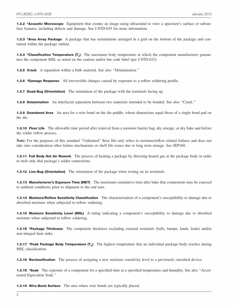
1.3.2 *Acoustic Microscope Equipment that creates an image using ultrasound to view a specimen’s surface or subsur-face features, including defects and damage. See J-STD-035 for more information.
1.3.3 *Area Array Package A package that has terminations arranged in a grid on the bottom of the package and con-tained within the package outline.
1.3.4 *Classification Temperature (Tc) The maximum body temperature at which the component manufacturer guaran-tees the component MSL as noted on the caution and/or bar code label (per J-STD-033).
1.3.5 Crack A separation within a bulk material. See also ‘‘Delamination.’’
1.3.6 *Damage Response All irreversible changes caused by exposure to a reflow soldering profile.
1.3.7 Dead-Bug (Orientation) The orientation of the package with the terminals facing up.
1.3.8 Delamination An interfacial separation between two materials intended to be bonded. See also ‘‘Crack.’’
1.3.9 Downbond Area An area for a wire bond on the die paddle, whose dimensions equal those of a single bond pad onthe die.
1.3.10 Floor Life The allowable time period after removal from a moisture barrier bag, dry storage, or dry bake and beforethe solder reflow process.
Note: For the purposes of this standard ‘‘Unlimited’’ floor life only refers to moisture/reflow related failures and does nottake into consideration other failure mechanisms or shelf life issues due to long term storage. See JEP160.
1.3.11 Full Body Hot Air Rework The process of heating a package by directing heated gas at the package body in orderto melt only that package’s solder connections.
1.3.12 Live-Bug (Orientation) The orientation of the package when resting on its terminals.
1.3.13 Manufacturer’s Exposure Time (MET) The maximum cumulative time after bake that components may be exposedto ambient conditions prior to shipment to the end user.
1.3.14 Moisture/Reflow Sensitivity Classification The characterization of a component’s susceptibility to damage due toabsorbed moisture when subjected to reflow soldering.
1.3.15 Moisture Sensitivity Level (MSL) A rating indicating a component’s susceptibility to damage due to absorbedmoisture when subjected to reflow soldering.
1.3.16 *Package Thickness The component thickness excluding external terminals (balls, bumps, lands, leads) and/ornon-integral heat sinks.
1.3.17 *Peak Package Body Temperature (Tp) The highest temperature that an individual package body reaches duringMSL classification.
1.3.18 Reclassification The process of assigning a new moisture sensitivity level to a previously classified device.
1.3.18 *Soak The exposure of a component for a specified time at a specified temperature and humidity. See also ‘‘Accel-erated Equivalent Soak.’’
1.3.19 Wire-Bond Surface The area where wire bonds are typically placed.
IPC/JEDEC J-STD-020E January 2015
2
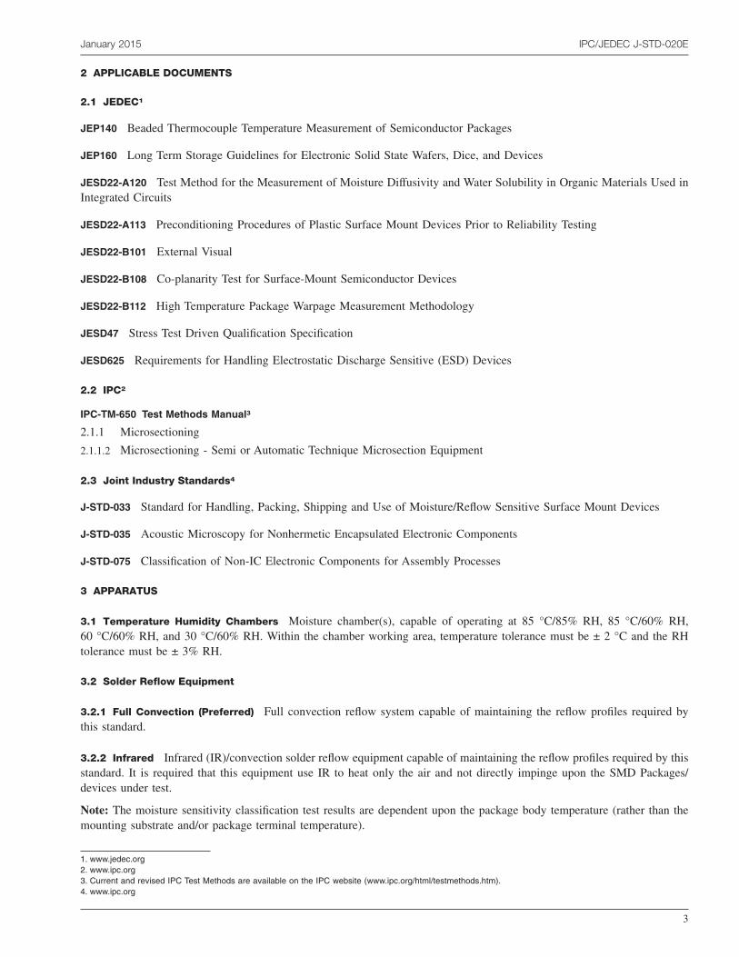
2 APPLICABLE DOCUMENTS
2.1 JEDEC1
JEP140 Beaded Thermocouple Temperature Measurement of Semiconductor Packages
JEP160 Long Term Storage Guidelines for Electronic Solid State Wafers, Dice, and Devices
JESD22-A120 Test Method for the Measurement of Moisture Diffusivity and Water Solubility in Organic Materials Used inIntegrated Circuits
JESD22-A113 Preconditioning Procedures of Plastic Surface Mount Devices Prior to Reliability Testing
JESD22-B101 External Visual
JESD22-B108 Co-planarity Test for Surface-Mount Semiconductor Devices
JESD22-B112 High Temperature Package Warpage Measurement Methodology
JESD47 Stress Test Driven Qualification Specification
JESD625 Requirements for Handling Electrostatic Discharge Sensitive (ESD) Devices
2.2 IPC2
IPC-TM-650 Test Methods Manual3
2.1.1 Microsectioning
2.1.1.2 Microsectioning - Semi or Automatic Technique Microsection Equipment
2.3 Joint Industry Standards4
J-STD-033 Standard for Handling, Packing, Shipping and Use of Moisture/Reflow Sensitive Surface Mount Devices
J-STD-035 Acoustic Microscopy for Nonhermetic Encapsulated Electronic Components
J-STD-075 Classification of Non-IC Electronic Components for Assembly Processes
3 APPARATUS
3.1 Temperature Humidity Chambers Moisture chamber(s), capable of operating at 85 °C/85% RH, 85 °C/60% RH,60 °C/60% RH, and 30 °C/60% RH. Within the chamber working area, temperature tolerance must be ± 2 °C and the RHtolerance must be ± 3% RH.
3.2 Solder Reflow Equipment
3.2.1 Full Convection (Preferred) Full convection reflow system capable of maintaining the reflow profiles required bythis standard.
3.2.2 Infrared Infrared (IR)/convection solder reflow equipment capable of maintaining the reflow profiles required by thisstandard. It is required that this equipment use IR to heat only the air and not directly impinge upon the SMD Packages/devices under test.
Note: The moisture sensitivity classification test results are dependent upon the package body temperature (rather than themounting substrate and/or package terminal temperature).
1. www.jedec.org2. www.ipc.org3. Current and revised IPC Test Methods are available on the IPC website (www.ipc.org/html/testmethods.htm).4. www.ipc.org
January 2015 IPC/JEDEC J-STD-020E
3
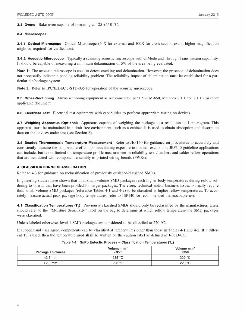
3.3 Ovens Bake oven capable of operating at 125 +5/-0 °C.
3.4 Microscopes
3.4.1 Optical Microscope Optical Microscope (40X for external and 100X for cross-section exam, higher magnificationmight be required for verification).
3.4.2 Acoustic Microscope Typically a scanning acoustic microscope with C-Mode and Through Transmission capability.It should be capable of measuring a minimum delamination of 5% of the area being evaluated.
Note 1: The acoustic microscope is used to detect cracking and delamination. However, the presence of delamination doesnot necessarily indicate a pending reliability problem. The reliability impact of delamination must be established for a par-ticular die/package system.
Note 2: Refer to IPC/JEDEC J-STD-035 for operation of the acoustic microscope.
3.5 Cross-Sectioning Micro-sectioning equipment as recommended per IPC-TM-650, Methods 2.1.1 and 2.1.1.2 or otherapplicable document.
3.6 Electrical Test Electrical test equipment with capabilities to perform appropriate testing on devices.
3.7 Weighing Apparatus (Optional) Apparatus capable of weighing the package to a resolution of 1 microgram. Thisapparatus must be maintained in a draft-free environment, such as a cabinet. It is used to obtain absorption and desorptiondata on the devices under test (see Section 8).
3.8 Beaded Thermocouple Temperature Measurement Refer to JEP140 for guidance on procedures to accurately andconsistently measure the temperature of components during exposure to thermal excursions. JEP140 guideline applicationscan include, but is not limited to, temperature profile measurement in reliability test chambers and solder reflow operationsthat are associated with component assembly to printed wiring boards (PWBs).
4 CLASSIFICATION/RECLASSIFICATION
Refer to 4.3 for guidance on reclassification of previously qualified/classified SMDs.
Engineering studies have shown that thin, small volume SMD packages reach higher body temperatures during reflow sol-dering to boards that have been profiled for larger packages. Therefore, technical and/or business issues normally requirethin, small volume SMD packages (reference Tables 4-1 and 4-2) to be classified at higher reflow temperatures. To accu-rately measure actual peak package body temperatures, refer to JEP140 for recommended thermocouple use.
4.1 Classification Temperatures (Tc) Previously classified SMDs should only be reclassified by the manufacturer. Usersshould refer to the ‘‘Moisture Sensitivity’’ label on the bag to determine at which reflow temperature the SMD packageswere classified.
Unless labeled otherwise, level 1 SMD packages are considered to be classified at 220 °C.
If supplier and user agree, components can be classified at temperatures other than those in Tables 4-1 and 4-2. If a differ-ent Tc is used, then the temperature used shall be written on the caution label as defined in J-STD-033.
Table 4-1 SnPb Eutectic Process – Classification Temperatures (Tc)
Package ThicknessVolume mm3
<350Volume mm3
≥350
<2.5 mm 235 °C 220 °C
≥2.5 mm 220 °C 220 °C
IPC/JEDEC J-STD-020E January 2015
4
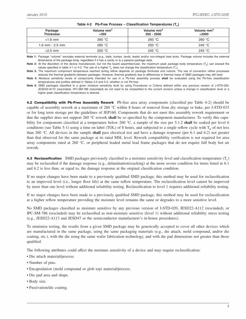
4.2 Compatibility with Pb-Free Assembly Rework Pb-free area array components (classified per Table 4-2) should becapable of assembly rework at a maximum of 260 °C within 8 hours of removal from dry storage or bake, per J-STD-033or for long term storage per the guidelines of JEP160. Components that do not meet this assembly rework requirement orthat the supplier does not support 260 °C rework shall be so specified by the component manufacturer. To verify this capa-bility for components classified at a temperature below 260 °C, a sample of the size per 5.1.2 shall be soaked per level 6conditions (see Table 5-1) using a time on label (TOL) of 8 hours, and subjected to a single reflow cycle with Tp of not lessthan 260 °C. All devices in the sample shall pass electrical test and have a damage response (per 6.1 and 6.2) not greaterthan that observed for the same package at its rated MSL level. Rework compatibility verification is not required for areaarray components rated at 260 °C. or peripheral leaded metal lead frame packages that do not require full body hot airrework.
4.3 Reclassification SMD packages previously classified to a moisture sensitivity level and classification temperature (Tc)may be reclassified if the damage response (e.g., delamination/cracking) at the more severe condition for items listed in 6.1and 6.2 is less than, or equal to, the damage response at the original classification condition.
If no major changes have been made to a previously qualified SMD package, this method may be used for reclassificationto an improved level (i.e., longer floor life) at the same reflow temperature. The reclassification level cannot be improvedby more than one level without additional reliability testing. Reclassification to level 1 requires additional reliability testing.
If no major changes have been made to a previously qualified SMD package, this method may be used for reclassificationat a higher reflow temperature providing the moisture level remains the same or degrades to a more sensitive level.
No SMD packages classified as moisture sensitive by any previous version of J-STD-020, JESD22-A112 (rescinded), orIPC-SM-786 (rescinded) may be reclassified as non-moisture sensitive (level 1) without additional reliability stress testing(e.g., JESD22-A113 and JESD47 or the semiconductor manufacturer’s in-house procedures).
To minimize testing, the results from a given SMD package may be generically accepted to cover all other devices whichare manufactured in the same package, using the same packaging materials (e.g., die attach, mold compound, and/or diecoating, etc.), with the die using the same wafer fabrication technology, and with die pad dimensions not greater than thosequalified.
The following attributes could affect the moisture sensitivity of a device and may require reclassification:
• Die attach material/process.
• Number of pins.
• Encapsulation (mold compound or glob top) material/process.
• Die pad area and shape.
• Body size.
• Passivation/die coating.
Table 4-2 Pb-Free Process – Classification Temperatures (Tc)
PackageThickness
Volume mm3
<350Volume mm3
350 - 2000Volume mm3
>2000
<1.6 mm 260 °C 260 °C 260 °C
1.6 mm - 2.5 mm 260 °C 250 °C 245 °C
>2.5 mm 250 °C 245 °C 245 °C
Note 1: Package ‘‘volume’’ excludes external terminals (e.g., balls, bumps, lands, leads) and/or non-integral heat sinks. Package volume includes the externaldimensions of the package body, regardless if it has a cavity or is a passive package style.
Note 2: At the discretion of the device manufacturer, but not the board assembler/user, the maximum peak package body temperature (Tp) can exceed thevalues specified in table 4-1 or 4-2. The use of a higher Tp does not change the classification temperature (Tc).
Note 3: The maximum component temperature reached during reflow depends on package thickness and volume. The use of convection reflow processesreduces the thermal gradients between packages. However, thermal gradients due to differences in thermal mass of SMD packages may still exist.
Note 4: Moisture sensitivity levels of components intended for use in a Pb-free assembly process shall be evaluated using the Pb-free classificationtemperatures and profiles defined in Tables 4-2 and 5-2, whether or not Pb-free.
Note 5: SMD packages classified to a given moisture sensitivity level by using Procedures or Criteria defined within any previous version of J-STD-020,JESD22-A112 (rescinded), IPC-SM-786 (rescinded) do not need to be reclassified to the current revision unless a change in classification level or ahigher peak classification temperature is desired.
January 2015 IPC/JEDEC J-STD-020E
5
• Leadframe, substrate, and/or heat spreader design/material/finish.
• Die size/thickness.
• Wafer fabrication technology/process.
• Interconnect.
• Lead lock taping size/location as well as material.
5 PROCEDURE
The recommended procedure is to start testing at the lowest moisture sensitivity level the evaluation package is reasonablyexpected to pass (based on knowledge of other similar evaluation packages).
In the case of equipment malfunction, operator error, or electrical power loss, engineering judgment shall be used to ensurethat the minimum intent/requirements of this specification are met.
5.1 Sample Requirements
5.1.1 Reclassification (Qualified Package without Additional Reliability Testing) For a qualified SMD package beingreclassified without additional reliability testing, select a minimum sample of 22 units for each moisture sensitivity level tobe tested. A minimum of two nonconsecutive assembly lots must be included in the sample with each lot having approxi-mately the same representation. Sample units shall have completed all manufacturing processing required prior to shipment.Sample groups may be run concurrently on one or more moisture sensitivity levels.
5.1.2 Classification/Reclassification and Rework Select a minimum sample of 11 units for each moisture sensitivitylevel to be tested. A minimum of two nonconsecutive assembly lots must be included in the sample with each lot havingapproximately the same representation. Sample units shall have completed all manufacturing processes required prior toshipment. Sample groups may be run concurrently on one or more moisture sensitivity levels. Testing must be continueduntil a passing level is found.
SMD packages should not be reclassified by the user unless approved by the supplier.
5.2 Initial Electrical Test Test appropriate electrical parameters (e.g., data sheet values, in house specifications, etc.).Replace any components, while maintaining the sample requirements of 5.1.2, which fail to meet tested parameters.
5.3 Initial Inspection Perform an external visual (at 40X) and acoustic microscope examination on all components toestablish a baseline for the cracking/delamination criteria in 6.2.1.
Note: This standard does not consider or establish any accept/reject criteria for delamination at initial/time zero inspection.
5.4 Bake Bake the sample for 24 hours minimum at 125 +5/-0 °C. This step is intended to remove moisture from thepackage so that it will be ‘‘dry.’’
Note 1: This time/temperature may be modified if desorption data on the particular device under test shows that a differentcondition is required to obtain a ‘‘dry’’ package when starting in the wet condition for 85 °C/85% RH (see 8.3).
Note 2: If a bake test is interrupted for greater than 15 minutes; then the total time of the interruption should be excludedfrom the bake time. The interruption time should be accounted and no greater than 1 hour, then re-incorporated to ensureminimum of 24 hours. For instance, if the interruption was 45 minute, then the total bake test time would be 24 hours and45 minutes. If greater than 1 hour the bake should be restarted for a full 24 hours.
5.5 Moisture Soak Place devices in a clean, dry, shallow container so that the package bodies do not touch or overlapeach other. Submit each sample to the appropriate soak requirements shown in Table 5-1. At all times parts should behandled using proper ESD procedures in accordance with JESD625.
IPC/JEDEC J-STD-020E January 2015
6
5.6 Reflow Not sooner than 15 minutes and not longer than 4 hours after removal from the temperature/humidity cham-ber, subject the sample to 3 cycles of the appropriate reflow conditions as defined in Table 5-2 and Figure 5-1. If the tim-ing between removal from the temperature/humidity chamber and initial reflow cannot be met, then the parts must berebaked and resoaked according to 5.4 and 5.5. The time between reflows shall be 5 minutes minimum and 60 minutesmaximum.
Note 1: All temperatures refer to the center of the package, measured on the package body surface that is facing up duringassembly reflow (e.g., live-bug orientation).
If parts are reflowed in other than the normal live bug assembly reflow orientation, (i.e., dead-bug orientation), Tp shall bewithin ± 2 °C of the live bug Tp and still meet the Tc requirements, otherwise the profile shall be adjusted to achieve thelatter.
To accurately measure actual peak package body temperatures refer to JEP140 for recommended thermocouple use.
Note 2: The oven should be loaded with the same configuration or verified equivalent thermal load when running parts orbeing profiled.
Table 5-1 Moisture Sensitivity Levels
LEVEL
FLOOR LIFE4
SOAK REQUIREMENTS3
STANDARD
ACCELERATED EQUIVALENT1
eV0.40-0.48
eV0.30-0.39
CONDITIONTIME CONDITION TIME (hours) CONDITION TIME (hours) TIME (hours)
1 Unlimited ≤30 °C/85%RH
168+5/-0
85 °C/85%RH NA NA NA
2 1 year ≤30 °C/60%RH
168+5/-0
85 °C/60%RH NA NA NA
2a 4 weeks ≤30 °C/60%RH
6962
+5/-030 °C/60%
RH120
+1/-0168
+1/-060 °C/60%
RH
3 168 hours ≤30 °C/60%RH
1922
+5/-030 °C/60%
RH40
+1/-052
+1/-060 °C/60%
RH
4 72 hours ≤30 °C/60%RH
962
+2/-030 °C/60%
RH20
+0.5/-024
+0.5/-060 °C/60%
RH
5 48 hours ≤30 °C/60%RH
722
+2/-030 °C/60%
RH15
+0.5/-020
+0.5/-060 °C/60%
RH
5a 24 hours ≤30 °C/60%RH
482
+2/-030 °C/60%
RH10
+0.5/-013
+0.5/-060 °C/60%
RH
6 Time on Label(TOL)
≤30 °C/60%RH TOL 30 °C/60%
RH NA NA NA
Note 1: CAUTION - To use the ‘‘accelerated equivalent’’ soak conditions, correlation of damage response (including electrical, after soak and reflow), should beestablished with the ‘‘standard’’ soak conditions. Alternatively, if the known activation energy (eV) for moisture diffusion of the package materials is inthe range of 0.40 - 0.48 eV or 0.30 - 0.39 eV, the ‘‘accelerated equivalent’’ may be used. Accelerated soak times may vary due to material properties(e.g., mold compound, encapsulant, etc.). JEDEC document JESD22-A120 provides a method for determining the eV.
Note 2: The standard soak time includes a default value of 24 hours for semiconductor manufacturer’s exposure time (MET) between bake and bag andincludes the maximum time allowed out of the bag at the distributor’s facility.
If the actual MET is less than 24 hours, the soak time may be reduced. For soak conditions of 30 °C/60% RH, the soak time is reduced by 1 hour foreach hour the MET is less than 24 hours. For soak conditions of 60 °C/60% RH, the soak time is reduced by 1 hour for each 5 hours the MET is lessthan 24 hours.
If the actual MET is greater than 24 hours the soak time must be increased. If soak conditions are 30 °C/60% RH, the soak time is increased 1 hourfor each hour that the actual MET exceeds 24 hours. If soak conditions are 60 °C/60% RH, the soak time is increased 1 hour for each 5 hours that theactual MET exceeds 24 hours.
Note 3: Supplier may extend the soak times at their own risk.Note 4: ‘‘Floor Life’’ only relates to moisture/reflow related failures and does not take into consideration other failure mechanisms or ‘‘shelf life’’ issues due to
long term storage.Note 5: Table 5-1 accelerated soak requirements may not apply to mold compounds that do not contain fillers.
January 2015 IPC/JEDEC J-STD-020E
7
Table 5-2 Classification Profiles
Profile Feature Sn-Pb Eutectic Assembly Pb-Free Assembly
Preheat/SoakTemperature Min (Tsmin)Temperature Max (Tsmax)Time (ts) from (Tsmin to Tsmax)
100 °C150 °C
60-120 seconds
150 °C200 °C
60-120 seconds
Ramp-up rate (TL to Tp) 3 °C/second max. 3 °C/second max.
Liquidous temperature (TL)Time (tL) maintained above TL
183 °C60-150 seconds
217 °C60-150 seconds
Peak package body temperature (Tp)
For users Tp must not exceed theClassification temp in Table 4-1.
For suppliers Tp must equal or exceedthe Classification temp in Table 4-1.
For users Tp must not exceed theClassification temp in Table 4-2.
For suppliers Tp must equal or exceedthe Classification temp in Table 4-2.
Time (tp)* within 5 °C of the specified classi-fication temperature (Tc), see Figure 5-1. 20* seconds 30* seconds
Ramp-down rate (Tp to TL) 6 °C/second max. 6 °C/second max.
Time 25 °C to peak temperature 6 minutes max. 8 minutes max.
* Tolerance for peak profile temperature (Tp) is defined as a supplier minimum and a user maximum.
Note 1: All temperatures refer to the center of the package, measured on the package body surface that is facing up during assembly reflow (e.g., live-bug). Ifparts are reflowed in other than the normal live bug assembly reflow orientation (i.e., dead-bug), Tp shall be within ± 2 °C of the live bug Tp and stillmeet the Tc requirements, otherwise, the profile shall be adjusted to achieve the latter. To accurately measure actual peak package bodytemperatures, refer to JEP140 for recommended thermocouple use.
Note 2: Reflow profiles in this document are for classification/preconditioning and are not meant to specify board assembly profiles. Actual board assemblyprofiles should be developed based on specific process needs and board designs and should not exceed the parameters in this table.
For example, if Tc is 260 °C and time Tp is 30 seconds, this means the following for the supplier and the user:
b For a supplier: The peak temperature must be at least 260 °C. The time above 255 °C must be at least 30 seconds.
b For a user: The peak temperature must not exceed 260 °C. The time above 255 °C must not exceed 30 seconds.Note 3: All components in the test load shall meet the classification profile requirements.Note 4: SMD packages classified to a given moisture sensitivity level by using Procedures or Criteria defined within any previous version of J-STD-020,
JESD22-A112 (rescinded), IPC-SM-786 (rescinded) do not need to be reclassified to the current revision unless a change in classification level or ahigher peak classification temperature is desired.
IPC-020e-5-1
Figure 5-1 Classification Profile (Not to scale)
Tc -5°C
t
Max. Ramp Up Rate = 3°C/sMax. Ramp Down Rate = 6°C/s
Preheat AreaTsmax
Tsmin
ts
Tp
TL
Te
mp
era
ture
Time
25Time 25°C to Peak
Supplier Tp > Tc-
Supplier tp
Tc
User Tp < Tc -
User tp
Tc -5°C
tp
IPC/JEDEC J-STD-020E January 2015
8
5.7 Final External Visual Examine the devices using an optical microscope (at 40X) to look for external cracks.
5.8 Final Electrical Test Perform appropriate electrical testing on all devices, (e.g., data sheet values, in-house specifica-tions, etc.).
Note: Considerations should be taken for lead oxidation or other mechanisms due to baking that may affect the electricaltesting of the devices.
5.9 Final Acoustic Microscopy Perform acoustic microscope analysis on all devices.
6 CRITERIA
6.1 Failure Criteria after Reflow Simulation If one or more devices in the test sample denoted in 5.1 fail, the packageshall be considered to have failed the tested level.
A device is considered a failure if it exhibits any of the following:
a. External crack visible using 40X optical microscope. It is highly desired to use 100X optical magnification or low vacuumscanning electron microscopy (SEM) to better observe any cracks that could be precursors to problems during the stressof operational life.
b. Electrical test failure.
c. Internal crack that intersects a bond wire, ball bond, or wedge bond.
d. Internal crack extending from any lead finger to any other internal feature (lead finger, chip, die attach paddle).
e. Internal crack extending more than 2/3 the distance from any internal feature to the outside of the package.
f. Changes in package body flatness caused by warpage, swelling, or bulging not visible to the naked eye per JESD22-B101.If parts still meet co-planarity and standoff dimensions as measured at room temperature per JESD22-B108, they shallbe considered passing.
If the components pass the requirements of 6.1, and there is no evidence of cracks observed by acoustic microscopy or othermeans, the component is considered to pass that level of moisture sensitivity. If internal mold compound cracks are indi-cated by acoustic microscopy, they must be considered a failure or verified that it has not failed the criteria above usingpolished cross sections through the identified site.
Note 1: For packages known to be sensitive to vertical cracks, it is recommended that polished cross sections be used toconfirm the nonexistence of near vertical cracks within the mold compound or encapsulant.
Note 2: Failing SMD packages must be evaluated to a higher numeric level of moisture sensitivity (i.e., more susceptible)using a new set of samples.
6.2 Criteria Requiring Further Evaluation Delamination is not necessarily a cause for rejection. To evaluate the impact ofdelamination on device reliability, the semiconductor manufacturer may either meet the delamination requirements shown in6.2.1 or perform reliability assessment using JESD22-A113 and JESD47 or the semiconductor manufacturer’s in-house pro-cedures. The reliability assessment may consist of stress testing, historical generic data analysis, etc. Annex A shows thelogic flow diagram for the implementation of these criteria.
If the SMD Packages pass electrical tests and there is delamination on the back side of the die paddle, heat spreader, or dieback side (lead on chip only), but there is no evidence of cracking or other delamination and they still meet specifieddimensional criteria, the SMD Packages are considered to pass that level of moisture sensitivity.
6.2.1 Delamination The following delamination change criteria for the specific package type are measured from pre-moisture soak to post reflow. A delamination change is the difference between pre- and post-reflow delamination. The per-cent (%) delamination or delamination change is calculated in relation to the total area being evaluated.
6.2.1.1 Metal Lead-Frame Packages:
a. No delamination on the active side of the die.
b. No delamination on any wire bonding surface including the downbond area or the lead-frame of lead on chip (LOC)devices.
January 2015 IPC/JEDEC J-STD-020E
9
c. No delamination change >10% along any polymeric film bridging any metallic features that is designed to be isolated(verifiable by through transmission acoustic microscopy).
d. No delamination/cracking >50% of the die attach area:1. In packages with exposed die pad used for thermal conductivity or2. For devices that require electrical contact to the backside of the die
e. No surface-breaking feature delaminated over its entire length. A surface-breaking feature includes lead fingers, tie bars,heat spreader alignment features, heat slugs, etc.
6.2.1.2 Substrate Based Packages (e.g., BGA, LGA, etc.):
a. No delamination on the active side of the die.
b. No delamination on any wire bonding surface of the laminate.
c. No delamination change >10% along the polymer potting or molding compound/laminate interface for cavity and over-molded packages.
d. No delamination change >10% along the solder mask/laminate resin interface.
e. No delamination change >10% within the laminate.
f. No delamination/cracking change >10% through the die attach region.
g. No delamination/cracking between underfill resin and chip or underfill resin and substrate/solder mask.
h. No surface-breaking feature delaminated over its entire length. A surface-breaking feature includes lead fingers, laminate,laminate metallization, PTH, heat slugs, etc.
Note 1: On substrate based packages, the C-mode acoustic image is not easy to interpret. Through Transmission AcousticImaging is recommended to supplement and verify the C-mode images because it is easier to interpret and more reliable. Ifit is necessary to verify results or determine at what level in the package the cracking/delamination is occurring, cross-sectional analysis should be used.
6.2.3 Moisture Induced Body Warpage during Board Assembly of Substrate Based Packages (e.g. BGA, LGA, etc.)
Moisture Induced warpage could result in solder bridging or open connections during board assembly solder attachmentoperations. It is known that ingressed moisture can either increase or decrease the total package body warpage dependingon the specific design of the component. Total package body warpage can be a function of the moisture content and can beaffected by the ramp rates and dwells used to measure the total warpage effect at elevated temperatures. Package body war-page measured per JESD22-B112 should be characterized during package development and any time there are changes ofthe type denoted in section 4.3. Ability to attach components that exhibit warpage can be verified by using board assembly.
6.2.4 Bare Die with Polymer Layers Currently J-STD-020 does not provide failure criteria for the package style of baredie with polymer layers. Any party choosing to use the procedures within this standard to determine MSL rating for thistype of package style is responsible for defining the appropriate failure criteria to ensure the long term reliability of thedevice.
6.2.5 Non-IC Packages Currently J-STD-020 does not provide failure criteria for non-IC package styles. Any partychoosing to use the procedure within this standard to determine the MSL rating for a non-IC package is responsible fordefining the appropriate failure criteria to ensure the long term reliability of the device.
6.3 Failure Verification All failures should be analyzed to confirm that the failure mechanism is associated with moisturesensitivity. If there are no reflow moisture-sensitive-induced failures in the level selected, the component meets the testedlevel of moisture sensitivity.
If the acoustic microscope scans show failure to any of the criteria listed in 6.2.1, the SMD Packages shall be tested to ahigher numeric level of moisture sensitivity or subjected to a reliability assessment using JESD22-A113 and JESD47 or thesemiconductor manufacturer’s in-house procedures.
7 MOISTURE/REFLOW SENSITIVITY CLASSIFICATION
If a device passes level 1, it is classified as not moisture sensitive and does not require dry pack. Other factors beyond MSLmay need to be considered, such as those included in JEP160, for long term storage.
IPC/JEDEC J-STD-020E January 2015
10
If a device fails level 1 but passes a higher numerical level, it is classified as moisture sensitive and must be dry packed inaccordance with J-STD-033, and, if required for long term storage, per the guidelines of JEP160 for long term storage.
If a device will pass only level 6, it is classified as extremely moisture sensitive and dry pack will not provide adequateprotection. If this product is shipped, the customer must be advised of its classification. The supplier must also include awarning label with the device indicating that it either is socket mounted, or baked dry within TOL (Time on Label) beforereflow soldering. The minimum bake time and temperature should be determined from desorption studies of the device undertest (see 8.3).
8 OPTIONAL WEIGHT GAIN/LOSS ANALYSIS
8.1 Weight Gain Weight gain analysis (absorption) can be very valuable in determining estimated floor life (the time fromremoval of a device from dry pack until it absorbs sufficient moisture to be at risk during reflow soldering). Weight lossanalysis (desorption) is valuable in determining the bake time required to remove excess moisture from a device so that itwill no longer be at risk during reflow soldering. Weight gain/loss is calculated using an average for the entire sample. It isrecommended that ten (10) components be used in the sample. Dependent on weight, components may be weighed indi-vidually or in group(s).
Final weight gain = (wet weight - dry weight)/dry weight.Final weight loss = (wet weight - dry weight)/wet weight.Interim weight gain = (present weight - dry weight)/dry weight.Interim weight loss = (wet weight - present weight)/wet weight.
‘‘Wet’’ is relative and means the package is exposed to moisture under specific temperature and humidity conditions.
‘‘Dry’’ is specific and means no additional moisture can be removed from the package at 125 °C as per 8.2.2.
8.2 Absorption Curve
8.2.1 Read Points The X-axis (time) read points should be selected for plotting the absorption curve. For the early read-ings, points should be relatively short (24 hours or less) because the curve will have a steep initial slope. Later readings maybe spread out further (10 days or more) as the curve becomes asymptotic. The Y-axis (weight gain) should start with ‘‘0’’and increase to the saturated weight gain. Most devices will reach saturation between 0.3% and 0.4% when stored at 85°C/85% RH. Use the formula in 8.1. Devices shall be kept at room ambient between removal from the oven or chamber andweighing and subsequent reinsertion into the oven or chamber.
8.2.2 Dry Weight The dry weight of the sample shall be determined first by baking the sample for 24 hours at 125 +5/-0°C; continued baking and weighing of the sample every 12 hours is recommended until no further weight loss is observedto ensure that the devices are dry. The dry weight is determined when no further weight loss is observed after two consecu-tive measurements with a minimum baking interval of 12 hours. Characterization outside recommended 12 hour intervalswill possibly require more data points to determine weight loss stabilization and prolong this process.
Within 1 hour after removal from the oven, weigh the devices using the optional equipment in 3.7 and determine an aver-age dry weight per 8.1. For small SMDs (less than 1.5 mm total height), devices should be weighed within 30 minutes afterremoval from oven.
Note: If bake is interrupted for greater than 15 minutes the total time of the interruption should be added to the bake time.The interruption time should be accounted and no greater than 1 hour, then re-incorporated to ensure minimum of 24 hours.For instance, if the interruption was 45 minute, then the total bake test time would be 24 hours and 45 minutes. If greaterthan 1 hour the bake should be restarted for a full 24 hours.
8.2.3 Moisture Soak Within 1 hour after weighing, place the devices in a clean, dry, shallow container so that the pack-age bodies do not touch each other. Place the devices in the desired temperature/humidity condition for the desired lengthof time.
8.2.4 Readouts Upon removal of the devices from the temperature/humidity chamber, allow devices to cool for at least15 minutes. Within 1 hour after removal from the chamber, weigh the devices. For small SMDs (less than 1.5 mm totalheight), devices should be weighed within 30 minutes after removal from the chamber. After the devices are weighed, fol-low the procedure in 8.2.3 for placing the devices back in the temperature/humidity chamber. No more than 2 hours totaltime should elapse between removal of devices from the temperature/humidity chamber and their return to the chamber.
January 2015 IPC/JEDEC J-STD-020E
11
Continue alternating between 8.2.3 and 8.2.4 until the devices reach saturation as indicated by no additional increase inmoisture absorption or until soaked to the maximum time of interest.
8.3 Desorption Curve A desorption curve can be plotted using devices that have reached saturation as determined in 8.2.
8.3.1 Read Points The suggested read points on the X-axis are 12 hour intervals. The Y-axis should run from ‘‘0’’ weightgain to the saturated value as determined in 8.2.
8.3.2 Baking Within 1 hour (but not sooner than 15 minutes) after removal of the saturated devices from the temperature/humidity chamber, place the devices in a clean, dry, shallow container so that the package bodies do not touch each other.Place the devices in the bake oven at the desired temperature for the desired time.
8.3.3 Readouts At the desired read point; remove the devices from the bake oven. Within 1 hour after removal of thedevices from the bake oven, remove the devices from the container and determine their average weight using the optionalequipment in 3.7 and formula in 8.1.
Within 1 hour after weighing the devices, place them in a clean, dry, shallow container so that the package bodies do nottouch each other. Return the devices to the bake oven for the desired time.
Continue until the devices have lost all their moisture as determined by the dry weight in 8.2.2.
9 ADDITIONS AND EXCEPTIONS
The following details shall be specified in the applicable documentation:
a. Device selection criteria (if different from 5.1).
b. Test procedure sample size (if different from 5.1).
c. Package types to be evaluated.
d. Any reject criteria (including Acoustic Microscope criterion) in addition to those shown in Clause 6.
e. Any preconditioning requirements beyond those shown in Clause 5.
f. Conditions or frequency under which retest is required.
IPC/JEDEC J-STD-020E January 2015
12
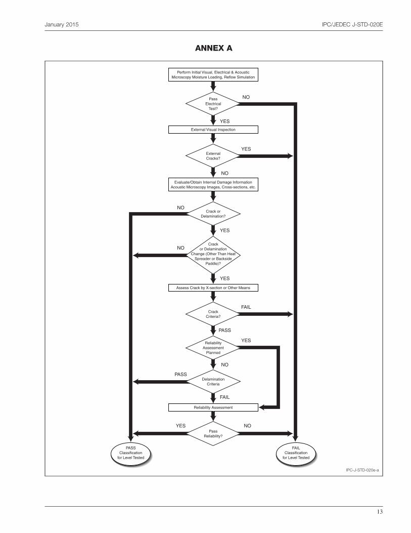
ANNEX A
IPC-J-STD-020e-a
Perform Initial Visual, Electrical & AcousticMicroscopy Moisture Loading, Reflow Simulation
Crackor Delamination
Change (Other Than HeatSpreader or Backside
Paddle)?
Evaluate/Obtain Internal Damage InformationAcoustic Microscopy Images, Cross-sections, etc.
Assess Crack by X-section or Other Means
Reliability Assessment
External Visual Inspection
PassElectrical
Test?
ExternalCracks?
Crack orDelamination?
CrackCriteria?
ReliabilityAssessment
Planned
DelaminationCriteria
PassReliability?
FAILClassification
for Level Tested
NO
YES
FAIL
YES
YES
NO
NO
NO
PASS
YES NO
YES
YES
PASS
NO
FAIL
PASSClassification
for Level Tested
January 2015 IPC/JEDEC J-STD-020E
13
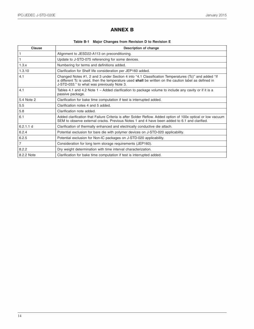
ANNEX B
Table B-1 Major Changes from Revision D to Revision E
Clause Description of change
1 Alignment to JESD22-A113 on preconditioning.
1 Update to J-STD-075 referencing for some devices.
1.3.x Numbering for terms and definitions added.
1.3.10 Clarification for Shelf life consideration per JEP160 added.
4.1 Changed Notes #1, 2 and 3 under Section 4 into ‘‘4.1 Classification Temperatures (Tc)’’ and added ‘‘Ifa different Tc is used, then the temperature used shall be written on the caution label as defined inJ-STD-033.’’ to what was previously Note 3.
4.1 Tables 4.1 and 4.2 Note 1 – Added clarification to package volume to include any cavity or if it is apassive package.
5.4 Note 2 Clarification for bake time computation if test is interrupted added.
5.5 Clarification notes 4 and 5 added.
5.8 Clarification note added.
6.1 Added clarification that Failure Criteria is after Solder Reflow. Added option of 100x optical or low vacuumSEM to observe external cracks. Previous Notes 1 and 4 have been added to 6.1 and clarified.
6.2.1.1 d Clarification of thermally enhanced and electrically conductive die attach.
6.2.4 Potential exclusion for bare die with polymer devices on J-STD-020 applicability.
6.2.5 Potential exclusion for Non-IC packages on J-STD-020 applicability.
7 Consideration for long term storage requirements (JEP160).
8.2.2 Dry weight determination with time interval characterization.
8.2.2 Note Clarification for bake time computation if test is interrupted added.
IPC/JEDEC J-STD-020E January 2015
14
Rev. 8/13
Standard Improvement Form JEDEC J-STD-020E The purpose of this form is to provide the Technical Committees of JEDEC with input from the industry regarding usage of the subject standard. Individuals or companies are invited to submit comments to JEDEC. All comments will be collected and dispersed to the appropriate committee(s). If you can provide input, please complete this form and return to:
JEDEC Attn: Publications Department 3103 North 10th Street Suite 240 South Arlington, VA 22201-2107
Fax: 703.907.7583
1. I recommend changes to the following: Requirement, clause number
Test method number Clause number
The referenced clause number has proven to be: Unclear Too Rigid In Error
Other
2. Recommendations for correction:
3. Other suggestions for document improvement:
Submitted by
Name: Phone:
Company: E-mail:
Address:
City/State/Zip: Date:
Association Connecting Electronic Industries
JEDEC Solid State Technology Association 3103 North 10th Street Suite 240S Arlington VA 22201 www.jedec.org
3000 Lakeside Drive, Suite 309 S Bannockburn, IL 60015 847-615-7100 tel 847-615-7105 fax www.ipc.org ISBN #978-1-61193-159-4