Embed Size (px)
Citation preview
Copyright © TWI Ltd 2008World Centre for Materials Joining Technology
Joined for LifeJoined for LifeStateState--ofof--thethe--art joining processes, from art joining processes, from chip interconnect to package sealingchip interconnect to package sealing
Developments in Interconnect, Developments in Interconnect, Assembly and Packaging WorkshopAssembly and Packaging Workshop
Helen Helen GoddinGoddin

Copyright © TWI Ltd 2008World Centre for Materials Joining Technology
Joining in MicroelectronicsJoining in Microelectronics•• TWI TWI MicrotechnologyMicrotechnology section deals with section deals with
joining, materials selection and design at all joining, materials selection and design at all levels of microelectronics manufacturelevels of microelectronics manufacture

Copyright © TWI Ltd 2008World Centre for Materials Joining Technology
OverviewOverviewWhat trends have there been for joining in microelectronics?
Copyright © TWI Ltd 2008World Centre for Materials Joining Technology
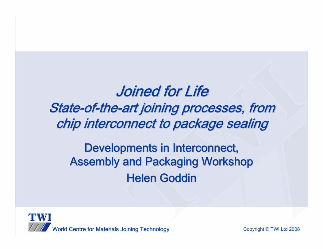
OverviewOverview
Wire bonding
Flip chip
Laser welding
Friction stir welding

Copyright © TWI Ltd 2008World Centre for Materials Joining Technology
OverviewOverview
Wire bonding
Flip chip
Laser welding
Friction stir welding
Reliability Testing
System in package

Copyright © TWI Ltd 2008World Centre for Materials Joining Technology
Joining Trends and IssuesJoining Trends and Issues•• MiniaturisationMiniaturisation
–– ManipulationManipulation–– Sensitivity to parametersSensitivity to parameters–– ReworkRework–– TestingTesting–– GeometryGeometry
•• LegislationLegislation•• New materialsNew materials•• Increasing automation and speedIncreasing automation and speed•• Thermal managementThermal management•• ReliabilityReliability

Copyright © TWI Ltd 2008World Centre for Materials Joining Technology
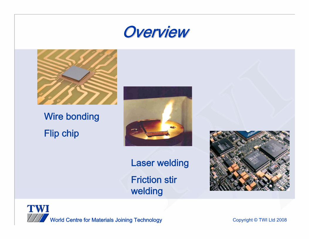
Wire bondingWire bonding•• Gold and aluminium wire bonding still makes Gold and aluminium wire bonding still makes
up large percentage of bonds made todayup large percentage of bonds made today•• Copper still of interest, some companies Copper still of interest, some companies
looking to put into manufacturelooking to put into manufacture•• Increased interest with Increased interest with
inin--situsitu monitoringmonitoring
Copyright © TWI Ltd 2008World Centre for Materials Joining Technology
Sensor
Digital Ultrasonic Generator
Actuator
• Mechanical Oscillations• Friction
PiQC-Signals
• Wire Deformation
• Current• Frequency
PiQCPiQC

Copyright © TWI Ltd 2008World Centre for Materials Joining Technology
Potential ApplicationsPotential Applications•• Identifying suspicious bonds (e.g. pad contamination, Identifying suspicious bonds (e.g. pad contamination,
scratches, misalignment)scratches, misalignment)•• Selecting conditions for fine wireSelecting conditions for fine wire
Contaminated bonds are represented by contours inside the map
Good bonds are located at the outer border of the map (100%)

Copyright © TWI Ltd 2008World Centre for Materials Joining Technology
Flip ChipFlip Chip
•• Use of flip chip projected to continue to growUse of flip chip projected to continue to grow•• Advantages:Advantages:
–– SizeSize–– PerformancePerformance–– FlexibilityFlexibility–– ReliabilityReliability–– Cost over other packaging methods.Cost over other packaging methods.–– Widening availability in flip chip materials, equipment, Widening availability in flip chip materials, equipment,
and servicesand services

Copyright © TWI Ltd 2008World Centre for Materials Joining Technology
Future ApplicationsFuture Applications•• OptoOpto--electronic devices.electronic devices.
•• XX--byby--wire automotive control systems. wire automotive control systems. ‘‘XX’’ represents the represents the basis of safetybasis of safety--related applications such as steering, related applications such as steering, braking, braking, powertrainpowertrain, suspension control, collision , suspension control, collision avoidance.avoidance.
•• High brightness LEDs are a potential future market for High brightness LEDs are a potential future market for flip chip. This will allow high currents and higher flip chip. This will allow high currents and higher brightness to be achieved.brightness to be achieved.
•• Digital TV marketDigital TV market

Copyright © TWI Ltd 2008World Centre for Materials Joining Technology
TWI and Flip ChipTWI and Flip Chip
•• Internal projects to assess technology Internal projects to assess technology •• Involvement in collaborative projects to support Involvement in collaborative projects to support
flip chip developmentflip chip development•• Prototyping for membersPrototyping for members
Bumped Silicon IC

Copyright © TWI Ltd 2008World Centre for Materials Joining Technology
TWI FacilitiesTWI Facilities•• BumpingBumping
–– stud bumpingstud bumping–– infrastructure evaluationinfrastructure evaluation–– bumping accessbumping access
•• Flip chip assemblyFlip chip assembly–– equipment evaluationequipment evaluation–– thermocompression thermocompression –– solder flip chipsolder flip chip–– adhesive flip chipadhesive flip chip–– process developmentprocess development–– device prototypingdevice prototyping
Soldered flip chip interconnection

Copyright © TWI Ltd 2008World Centre for Materials Joining Technology
Laser WeldingLaser Welding•• Well established in industry for Well established in industry for
package sealingpackage sealing•• Particularly titanium packages for Particularly titanium packages for
pacemakers and implantable pacemakers and implantable devicesdevices
•• Smaller spot size lasers now Smaller spot size lasers now availableavailable
•• Potential for welding leads on Potential for welding leads on packages (plated copper) dual packages (plated copper) dual wavelength lasers wavelength lasers
•• Aluminium alloy packages for Aluminium alloy packages for microwave applicationsmicrowave applications
•• Small thickness foils for electrical Small thickness foils for electrical interconnectionsinterconnections
GSI GSI LumonicsLumonicsNd:YAGNd:YAG
Welding/cuttingWelding/cutting

Copyright © TWI Ltd 2008World Centre for Materials Joining Technology
Micro Friction Stir Welding Micro Friction Stir Welding
TWI desktop TWI desktop μμFSW machineFSW machine2.5D CNC, 302.5D CNC, 30μμm accuracy, max m accuracy, max ωω = 24,000rpm, max = 24,000rpm, max νν = 6m/min= 6m/min

Copyright © TWI Ltd 2008World Centre for Materials Joining Technology
μμFSW AdvantagesFSW Advantages•• Exploit FSW for thin materials in:Exploit FSW for thin materials in:
–– electronics, photonics, automotive, aerospace, electronics, photonics, automotive, aerospace, consumer products, medical, power consumer products, medical, power …………
•• SingleSingle--pass, solidpass, solid--phase ambient joining phase ambient joining •• Environmentally and cleanroom friendlyEnvironmentally and cleanroom friendly
–– No chemical cleaningNo chemical cleaning–– No preNo pre--platingplating–– No added filler materialsNo added filler materials–– Low energy consumptionLow energy consumption
•• Fast, simple yet reliableFast, simple yet reliable•• Low capital with low consumablesLow capital with low consumables•• Efficient and low H&S riskEfficient and low H&S risk•• Small heat affected zoneSmall heat affected zone•• Unexplored potentialsUnexplored potentials
–– Metals, ceramics, plastics, compositesMetals, ceramics, plastics, composites–– Packaging, hermetic sealing, Packaging, hermetic sealing, microjoiningmicrojoining–– Butt, overlap & spot welding Butt, overlap & spot welding

Copyright © TWI Ltd 2008World Centre for Materials Joining Technology
Example application: Package sealingExample application: Package sealing
Fibre-optic receivers & transmitters
Copyright © TWI Ltd 2008World Centre for Materials Joining Technology
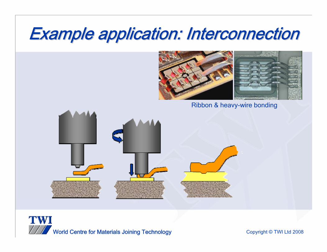
Example application: InterconnectionExample application: Interconnection
Ribbon & heavy-wire bonding

Copyright © TWI Ltd 2008World Centre for Materials Joining Technology
Reliability TestingReliability Testing•• Thermal cycling, thermal aging, Thermal cycling, thermal aging,
highly accelerated stress highly accelerated stress testing, power cyclingtesting, power cycling……..
•• Well established standards for Well established standards for different types of testing (e.g. different types of testing (e.g. JEDEC)JEDEC)

Copyright © TWI Ltd 2008World Centre for Materials Joining Technology
Reliability TestingReliability Testing•• Now emphasis on understanding Now emphasis on understanding
mechanisms of failure with minimum mechanisms of failure with minimum testing on smaller components testing on smaller components →→Precision Reliability Testing Precision Reliability Testing
•• Miniaturisation Miniaturisation →→ higher current higher current densities densities →→ electromigrationelectromigration in joints in joints as well as filmsas well as films

Copyright © TWI Ltd 2008World Centre for Materials Joining Technology
Al3Au8 AlAu2
AlAu4
Al3Au8
AlAu4voids Au
Au
Si
Si
voids
ElectromigrationElectromigration in Wire bondsin Wire bonds
AlAu2
AlAu4
Al3Au8
AlAu4Al3Au8
AlAu2
voids
voids
Si
Au
Au
Si
20μm

Copyright © TWI Ltd 2008World Centre for Materials Joining Technology
System in PackageSystem in Package
motherboard
Integrated passives
Active devices•• ADEPTADEPT--SiPSiP
Right first time design process
Copyright © TWI Ltd 2008World Centre for Materials Joining Technology
SummarySummary•• Joining continues to be one of the key Joining continues to be one of the key
challenges in microelectronics packaging challenges in microelectronics packaging •• Wire bonding inWire bonding in--situ monitoring important, situ monitoring important,
new new PiQCPiQC sold by sold by HesseHesse & & KnippsKnipps•• Lasers reducing in spot size, possible Lasers reducing in spot size, possible
applications in lead weldingapplications in lead welding•• Micro friction stir welding applications Micro friction stir welding applications
package sealing and lead weldingpackage sealing and lead welding•• ElectromigrationElectromigration in joints now importantin joints now important•• System in package design can maximise System in package design can maximise
board usage but must be board usage but must be ““right first timeright first time””