Embed Size (px)
Citation preview

John Spence Overview of electron diffraction. Erice June 9 2004.
1. Pulsed gas diffraction. LEED. RHEED. Photoelectron diffraction, holography.
2. Spot (SAD) patterns. Lattice, cell consts. Organics, inorganics Semi-quantitative TED + HREM. Examples from recent work of Dorset, Sinkler, Gjonnes, Zou et al.
3. CBED. Space-group determination, Cell constants, Strain mapping, Charge-density measurement, HV, Debye-Waller. Elastic filtering.
Quantitative
4. LACBED. CBIM. Dislocation Burger's vectors.
5. Coherent Nanodiffraction. Planar fault vectors. Ronchigrams for aligning corrected STEMs
6. Diffuse scattering. Phase transitions, phonons, defect analysis. Isolated nanostructures ? (Zuo's nanotube)
7. UHV TED from reconstructed surfaces of thin films. Quantitative
8. Cryomicroscopy in biology. (Most successful area of ED+Imaging). Solving proteins - organic monolayer xtals at 0.3nm resolution.
Quantitative
9. Phase identification Combine CBED (space group), SAD (lattice), EDX & ELS (composition).
10. Advanced topics. HiO inversion, Precession camera, Dynamical inversion, Ptychography, in-line STEM holography, imaging. ELNES + QCBED. Serial Xtallog - protein beam diffn.
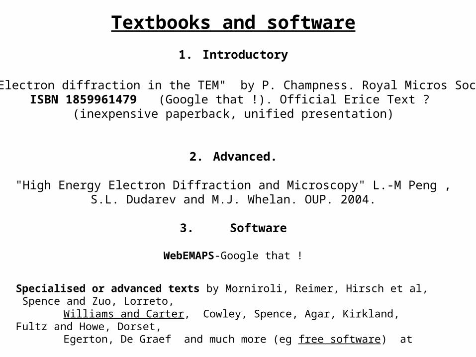
Textbooks and software
1. Introductory
"Electron diffraction in the TEM" by P. Champness. Royal Micros SocISBN 1859961479 (Google that !). Official Erice Text ?
(inexpensive paperback, unified presentation)
2. Advanced.
"High Energy Electron Diffraction and Microscopy" L.-M Peng , S.L. Dudarev and M.J. Whelan. OUP. 2004.
3. Software
WebEMAPS-Google that !
Specialised or advanced texts by Morniroli, Reimer, Hirsch et al, Spence and Zuo, Lorreto, Williams and Carter, Cowley, Spence, Agar, Kirkland, Fultz and Howe, Dorset,Egerton, De Graef and much more (eg free software) at
http://www.public.asu.edu/~jspence/ElectrnDiffn.html

Why is electron micro-diffraction a good idea ?
• It provides the strongest continuous signal from the smallest volume of matter known to science. Hence good for nanoscience.
• Field emission sources are the brightest continuous particle sources in physics.
• The interaction is the strongest of all the long-lived particles.Hence more signal.
• Ratio of elastic to inelastic scattering more favorable than X-rays (less damage for bio)
• TED is uniquely sensitive to ionicity.• The synthesis of many new nanostructured materials demands new
methods for structure analysis using nanoprobes.

Diffraction modes in the TEM/STEM.
S
1. Source conjugate to detector. SAD. 2. Source conjugate to sample. CBED.
Angular resolution limited by source size.Spatial resolution limited by SA aperture and Cs.
sampleSource image
S
SA apertureconjugate to sample
Source images.
sample
Fine detail in disks comes from outside probe ?Spatial resolution limited by probe size.

P
P'
Q
Q' P'P' Q'Q'
2 θB
B A
= X L g λ
Electron source
final condenser lens
2aperture C
- Probe forming lens
Electron probe
L
2 θB
θc
1. C2 may be coherently or incoherently filled.
2. CBED provides maximum info from smallest volume.
3. For refinement, strain mapping first - calibrate pattern.
4. We say that P’ and P’ are “conjugate points”.

SA Aperture
Virtual Aperture
Specimen
Lower ObjectiveLens Back Focal Plan
a) Selected Area Electron Diffraction
Specimen
nBack Focal Pla
ICondenser I
Upper Objective
Lower Objective
c) Convergent Beam Electron Diffraction
Upper Objective
Lower ObjectiveSpecimen
Condenser Lens III
C2 Aperture10µm
Back Focal Plane
b) Nanoarea Electron Diffraction
Fig. 1 Three modes of electron diffraction. Both a) selected area electron diffraction (SAED) and b) nanoarea electron diffraction (NED, Koehler) use parallel illumination. SAED limits the sample volume contributing to electron diffraction by using an aperture in the image plane of the image forming lens (objective). NED achieves a very small probe by imaging the condenser aperture on the sample using a third condenser lens (eg M= 1/20). Convergent beam electron diffraction (CBED) uses a focused probe.
PP’

Elementary electron diffraction and xtallography. Scattering geometry.
dhkl
θ
1/dhkl =sqrt(h^2 + k^2 +l^2)/a = θλ =|g|
for cubic system, cell const a.
Bragg's Law for HEED (small angle approx)
θ = 2θB = λ /dhkl where θ is the scattering angle.
Electron de-Broglie wavelength is
λ = 1.22643 / (V + 0.97845E-6 * V^2)1/2
with V the accelerating voltage, and λ in nm.
1/λ
g
Ewald sphere construction ensures conservation of energy, xtal momentum.
(But ! Apply uncertainty principle in beam dirn. for "elastic" scattering . t.Kz = 1, where t= thickness t.
Kz =Sg = 1/t
Hence expect strong Bragg beams for a small range of incident beam directions within excitation error Sg.)
Sg
θB

Find relative position of FOLZ projected ontoHOLZ. This gives centering. (eg I, body centered in recip space, fcc in real)
•From FOLZ ring we get c axis dimension. Sg = 1/c = λU2H/2
•From spot measurements get approx cell consts.
•More accurate Bravais lattice and cell consts can be obtained by method of Zuo Ultramic 52, 459 "A new method ofBravais Lattice determination" using HOLZ lines in central CBED disk.
Phase identification of unknown structures by CBED and SAD.
1. Find space-group by CBED.
2 Use EDX and ELS to determine atoms present and approximate stoichiometery. (Can Nb2O5 be distinguished from NbO2 by EDX ? Probably.
3. Find Bravais lattice from spot patterns with HOLZ ring. Use d=λL/R, L camera length, R spot radius.
ZOLZ
FOLZ
4. Use the indexed patterns given in Spence and Zuo book ?. (HOLZ points indicated on ZOLZ). OR:Simulate any pattern (WebEMAPS-Google that !) with random atom posns in known space group.
5 Use Electron Diffraction data base: http://www.nist.gov/srd/nist15.htm and/or Powder Diffraction File.
uH
Sg
g
FOLZ

NIST Standard Reference Database 15
NIST/Sandia/ICDD Electron Diffraction Database
Designed for phase characterization obtained by electron diffraction methods, this database and associated software permit highly selective identification procedures for microscopic and macroscopic crystalline materials.
The database contains chemical, physical, and crystallographic information on a wide variety of materials (over 81,534) including minerals, metals, intermetallics, and general inorganic compounds.
The Electron Diffraction Database has been designed to include all the data required to identify materials using computerized d-spacing/formula matching techniques. The data for each entry include:
* the conventional cell
* reduced cell
* lattice type
* space group
* calculated or observed d-spacings
* chemical name
* chemical and empirical formula
* material class indicators
* references. . .
This database and search software are available in magnetic tape format and in CD-ROM format.
Can one Google a set of d spacings ?
(Try it now for Si on wireless web)

ΘΒ
α
K K
Κt
α
g
Sg
Bragg
Off Bragg
A
B
g/2
0
RC
Figure 2 Two Ewald sphere orientations differing by α , just off (continuous lines) and on(dashed lines) the Bragg condition. Note the direction of Kt. The excitation error is Sg.
Sg ≈ 2θBα/ λ ≈ gα
Ewald sphere in more detail…
We can associate an excitationerror (in Ang-1) with every Braggbeam in a TED pattern.
The Bragg condition corresponds to Sg = 0.
In the zone-axis (symmetric)
orientation, the excitation error is
Sg = λ g2 / 2
FT
t
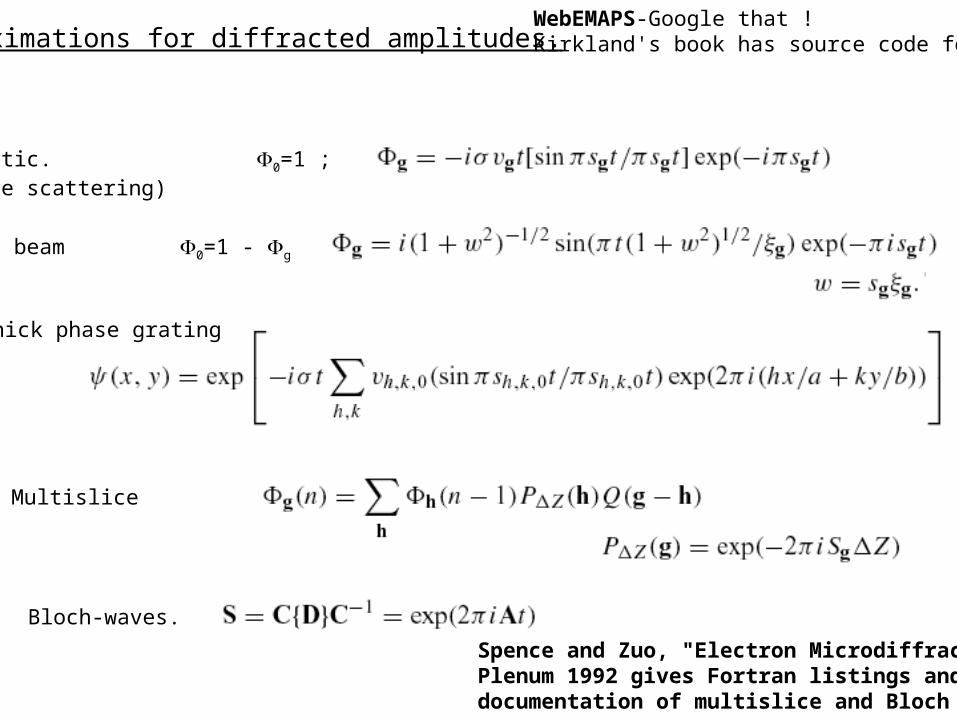
Approximations for diffracted amplitudes.WebEMAPS-Google that !Kirkland's book has source code for ms
Kinematic. 0=1 ;(single scattering)
Two beam 0=1 - g
Thick phase grating
Multislice
Bloch-waves.
Spence and Zuo, "Electron Microdiffraction"Plenum 1992 gives Fortran listings and fulldocumentation of multislice and Bloch wave.


Lynch, Moodie, O'KeeffeActa A31, 300
Comparison of N-beam, PGA, kinematic approx. for NbO
Exact (N-beam)
PGA
Kinematic
Phase
Amplitude, not intensity.
kin
PGA=FT {exp(i(R)t)}
Kin=Vg t sin(Sgt)/(Sgt)
Note: kin intensity goes as t2
Dyn intens is "sinusiodal".kin phase is linear.X-ray amplitudes don’t involvet at all !
Conclude: Need t < 8 nm Inorg t < 20 nm Org
Layer structures help (projection)
Thickness

At x1 (b), central beam is strongImage consists mainly of interferencebetween central beam and eachbeam, producing a faithful image.
Failure of kinematic approx.
000
111
At x5 (c), central beam is weak.Image consists mainly of interferencebetween beams, producing an imageof half-spacings, and rotated.
Increasing thickness
Thickness (A)
Kinematic ~ t2
000

E x p
T h e o r y
0
5 0 0
1 0 0 0
1 5 0 0
2 0 0 0
2 5 0 0
Figure 5. A comparison of experimental (dots) and calculated intensity (arbitrary units) alongthe line drawn in figure 3 for the elastically filtered Si (111) systematic Bragg reflections. Withthis agreement between theory and experiment it is possible to measure structure factors to anaccuracy of 0.1% in the most favorable cases, which is suffi cient to directly observe the bondsin the resulting charge-density map of a crystal.
How do we know thesemultiple-scattering calcnsare accurate ?
Because they precisely fitexperimental data, as here.(Zuo J. Elec Mic 47, 121)
Figure 3. Silicon (111) systematics at 196.15 kV. The bright disc is (000). Fine HOLZ lines canbe seen running parallel to the straight line drawn across all the disks, for which the intensity isshown in figure 5.

MgO (111) systematics CBED fitted at 120 kV using elastic imaging energy filter. (Zuo 97)
Conclusion: Accurate quantificationof ED data is only possible if multiplescattering is included in calculations
But…. for light-element inorganicnanostuctures, kinematic theory is accurate enough to solve structuresespecially if good data can be obtained in 3D !
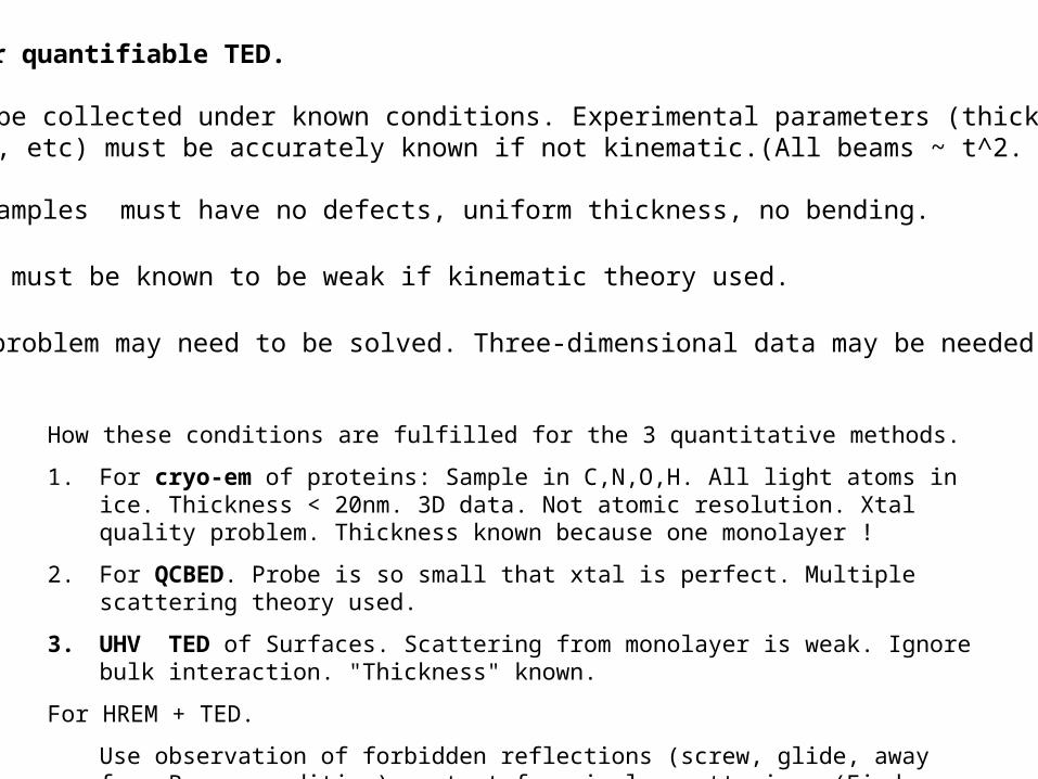
Conditions for quantifiable TED.
1. Data must be collected under known conditions. Experimental parameters (thickness, wavelength, etc) must be accurately known if not kinematic.(All beams ~ t^2. Normalise)
2. Xtalline samples must have no defects, uniform thickness, no bending.
3. Scattering must be known to be weak if kinematic theory used.
4. Phase problem may need to be solved. Three-dimensional data may be needed.
How these conditions are fulfilled for the 3 quantitative methods.
1. For cryo-em of proteins: Sample in C,N,O,H. All light atoms in ice. Thickness < 20nm. 3D data. Not atomic resolution. Xtal quality problem. Thickness known because one monolayer !
2. For QCBED. Probe is so small that xtal is perfect. Multiple scattering theory used.
3. UHV TED of Surfaces. Scattering from monolayer is weak. Ignore bulk interaction. "Thickness" known.
For HREM + TED.
Use observation of forbidden reflections (screw, glide, away from Bragg condition) as test for single scattering. (Find space-group by CBED to indicate which are forbidden ?). At Bragg, forbiddens remain forbidden (black cross) even if dynamical.

Tests for kinematic scattering.
1. Use Friedel's law. If a crystal is known to be acentric, but I(g) = I(-g), there is no multiple scattering. (for acentrics, Vg = V-g*, but V(r) is real). This works for unknown structures.
2. Blank discs. If the intensity variation across CBED discs is constant, this suggests weak scattering. (Wu, Spence Acta A58, 580. "Kinematic and dynamical CBED for solving thin organic films at helium temperature. Tests with anthracene").
3. Study organic monolayers. Thickness equals known molecular size. Problem - make self-supporting sample ! (eg use ice). Poor sample quality. LB films- mols lie on side.
4. Use wedge-shaped sample. Match image against thickness. Similar for CBED.
5. Inclined, planar-fault on known plane can be used to give thickness on wedge.
6. Accurate fitting to CBED pattern with multiple scattering program will calibrate thickness within < 4 A
7. Find space-group by CBED to locate true forbiddens* (use primitive cell),index pattern. Then forbidden reflections in SAD from thin, bent areas suggest no multiple scattering.
8. Credibility requires the same structure to be determined from the same sample by XRD and TED ! Are the TED intensities consistent and reproducible ? Can you record the same set of TED diffracted intensities twice, from different areas of the same sample ?Remember- modern XRD software always gives some answer ! (R factor ?Potl vs Rho).
(*screw, glide)

Elementary Xtallography.
Xtal = Bravais lattice + molecule.
•There are only 14 possible Bravais lattices, s.t. the surroundings of every point are identical.
•Seven primitive cells exist (seven xtal systems :cubic, hexagonal, triclinic ,monoclinic, orthorom, tetragonal, trigonal )
•Get 7 more from centering, P, I, F, C. (primitive, body-centered, centered on every face, centered on two)
•The xtal system is defined by the symmetry of the xtal. (eg any xtal with four 3-folds is cubic).
•From the cell constants a,b,c, α the reciprocal lattice is generated by FT. eg a* = b X c /.
•The point group is based on mirror, inversion, and rotation symetries alone. There are 32. (eg for mols).
•Translational symmetry adds the possibility of screw and glide symmetries. There are 230 space groups.
•There are 2 types of truly forbidden reflections - Space group (screw,glide axes). Non-spherical atoms.Third type "forbidden" due to centering is historical artifact, due to method of indexing*. Use primitive cell !The f'bdns generated by a centered cell were never there ! Physically, electrons diffract from the primitive cell.
•Choice of cell is not unique. Primitive cell contains one lattice point - no forbiddens, all indices occur.
•Friedel's law. I(g) = I(-g). Holds only if kinematic (eg X-rays). Not if multiple scattering. Adds 1 symmetry.
A list of absent refln indices due to centering, screw, glide, and many indexed patterns (including HOLZ) is given in Spence and Zuo, Electron Microdiffraction, 1992 . Plenum. Use Int Tables for Crystallography.
*centering was used to give orthogonal coords.

Solutions to the phase problem.
If diffraction patterns can be collected under kinematic conditions, we must solve phase problem. (Phases can be obtained from FT of HREM image if wpo approx holds. +/- if centric).
Modern PX used MAD. (Heavy atom, abs. Most proteins don’t diffract to atomic resolution)
Modern inorganic xtallog uses Direct Methods, requires atomic resolution data, <1000 (?) atoms.
Then the powerful atomicity constraint can be used. Recently, the simple "charge flipping"algorithm has been developed. ( Oszlanyi and Suto, Acta A60, p.134 (2004) )
Recently the phase problem for continuous scattering from non-periodic objects has been solvedexperimentally with electrons and X-rays by new iterative methods. ("lensless imaging")see - Weierstall et al Ultramic 90, 171 and Zuo et al Science 300, p. 1419 for electrons and Marchesini et al Phys Rev B68 (140101) (2003) for soft X-rays.
These iterative algorithms are developed from work by Fienup, Gerchberg, Saxton and others.
If you use XRD software for TED data, be aware of two important differences between XRD and TED data:1. For XRD, all reflections are collected at the Bragg condition. Not so for zone-axis TED.2. For XRD, reflections are angle-integrated. Not so for TED or, usually, CBED.

A new algorithm for xtal phase problem: "Charge flipping" Oszlányi Acta A60 134, '04.
1. Start with measured |Fhkl|, random phases.
2. Transform.
3 Set Im()=0. Find x~20% of largest positive , keep them. (Support estimate)
4 Reverse sign (flipping) of all other (r) below threshold x.
5. Go to 2.
1
R factor
Iteration number
*Unlike direct methods does not need known scatt factors !
*flipping finds support !
*Converges to same structureindep of initial phases.
x was reduced here
C6Br6 exptl data
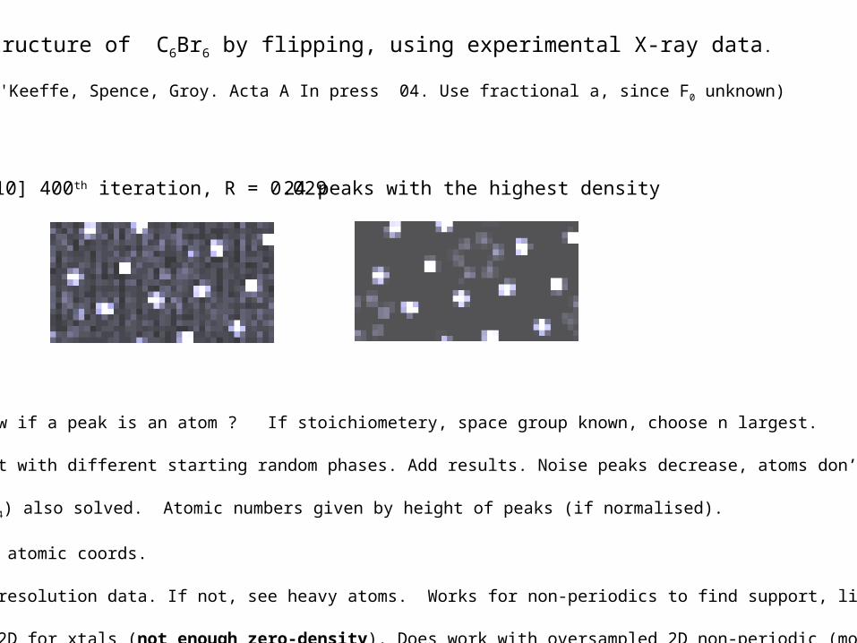
Solve structure of C6Br6 by flipping, using experimental X-ray data.
(Wu, O'Keeffe, Spence, Groy. Acta A In press 04. Use fractional a, since F0 unknown)
[010] 400th iteration, R = 0.029 24 peaks with the highest density
•How do we know if a peak is an atom ? If stoichiometery, space group known, choose n largest.
•If not, repeat with different starting random phases. Add results. Noise peaks decrease, atoms don’t.
•Dioxane (SnBr4) also solved. Atomic numbers given by height of peaks (if normalised).
•Gives correct atomic coords.
•Needs atomic resolution data. If not, see heavy atoms. Works for non-periodics to find support, like shrinkwrap.
•Wont work in 2D for xtals (not enough zero-density). Does work with oversampled 2D non-periodic (more zero density)

Imaging theory - needed because collection of 3D diffraction data is difficultFlipping doesn’t work in 2D (and requires atomic resolution data).
Electron beam
Oops ! Double diffraction
Inside sample
Exit-face wavefunction(may be dynamical)
Abbe interpretation.
Exit-face wave Diffraction pattern Image.
1. For a perfect lens, image is magnified copy of exit face wave-function.
2. This is a faithful representation of the projected potential only if kinematic, and flat Ewald sphere.(wpo)
3. FT of such an exit face wave wave gives "structure factors" Vg. propn to diff. pattern spot intensities.
4. If multiple scattering inside sample, FT of exit face wave still gives d.p. But spots are not stucture factors.
(Lens phase shift)

Electron/specimen interaction: refraction with locally varying index:
Incident wave. Plane of constant phase is flat.
Exit wave: Phase front has wobble
{sample
+ ++
++
++ +
+ + ++
+ ++
+
+ +++
1
-i
Representation on argand diagram: Wave has a range of phase values In kinematic theory, phase is 90o wrt (000)
kin
(000)
electrons go faster along atoms,with higher kinetic energy, shorterwavelength, more wiggles.

The dynamical exit-face wave.
plane wave
Diffraction pattern(Not structure factors !)
Exit face wavefunction(Not faithful projection. Correct period)
Image
FT
plane wave
Diffraction pattern(Structure factors)
Exit face wavefunction(Faithful projection)
Image(copy of exit face wavefunction)
FTKinematic scattering
Multiple (dynamic) scattering
Note: FT relationship between exit face and diffraction pattern is preserved with multiple scattering
Thin !
Thick !

HREM imaging theory for weak phase objects.
Exit face wavefield
Weak scattering
Diffracted amplitude
Add lens, aperture
Image amplitude
Image intensity
Notes: dark atoms predicted on bright background at Scherzer focus, where - 90 degree lens phase-shiftadds to - 90 degree scattering phase (i = exp i /2). Then replace P(u,v) exp() in 4 by -i to give imageI(x,y) = 1 - 2 p(-x,-y) for ideal lens without aperture.
4

85 pmAluminum Oxygen
Kisielowski et al NCEM LBL Ultram 2001.
High contrast - not a weak phase object !
WPO Not WPO
"Multiple scattering is the usual condition in electron diffraction"
1Intensity in image
A B
Contrast = A/B must be small for WPO.
Position


Diffractograms for wpo. Finding structure factor phases from HREM images.
The complex Fourier transform of the WPO image intensity can be obtained in a computer as
where D, C are constants. Hence if is known, the phase of the fourier coefficients of the projected potential can be found. These phases are 0 or 180 degrees (wrt some origin) for centric projections
where
2

From "HREM" by JCHS, 3rd Edn 2003. OUP

Solving structures from point electron diffraction patterns alone.
Examples. 1. Inorganic.
• Weirich et al. Acta A56, p.29 (2000). Ti2Se Octahedra. Short b axis along beam.Direct Methods.SIR97 SAD patterns from areas thin enough to show no forbiddenreflections. Symmetry related merging. Assume |Fhkl|~Ihkl for "extinction" model. (Cowley 1992). Unlike XRD, peak heights in potential map are not proportional to atomic number. Note: xtal thickness neither known nor enters analysis. No corrections for Ewald sphere curvature. EDX used for stoichiometry. R=24%. Film, CCD. Five other fine-grained structures solved. Atom position error 0.2 Ang.

Solving structures from point electron diffraction patterns alone.
Examples. 2. Organics (Proteins are another story !) Dorset. Acta A54, p. 750 (1998). Linear chain polymers require view normal to chain - difficult ! Caprolactane was xtallized in two orientations. Direct methods. Solved.
Example 3. The precession camera. (Vincent and Midgely 1994, Marks 03 JMCFest., Gjonnes et al 1998). AlmFe intermetallic. Patterson and Direct Methods. 3D. No short axis. Precession data is "more kinematic" since angle-integrated.(Direct beam precesses around ZOLZ).
Blackman, 1939 gives angle-integrated 2-beam soln. Ig ~ |Ug|2 t for small t, but remarkably Ig ~ |Ug| for large t. Structure solved with 3 Fe and 12 Al atoms.
Definition of R factor:
R=
{g∑ Fg
obs −Fgcalc}
Fgobs
g∑

Solving xtal structures by combining HREM images and TED patterns.
Example: Inorganic. Zou et al. Acta A59, p.526 (2003).
AlCrFe. 3D "quasixtal". a=4nm !. 13 different TED Zones. 124 atoms found. FilmWPO assumed, and HREM images corrected for defocus, Cs. Phases obtained from these.Magnitudes from TED patterns. Some projections are centro. Xtal is not. Symmetry merging.CRISP used. No correction for Ewald sphere curvature. (Same method as proteins). No thickness

BeO (wurtzite) CBED down c. 100kV . Elastic imaging filter. Sixfold axis. Projection diffraction group 6mm1R
Space-group determination by CBED.
1. Find point group hence crystal system (cubic, hexagonal, trigonal, tetragonal, orthorhombic, monoclinic, triclinic).
2. Find Bravais lattice and centering. Index.
3. Find screw and glide elements. Find space group by adding these translational symmetries to the point group laid down at every point of Bravais lattice.

QuickTime™ and aVideo decompressor
are needed to see this picture.

Dynamically forbidden reflections in BeO (hexagonal, wurtzite) shows 21 (contained in 63 ) screw axis along c and/or c glide axis.
c
Bragg condition is along line B
from Zuo and Spence, Microdiffraction, Plenum, 92

0
1 10-12
2 10-12
3 10-12
4 10-12
5 10-12
6 10-12
7 10-12
0 0.5 1 1.5
f (cm)
s (1/angstrom)
0
1 10 -8
2 10 -8
3 10 -8
4 10 -8
5 10 -8
6 10 -8
7 10 -8
0 0.5 1 1.5
f (cm)
s (1/angstrom) -2 10 -12
-1 10 -12
0
1 10 -12
2 10 -12
0 0.5 1 1.5
f (cm)
s (1/angstrom)
s=1/2
s=-1/2
Electrons X-ray Neutronsf s( ) = v(r)exp(4πis⋅r)dr∫
=2.38×10⁻¹⁰ λsinθ
⎛ ⎝
⎞ ⎠
2
Z−f x( )
f x s( ) =e2
moc2 ρ(r)exp(4πis⋅r)dr∫
=2.82×10⁻¹³f xb=bc +2bi I I +1( )[ ]
−1/ 2s⋅I
Mn3+ Mn3+ Mn
Compared to X-rays and Neutrons, Electrons• Interact strongly with matter• Have bright source• Are very sensitive to charge states at small scattering angles• Are scattered predominantly by nuclei at high scattering angles• Have the smallest probe ~1 Å
Electrons, X-rays and Neutrons
Jim Zuo/MATSE

Figure 8(b). Measured surfaces of constant charge density difference in Cu2O along the(vertical) copper-oxygen bond. Blue shows less charge than MCDF ions (producing adz^2 "hole"), red is more.
(cf Tanaka, Tsuda, Saunders, Bird, Nufer, Mayer, Fox…) .
Seeing Bonds

FIG 1.—Elastic filtered [001] TED pattern from Si
at 120 KV and 105oK showing TDS from phonon modes. Contour map (log. scale) around spot (-6,6,0) from image plate (IP). Filtered, 120 kV,
105oK.
FIG 2.—Line trace from IP along [-1,-1,0],through (-6,6,0)
FIG 3.—[-1,-1,0] scan through (-6,6,0), line 1 in FIG.2, and [-1,1,0], line 2. Backgroundsubtracted.
(-4,8,0)
(-4,4,0)
(-8,4,0)
(-8,8,0)
(-6,6,0)
1
2
Figure 1
[-1,-1,0]
TED of diffuse scattering from phonon modes in silicon - beyond the Einstein model.
Hoier, Kim, Zuo, Spence Shindo, MSA 95
I(q,) = e.g q-2 -2 for these transverse acoustic modes phonones, where e (along [-1,1,0],[1,1,0]) is phonon polarization, q (along [110],[-1,1,0]) is phonon wavevectorand phonon freq.
Recorded in Koehler mode at 105K on Fuji Image Plates

Diffuse scattering in Magnetite at metal-insulator Verwey transition (about 120K).a) 130K b)326 K. Inset: (800) left (880) right.
Elastically filtered scattering recorded using Image Plates. (Leo Omega 912).
*Zuo, Pacaud, Hoier, Spence. Micron, 31, p. 527 (2000).
a b
(000)
(400)
(220)
The atomic mechanism of metal-insulator phase transition in Magnetite*

129 K 154 K 184 K 386 K
p
v
Temperature dependence of diffuse around (800) Bragg spots compared with theory for polaron (Yamada).

The monoclinic cell of our low temperature charge ordering model (model 2, B-sites only).The yellow tetrahedrons (molecular polarons) form a linked chain with alternating opposite dipoles (red arrows). The chains are separated by molecular polarons of different orientations (blue). The left shows the schematic arrangement of the spiral chains (shown as bars)
above and below Verwey transition.
Fe
Fe2+
3+
0<T-T v< ~180
am a c+
b c
bm -ac+bc
c m
2c c
90.2° T-Tv< 0

J.M.Zuo et al Science 300, 1420 (2003).
First atomic-resolution diffractive image reconstruction.
SAD TEM
Double-walled Nanotube
Image reconstructed from electron-diffraction pattern by HiO
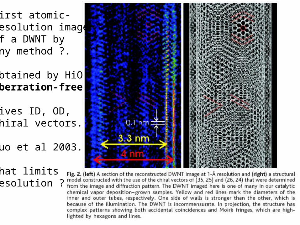
First atomic-resolution imageof a DWNT by any method ?.
Obtained by HiO.Aberration-free.
Gives ID, OD,Chiral vectors.
Zuo et al 2003.
What limitsresolution ?

The challenge of electron crystallography.
*To collect three-dimensional diffraction data under kinematic conditions.Then not restricted to short c axis. Note: centers of each CBED disc in a small-probe pattern provide a point pattern ! Blank disks suggest single-scattering conditions.
*To solve the same unknown structure first by TED and then by XRD, get same result.
In the age of nanoscience, there is an urgent need for a method of rapidly solving new , inorganic nanostructured materials. Many are fine-grained, light element, crystalliteswhich cannot be solved by XRD. The unsolved challenge of 50 years is…..
The difficulties are
•Goniometers. Loss of area during tilt.
•Contamination
•Automation of tilt and data collection.
•Radiation damage.
GO TO http://www.public.asu.edu/~jspence/ElectrnDiffn.htmlFor free software ! Useful books, papers, group web pages , conferences etc !!!!! OR Google IUCr

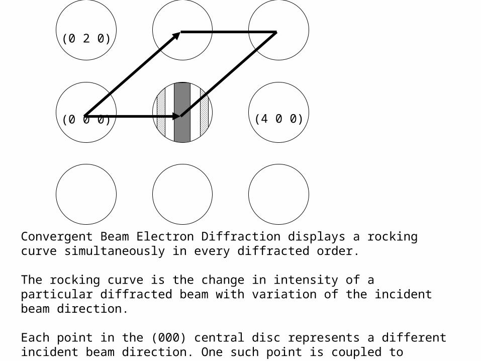
(0 0 0)
(0 2 0)
(4 0 0)
Convergent Beam Electron Diffraction displays a rocking curve simultaneously in every diffracted order.
The rocking curve is the change in intensity of a particular diffracted beam with variation of the incident beam direction.
Each point in the (000) central disc represents a different incident beam direction. One such point is coupled to conjugate points in all the other discs differing by reciprocal lattice vectors.

Dynamically forbidden reflections.
- - + +
+ + - -
o o o
oo
h
k
20 21 22 23
02
Y'Y
XX
ZZ'
A
B
A
Gjonnes and Moodie, Acta A19, p. 65 (1965).
Scattering paths arranged in pairs which cancel on black lines, cross, for all thickness and voltage !Black cross appears on disk at Bragg condition. Black lines on other kinematically forbiddens
Screw axis along c, k. Alternate reflections along c extinguished kinematically.
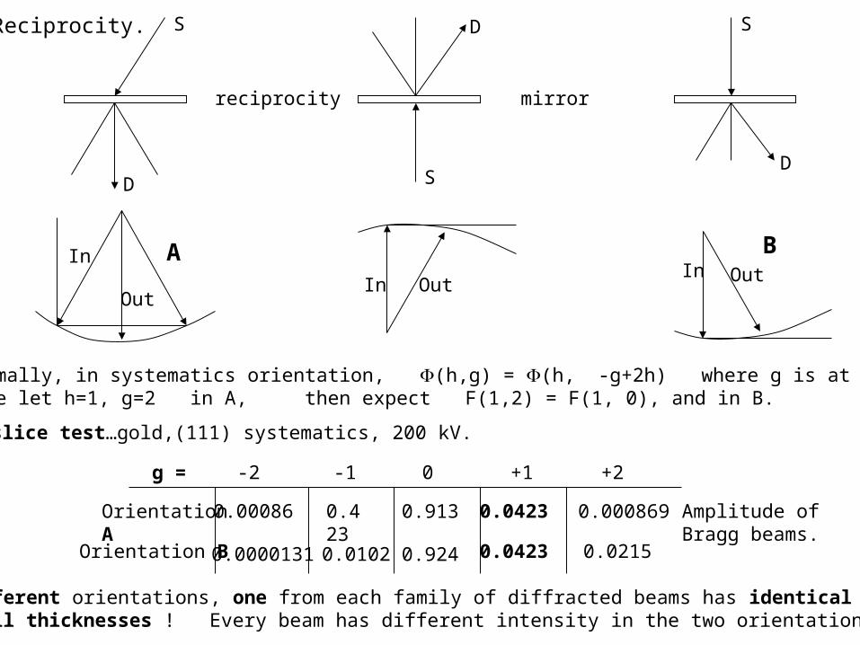
Reciprocity. S
In
Out
D S
D
mirrorreciprocity
In OutIn Out
S
D
Formally, in systematics orientation, (h,g) = (h, -g+2h) where g is at Bragg.Here let h=1, g=2 in A, then expect F(1,2) = F(1, 0), and in B.
A B
-2 -1 0 +1 +2
0.00086 0.423 0.913 0.0423 0.000869
0.0000131 0.0102 0.924 0.0423 0.0215
g =
Orientation A
Orientation B
Amplitude of Bragg beams.
In these two different orientations, one from each family of diffracted beams has identical complex amplitudeThis holds for all thicknesses ! Every beam has different intensity in the two orientations, except +1 !
Multislice test…gold,(111) systematics, 200 kV.