Embed Size (px)
Citation preview
JESD204B Start Up: Configuration Requirements and Debug
October 2012
JESD204B System Start Up
• This app note provides an overview of a JESD204B system start up.
The document discusses clocking scheme, timing and configuration of
JESD204B devices for various subclasses. It also discusses some of
the possible debugging techniques to troubleshoot JESD204B high
speed serial interface. Basic understanding of JESD204B standard is
expected.
Clocking & Timing Signals
• In JESD204B, clocking scheme and timing signal may vary depending upon the subclass and
whether multi-device synchronization is required. The relationship between clock and timing
signals become even more crucial in subclass 1 & 2 which support deterministic latency.
JESD204B has the flexibility of having mismatched track lengths for data lanes due to lane
alignment mechanism. However synchronization across multiple converter devices and
deterministic latency depends strongly upon how accurately phase relationship between
various clock and timing signals is controlled.
• Regardless of the subclass, device clocks going to different converters must be phase aligned.
Device clock is the common clock and any mismatch in it would directly affect synchronization
among multiple converter devices.
• Clocking scheme and timing signals for each JESD204B subclass is discussed below. Note
that there is always some tolerable skew margin in the generation/distribution of timing signals.
Refer to section 4.12 of JESD204B standard.
Subclass 1
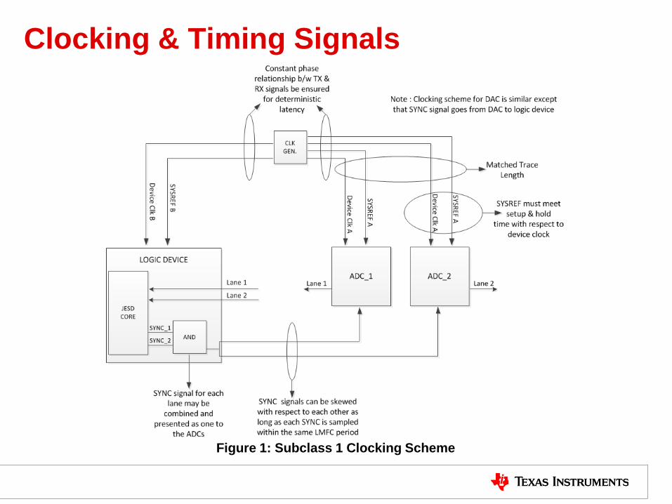
• Figure 1 in the next slide shows the clock and timing signals as well as necessary relationship
between them. The figure is drawn for the case of two converter devices linked to a single logic
device with one lane to each converter. Similar clocking scheme will be applied to any number
of converters/lanes in a JESD204B system.
• Device clocks for different converters should be phase and frequency aligned.
Clocking & Timing Signals
Figure 1: Subclass 1 Clocking Scheme
Clocking & Timing Signals
Subclass 1 (cont’d)
• Device clocks across two sides of the link i.e. between TX and RX need not to be aligned. However their
should be a deterministic phase relationship between them. Any variation in their relative phase would add to
variation in the link latency (see Figure 6 at the end of the document). It is for this reason advisable to use a
single clock source to generate all the clocks in JESD204B system.
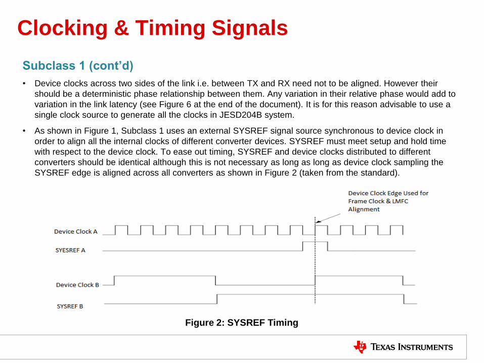
• As shown in Figure 1, Subclass 1 uses an external SYSREF signal source synchronous to device clock in
order to align all the internal clocks of different converter devices. SYSREF must meet setup and hold time
with respect to the device clock. To ease out timing, SYSREF and device clocks distributed to different
converters should be identical although this is not necessary as long as long as device clock sampling the
SYSREF edge is aligned across all converters as shown in Figure 2 (taken from the standard).
Figure 2: SYSREF Timing
Clocking & Timing Signals
Subclass 1 (cont’d)
• SYSREF can be a one-shot, gapped periodic or a periodic signal. Incase of periodic or gapped periodic, period of the SYSREF must be integer multiple of the Local Multi Frame Clock (LMFC) in order to avoid SYSREF pulse in the middle of a multiframe.
• Since a periodic SYSREEF signal acts as a sub-harmonic clock of the converter sampling clock and may have spurious effect on the converter performance, it may be turned off during normal operation once synchronization has been achieved in which case, TX and RX devices must have the ability to generate a “Generate SYSREF” request to the clock generator whenever a synchronization request is detected at the SYNC interface.
• There should be a known delay between when SYSREF is sampled high in TX and RX in order to have constant phase relationship between LMFCs on the two sides of the link. As mentioned earlier, this can be ensured by having a constant phase between TX and RX device clocks and generating SYSREF for TX and RX at the same time (or with a constant delay) using a single clock source. This is done to avoid uncertainty in the link latency (see Figure 6 at the end of the document).
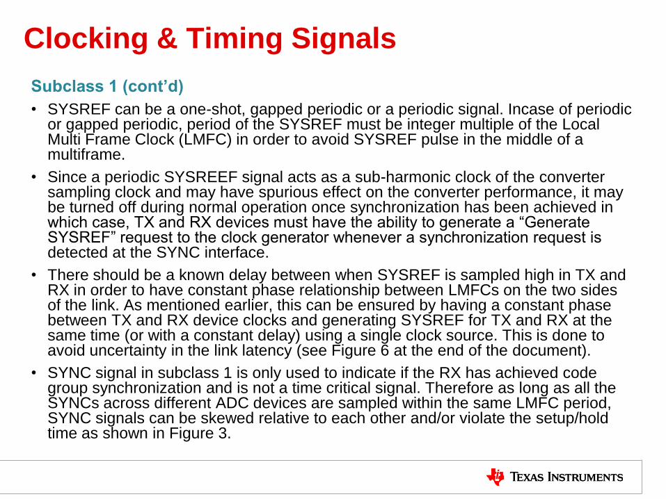
• SYNC signal in subclass 1 is only used to indicate if the RX has achieved code group synchronization and is not a time critical signal. Therefore as long as all the SYNCs across different ADC devices are sampled within the same LMFC period, SYNC signals can be skewed relative to each other and/or violate the setup/hold time as shown in Figure 3.
Clocking & Timing Signals
Subclass 1 (cont’d)
• In the case of multiple DAC devices, SYNC signal from each DAC
device may be combined before sending to TX logic device.
Figure 3: Skew in SYNC Sampling
Clocking & Timing Signals
Subclass 2
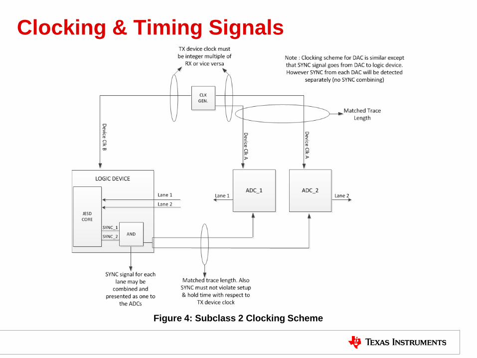
• Figure 4 in the next slide shows the clock and timing signals as well as necessary relationship between them for subclass 2. The figure is drawn for the case of two converter devices linked to a single logic device with one lane to each converter. Similar clocking scheme will be applied to any number of converters/lanes in a JESD204B system.
• As with subclass 1, device clock across multiple converter devices must be aligned with each other.
• Subclass 2 requires TX and RX device clocks be integer multiple of each other. This is to ensure that SYNC meets setup and hold time at the TX with respect to TX device clock.
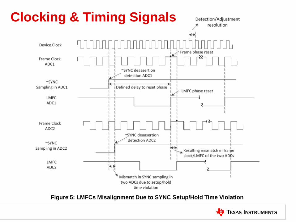
• Subclass 2 relies on SYNC signal to align multiple converters and achieve deterministic latency. Hence timing of SYNC signal must be accurately controlled. Trace length of all SYNC signals for different converter devices must be matched and system must be designed such that there is no timing violation with respect to TX device clock. As shown in Figure 5 in slide ahead, any setup/hold time violation would result in misalignment of LMFCs across different converter devices and would introduce uncertainty in the link latency.
• As shown in Figure 5, as per standard, a subclass 2 ADC device must specify a known delay between the sampling of SYNC assertion and phase reset of internal clocks. This delay needs to be constant in order to maintain a constant phase relationship between LMFCs across either side of the link (i.e. between TX and RX LMFCs). As discussed in subclass 1, this constant phase relationship is necessary in order to avoid uncertainty in the link latency . See Figure 6 at the end of document to see resulting variation in the link latency due to variation in the phase relationship between TX and RX LMFCs.
Clocking & Timing Signals
Figure 4: Subclass 2 Clocking Scheme
Clocking & Timing Signals
Figure 5: LMFCs Misalignment Due to SYNC Setup/Hold Time Violation
Clocking & Timing Signals
Subclass 2 (cont’d)
• In the case of subclass 2 DAC, SYNC signal carries phase information of DAC LMFC. Hence combining multiple SYNC signals in the logic device from different DAC devices is not allowed. SYNC signal from each DAC must be sent separately to the TX logic device so that LMFC phase of each DAC can be detected by the logic device.
• Note that subclass 2, in absence of a source synchronous SYSREF signal, relies on a system synchronous approach whereby the system must be designed to meet setup and hold time of SYNC signal at TX. Such type of timing control is quite difficult to achieve at higher speeds. Hence if an external timing signal can be made available, subclass 1 approach should be preferred to ease timing control. As suggested in the standard, subclass 1 should always be used for sampling rates above 500MSPS.
Subclass 0
• Clocking scheme of subclass 0 is similar to that of subclass 2 with the exception of timing requirements on the SYNC signal. Incase of subclass 0, there is no support for deterministic latency as well as synchronization across multiple converter devices is optional. Hence discussion on SYNC signal timing in subclass 2 applies in subclass 0 only when multi-device synchronization is needed.
• Also in the case of subclass 0 TX logic device , there is no mechanism to detect LMFC phase of different DAC devices. Hence if multiple DAC synchronization is needed, a separate inter-RX device synchronization needs to be implemented in order to align internal clocks across different DAC devices. Standard leaves the implementation of this standard up to designer, however the interface should be synchronous to the frame clock.
Device Configuration
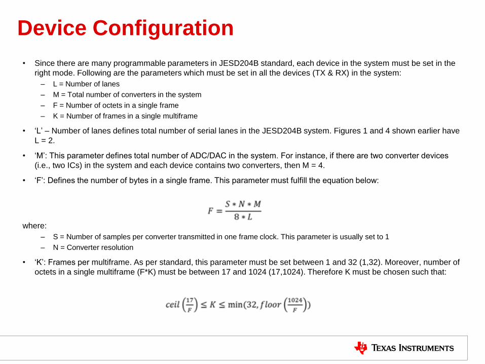
• Since there are many programmable parameters in JESD204B standard, each device in the system must be set in the
right mode. Following are the parameters which must be set in all the devices (TX & RX) in the system:
– L = Number of lanes
– M = Total number of converters in the system
– F = Number of octets in a single frame
– K = Number of frames in a single multiframe
• „L‟ – Number of lanes defines total number of serial lanes in the JESD204B system. Figures 1 and 4 shown earlier have
L = 2.
• „M‟: This parameter defines total number of ADC/DAC in the system. For instance, if there are two converter devices
(i.e., two ICs) in the system and each device contains two converters, then M = 4.
• „F‟: Defines the number of bytes in a single frame. This parameter must fulfill the equation below:
where:
– S = Number of samples per converter transmitted in one frame clock. This parameter is usually set to 1
– N = Converter resolution
• „K‟: Frames per multiframe. As per standard, this parameter must be set between 1 and 32 (1,32). Moreover, number of
octets in a single multiframe (F*K) must be between 17 and 1024 (17,1024). Therefore K must be chosen such that:
Device Configuration
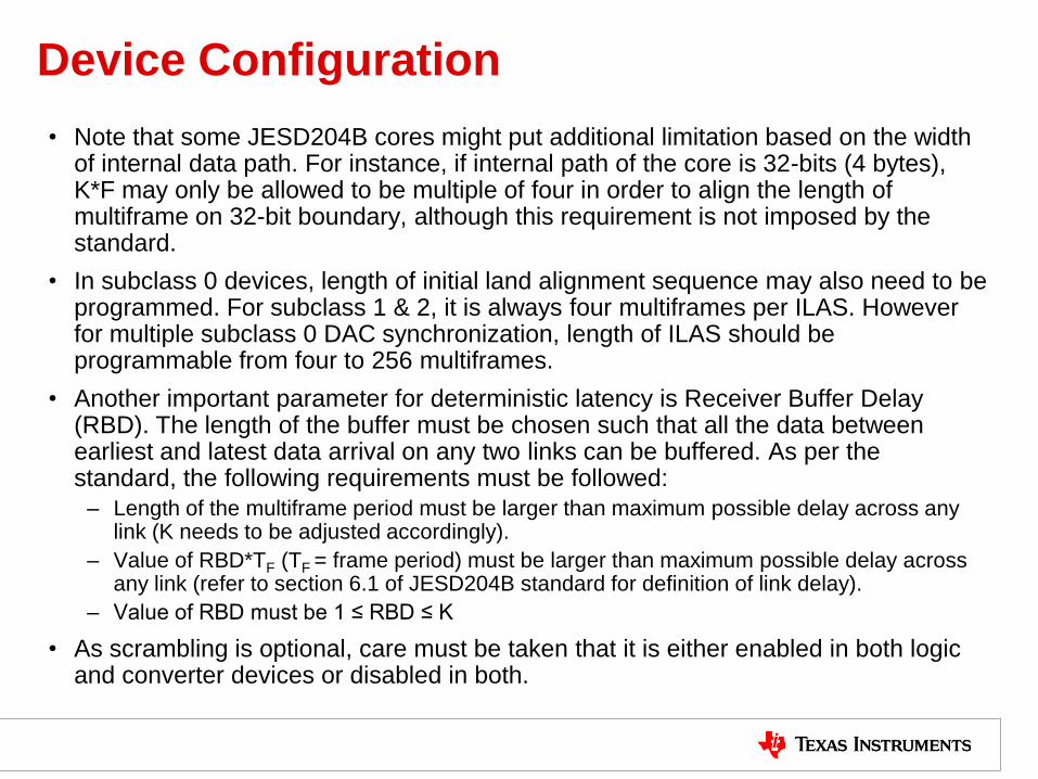
• Note that some JESD204B cores might put additional limitation based on the width of internal data path. For instance, if internal path of the core is 32-bits (4 bytes), K*F may only be allowed to be multiple of four in order to align the length of multiframe on 32-bit boundary, although this requirement is not imposed by the standard.
• In subclass 0 devices, length of initial land alignment sequence may also need to be programmed. For subclass 1 & 2, it is always four multiframes per ILAS. However for multiple subclass 0 DAC synchronization, length of ILAS should be programmable from four to 256 multiframes.
• Another important parameter for deterministic latency is Receiver Buffer Delay (RBD). The length of the buffer must be chosen such that all the data between earliest and latest data arrival on any two links can be buffered. As per the standard, the following requirements must be followed:
– Length of the multiframe period must be larger than maximum possible delay across any link (K needs to be adjusted accordingly).
– Value of RBD*TF (TF = frame period) must be larger than maximum possible delay across any link (refer to section 6.1 of JESD204B standard for definition of link delay).
– Value of RBD must be 1 ≤ RBD ≤ K
• As scrambling is optional, care must be taken that it is either enabled in both logic and converter devices or disabled in both.
JESD204B Debugging
• As JESD204B is a serial interface running up to 12.5Gbps with no clock sent with the data, debugging can
be a bit challenging.
• To start with, visual indication can be used to monitor following on the logic device:
– Transceiver Lock : Indicates if the transceiver PLLs are locked to the input clock
– SYNC Assertion : A visual indication of SYNC signal should be used to see if code group synchronization has been
achieved.
– Data Valid : In the case of RX logic device, data valid signal from the JESD core can be used to indicate the reception
of parallel user data at the output of receiver.
• Care should be taken about polarity of the SYNC signal. As per JESD204B standard, SYNC is an active
low signal. Hence when RX is out of synchronization, SYNC is set to logic „1‟ and after synchronization
SYNC is set to logic „0‟. Make sure both TX and RX devices treat SYNC as an active low else polarity of
SYNC needs to be inverted.
• In case of periodic or gapped periodic SYSREF for subclass 1, it should be checked that SYSREF period
is whole multiple of multiframe period otherwise synchronization can not be achieved.
• As samples are mapped into octets over different lanes, data will be corrupted if mapping is different in TX
and RX. To test transport layer mapping, JESD204B specifies transport layer test pattern whereby
receiver matches received samples with the expected pattern and indicates the result. As per the standard
both TX and RX devices must support this test mode.
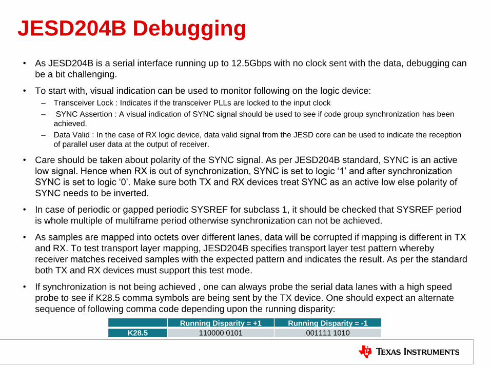
• If synchronization is not being achieved , one can always probe the serial data lanes with a high speed
probe to see if K28.5 comma symbols are being sent by the TX device. One should expect an alternate
sequence of following comma code depending upon the running disparity:
Running Disparity = +1 Running Disparity = -1
K28.5 110000 0101 001111 1010
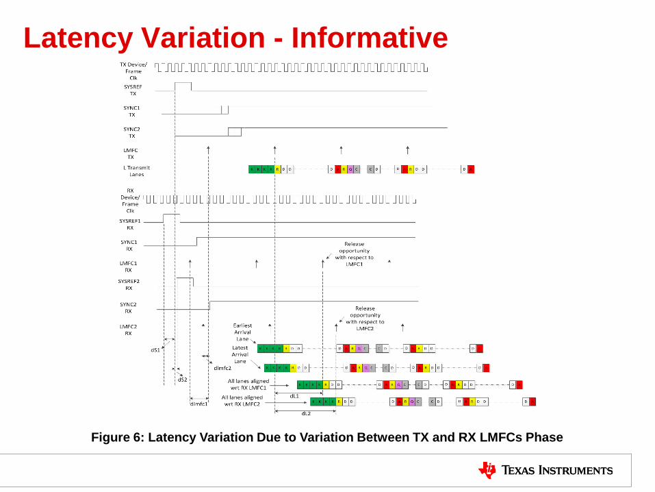
Latency Variation - Informative
• This is an informative section describing how the change in the relative phases of TX and RX LMFCs cause variation in the link latency as shown in Figure 6. The timing diagram has been drawn for subclass 1 however a similar argument is applied for subclass 2 operation except that SYNC acts as timing signal to align LMFCs.
• In subclass 1, SYSREF acts as a timing signal and the edge of the device clock at which SYSREF is sampled high is used to align LMFCs across different converter devices. As per the standard, delay between SYSREF sampled high and phase reset of LMFC should be constant for the device.
• Figure 6 shows „SYSREF TX‟ signal which resets the phase of internal clocks in the transmitter and generate „LMFC TX‟ edge. Similarly „SYSREF1 RX‟ signal which resets the phase in the receiver and generates „LMFC1 RX‟. The relative phase difference between the LMFC TX and LMFC1 RX is marked as „dlmfc1‟. The resulting link latency is marked as „dL1‟.
• „SYSREF2 RX‟ shows a shifted version of SYSREF1 RX. The relative phase difference between LMFC TX and „LMFC2 RX‟ (receiver LMFC generated with respect to SYSREF2 RX) is „dlmfc2‟ and the resulting link latency is „dL2‟.
• As can be seen, as the relative phase difference between LMFCs of TX and RX changes (dlmfc1-dlmfc2), it results in the variation of latency (dL2-dL1). Therefore it is necessary to maintain a constant phase relationship between the LMFCs of TX and RX to avoid change in the link latency.
• As can be noted from the figure, in order to maintain a constant phase relationship between TX and RX LMFC, SYSREF of TX and RX should be launched with a constant delay with respect to each other every time synchronization is required.
• A similar variation in the latency will occur if instead of SYSREF, there is a change in the phases between TX and RX device clocks. Therefore, in order to minimize uncertainty in the link latency, there should always be a constant relationship between the TX device clock/sysref and RX device clock/sysref.
Latency Variation - Informative
Figure 6: Latency Variation Due to Variation Between TX and RX LMFCs Phase
IMPORTANT NOTICE
Texas Instruments Incorporated and its subsidiaries (TI) reserve the right to make corrections, enhancements, improvements and otherchanges to its semiconductor products and services per JESD46, latest issue, and to discontinue any product or service per JESD48, latestissue. Buyers should obtain the latest relevant information before placing orders and should verify that such information is current andcomplete. All semiconductor products (also referred to herein as “components”) are sold subject to TI’s terms and conditions of salesupplied at the time of order acknowledgment.
TI warrants performance of its components to the specifications applicable at the time of sale, in accordance with the warranty in TI’s termsand conditions of sale of semiconductor products. Testing and other quality control techniques are used to the extent TI deems necessaryto support this warranty. Except where mandated by applicable law, testing of all parameters of each component is not necessarilyperformed.
TI assumes no liability for applications assistance or the design of Buyers’ products. Buyers are responsible for their products andapplications using TI components. To minimize the risks associated with Buyers’ products and applications, Buyers should provideadequate design and operating safeguards.
TI does not warrant or represent that any license, either express or implied, is granted under any patent right, copyright, mask work right, orother intellectual property right relating to any combination, machine, or process in which TI components or services are used. Informationpublished by TI regarding third-party products or services does not constitute a license to use such products or services or a warranty orendorsement thereof. Use of such information may require a license from a third party under the patents or other intellectual property of thethird party, or a license from TI under the patents or other intellectual property of TI.
Reproduction of significant portions of TI information in TI data books or data sheets is permissible only if reproduction is without alterationand is accompanied by all associated warranties, conditions, limitations, and notices. TI is not responsible or liable for such altereddocumentation. Information of third parties may be subject to additional restrictions.
Resale of TI components or services with statements different from or beyond the parameters stated by TI for that component or servicevoids all express and any implied warranties for the associated TI component or service and is an unfair and deceptive business practice.TI is not responsible or liable for any such statements.
Buyer acknowledges and agrees that it is solely responsible for compliance with all legal, regulatory and safety-related requirementsconcerning its products, and any use of TI components in its applications, notwithstanding any applications-related information or supportthat may be provided by TI. Buyer represents and agrees that it has all the necessary expertise to create and implement safeguards whichanticipate dangerous consequences of failures, monitor failures and their consequences, lessen the likelihood of failures that might causeharm and take appropriate remedial actions. Buyer will fully indemnify TI and its representatives against any damages arising out of the useof any TI components in safety-critical applications.
In some cases, TI components may be promoted specifically to facilitate safety-related applications. With such components, TI’s goal is tohelp enable customers to design and create their own end-product solutions that meet applicable functional safety standards andrequirements. Nonetheless, such components are subject to these terms.
No TI components are authorized for use in FDA Class III (or similar life-critical medical equipment) unless authorized officers of the partieshave executed a special agreement specifically governing such use.
Only those TI components which TI has specifically designated as military grade or “enhanced plastic” are designed and intended for use inmilitary/aerospace applications or environments. Buyer acknowledges and agrees that any military or aerospace use of TI componentswhich have not been so designated is solely at the Buyer's risk, and that Buyer is solely responsible for compliance with all legal andregulatory requirements in connection with such use.
TI has specifically designated certain components which meet ISO/TS16949 requirements, mainly for automotive use. Components whichhave not been so designated are neither designed nor intended for automotive use; and TI will not be responsible for any failure of suchcomponents to meet such requirements.
Products Applications
Audio www.ti.com/audio Automotive and Transportation www.ti.com/automotive
Amplifiers amplifier.ti.com Communications and Telecom www.ti.com/communications
Data Converters dataconverter.ti.com Computers and Peripherals www.ti.com/computers
DLP® Products www.dlp.com Consumer Electronics www.ti.com/consumer-apps
DSP dsp.ti.com Energy and Lighting www.ti.com/energy
Clocks and Timers www.ti.com/clocks Industrial www.ti.com/industrial
Interface interface.ti.com Medical www.ti.com/medical
Logic logic.ti.com Security www.ti.com/security
Power Mgmt power.ti.com Space, Avionics and Defense www.ti.com/space-avionics-defense
Microcontrollers microcontroller.ti.com Video and Imaging www.ti.com/video
RFID www.ti-rfid.com
OMAP Applications Processors www.ti.com/omap TI E2E Community e2e.ti.com
Wireless Connectivity www.ti.com/wirelessconnectivity
Mailing Address: Texas Instruments, Post Office Box 655303, Dallas, Texas 75265Copyright © 2012, Texas Instruments Incorporated