Embed Size (px)
Citation preview
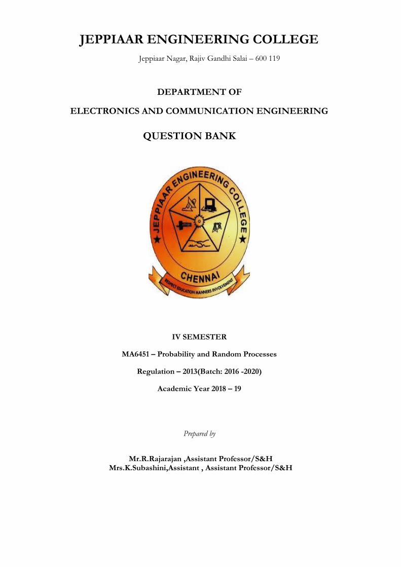
JEPPIAAR ENGINEERING COLLEGE
Jeppiaar Nagar, Rajiv Gandhi Salai – 600 119
DEPARTMENT OF
ELECTRONICS AND COMMUNICATION ENGINEERING
QUESTION BANK
IV SEMESTER
MA6451 – Probability and Random Processes
Regulation – 2013(Batch: 2016 -2020)
Academic Year 2018 – 19
Prepared by
Mr.R.Rajarajan ,Assistant Professor/S&H Mrs.K.Subashini,Assistant , Assistant Professor/S&H
JEPPIAAR ENGINEERING COLLEGE
Jeppiaar Nagar, Rajiv Gandhi Salai – 600 119
DEPARTMENT OF ELECTRONICS AND COMMUNICATION ENGINEERING
QUESTION BANK
SUBJECT : EC6404 – Linear Integrated Circuits
YEAR /SEM: II /IV
UNIT I :BASICS OF OPERATIONAL AMPLIFIERS
Current mirror and current sources, Current sources as active loads, Voltage sources, Voltage References, BJT
Differential amplifier with active loads, Basic information about op-amps – Ideal Operational Amplifier - General
operational amplifier stages -and internal circuit diagrams of IC 741, DC and AC performance characteristics, slew
rate, Open and closed loop configurations.
PART-A
CO Mapping : C213.1
Q.NO Questions BT
Level Competence PO
1.
Draw the dc transfer characteristics of a BJT
differential amplifier and define differential mode
input voltage
BTL-3 Applying PO1
2. Write down the characteristics of ideal operational
amplifier? BTL-4 Analyzing PO1
3. Why is the current mirror circuit used in differential
amplifier stages? BTL-2 Understanding PO1
4. Differentiate the ideal and practical characteristics of
an op-amp BTL-3 Analyzing PO1
5. Draw the circuit diagram of a symmetrical emitter
coupled differential amplifier. BTL-3 Applying PO1
6. Draw the Internal Block diagram of Op – Amp BTL-3 Applying PO1
7.
An operational amplifier has a slew rate of 4v/µs
.Determine the maximum frequency of operation to
produce distortion less output swing of 12V
BTL-6 Creating PO1,PO2
8. What is the cause for slew rate and how it can be
made faster? BTL-2 Understanding PO1.PO2.PO3
9. Define input bias current and input offset current of
an operational amplifier BTL-1 Remembering PO1
10.
A differential amplifier has a differential voltage gain
of 2000 and a common mode gain of 0.2.Determine
the CMRR in dB
BTL-6 Creating PO1,PO2
11. Define Slew rate and what causes slew rate? BTL Remembering PO1
12. Define CMRR of an operational amplifier? BTL Remembering PO1
13. What is current mirror? BTL-2 Understanding PO1
14. Explain the limitation of current mirror circuits? BTL-2 Understanding PO1
15. Draw the circuit of a Widlar current source and write
the exp for its output current BTL-3 Applying PO1
16. Define Thermal Drift BTL-1 Remembering PO1
17. What is an operational amplifier? BTL-2 Understanding PO1
18. What are the AC characteristics of an op-amp? BTL-2 Understanding PO1
19. What are the DC characteristics of an op-amp? Give
the typical values for an IC741? BTL-2 Understanding PO1,PO2
20. When does the op-amp behave as a switch? BTL-2 Understanding PO1
21.
In response to square wave input, the output of an op-
amp changed from –3V to +3V over a time interval
of 0.25μs. Determine the slew rate of the op-amp.
BTL-6 Creating PO1,PO2,
22. Define integrated circuit. BTL-1 Remembering PO1
23. What are the advantages of integrated circuits over
discrete components? BTL-2 Understanding PO1
24. What are the disadvantages of integrated circuits? BTL-2 Understanding PO1
25. What is meant by monolithic IC BTL-2 Understanding PO1
26. What are the two requirements to be met for a good
current source? BTL-2 Understanding PO1,PO2
27. List the various methods of realizing high input
resistance in a differential amplifier BTL-2 Understanding PO1
28. Mention two advantages of active load over passive
load in an operational amplifier BTL-4 Analyzing PO1
29. What is active load? Where it is used and why? BTL-2 Understanding PO1
30. Define supply voltage rejection ratio (SVRR) BTL-1 Remembering PO1,PO2
31. Define input offset voltage BTL-1 Remembering PO1
32. Define Frequency Response BTL-1 Remembering PO1
33. Define unity gain bandwidth of a Op-Amp BTL-1 Remembering PO1
PART B &C
Q.NO Questions BT
Level Competence
PO
1.
i)With a help of a block diagram ,explain the various
stages present in an operational amplifier
ii)Draw the transfer characteristics of an operational
amplifier and explain the linear and non-linear
operation
BTL-2
BTL-3
Understanding
Applying
PO1
PO1
2.
i)What is the input and output voltage and current
offsets? How are they compensated?
ii) With neat diagram derive the AC performance
close loop characteristics of Op-Amp to discuss on
the circuit Bandwidth, Frequency response and slew
rate
BTL-2
BTL-3
Understanding
Applying
PO1
PO1,PO2
3.
i)With a schematic diagram, explain the effect of RE
on CMRR in differential amplifier
ii)Discuss about the methods to improve CMRR
BTL-2
BTL-3
Understanding
Applying
PO1
PO1
4.
i)With simple schematic of differential amplifier
explain the function of Operational Amplifier
ii)Briefly Explain about constant current source
BTL-2
BTL-2
Understanding
Understanding
PO1
PO1
5.
i)Briefly explain the techniques used for frequency
compensation
ii)How do the open loop gain and the closed loop gain
of an op-amp differ?
BTL-2
BTL-2
Understanding
Understanding
PO1
PO1
6. With a neat diagram Explain the input side of the
internal circuit diagram of IC741 BTL-2 Understanding PO1
7.
What is the need for frequency compensation in an
OPAMP? With a suitable illustration, explain the
pole-zero frequency compensation technique.
BTL-2
Understanding
PO1
8. Draw the circuit of basic current mirror and explain BTL-3 Applying PO1
its operation. Also discuss about how current ratio
can be improved in the basic current mirror. Sketch
the improved circuit and explain
9.
i)Define and explain slew rate. What is full power
bandwidth? Also explain the method adopted to
improve slew rate
ii)Define output off set voltage. Explain methods to
nullify offset voltage
BTL-2
BTL-2
Understanding
Understanding
PO1
PO1
10. Explain in detail wilson current source and widlar
current source and derive necessary equations BTL-2 Understanding
UNIT II : APPLICATIONS OF OPERATIONAL AMPLIFIERS
Sign Changer, Scale Changer, Phase Shift Circuits, Voltage Follower, V-to-I and I-to-V converters, adder,
subtractor, Instrumentation amplifier, Integrator, Differentiator, Logarithmic amplifier, Antilogarithmic amplifier,
Comparators, Schmitt trigger, Precision rectifier, peak detector, clipper and clamper, Low-pass, high-pass and
band-pass Butterworth filters.
PART-A
CO Mapping : C213.2
Q.NO Questions BT
Level Competence
PO
1. State the limitations of an ideal integrator. BTL-1 Remembering PO1
2. How will you realize a peak detector using a precision
rectifier? BTL-5 Evaluating PO1
3. What is the need for converting a first order filter into
a second order filter? BTL-2 Understanding PO1
4. How is the current characteristic of a PN junction
employed in a Log amplifier? BTL-5 Evaluating PO1
5.
For the op-amp shown in figure determine the voltage
gain
BTL-6 Creating PO1,PO2
6. Draw the circuit diagram of a peak detector with
waveforms. BTL-3 Applying PO1
7. Give any four applications of comparators. BTL-1 Remembering PO1
8. What is hysteresis and mention the purpose of
hysteresis in a comparator? BTL-2 Understanding PO1
9. What is the difference between normal rectifier and
precision rectifier? BTL-2 Understanding PO1
10.
Plot the transfer characteristics of the circuit shown in
figure 2 .The op-amp saturates at +/-12V
BTL-3 Applying PO1,PO2
11. Define inverting amplifier and draw the circuit? BTL-1 Remembering PO1
12. Define non-inverting amplifier and draw the circuit? BTL-1 Remembering PO1
13. What is meant by voltage follower? BTL-2 Understanding PO1
14. Draw the circuit diagram of an op-amp integrator.
Mention its applications BTL-3 Applying PO1
15. Draw the circuit diagram of an op-amp differential
amplifier. Mention its o/p equation BTL-3 Applying PO1
16. For the op-amp shown in figure, determine the
voltage gain. BTL-3 Applying PO1
17. Explain the voltage to current convertor
BTL-2 Understanding
PO1
18. Draw the circuit of a voltage follower using op-amp
and prove that its gain is exactly equal to unity BTL-3 Applying PO1
19.
An ac signal has got a magnitude of 0.1 volt peak to
peak. Suggest a suitable half wave rectifier for this
signal. BTL-4 Analyzing PO1,PO2
20. Derive the expression for voltage gain of an inverting
operational amplifier? BTL-5 Evaluating PO1
21. Mention two linear and two non- linear operations
performed by an operational amplifier? BTL-4 Analyzing PO1
22. Explain the current to voltage convertor? BTL-2 Understanding PO1
23. Mention two application of Schmitt trigger? BTL-4 Analyzing PO1
24. Mention the characteristics of Instrumentation
amplifier? BTL-4 Analyzing PO1
25. State the disadvantages of passive filters? BTL-2 Understanding PO1
26. What is Precision rectifier? BTL-2 Understanding PO1
27. Define precision half wave rectifier with diagram? BTL-1 Remembering PO1
28. What are the main drawbacks of ideal differentiator? BTL-2 Understanding PO1
29. What are the steps to be followed while designing a
good differentiator? BTL-2 Understanding PO1
30. What are the main drawbacks of ideal integrator
circuit? BTL-2 Understanding PO1
31. Give the output voltage when Vi is positive and
negative in a precision diode. BTL-3 Applying PO1
32. Give an application of an Inverting Amplifier BTL-3 Applying PO1
33. Draw the circuit diagram of a schmitt trigger BTL-3 Applying PO1,PO2
34. Draw the circuit diagram of differentiators and give
its output equation BTL-3 Applying PO1,PO2
35.
Determine the output voltage for the circuit shown in
figure 1 when
(a)Vin=-2V
(b)Vin=3V
BTL-6 Creating PO1,PO2
PART:B & C
Q.NO BT
Level Competence
PO
1.
i)For performing differentiation in an operational
amplifier, integrator is preferred to differentiator-
Explain
ii) What is instrumentation amplifier? Draw a system
whose gain is controlled by a variable resistance
BTL-2
BTL-3
Understanding
Applying
PO1
PO1
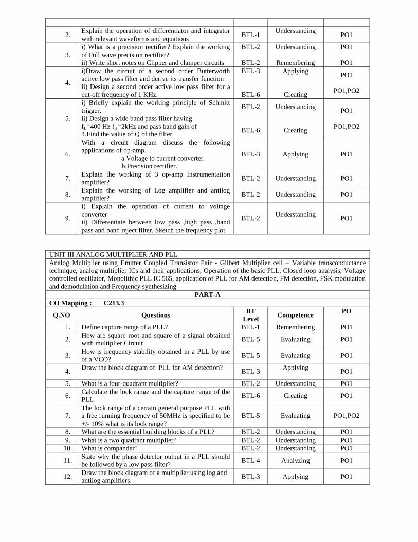
2. Explain the operation of differentiator and integrator
with relevant waveforms and equations BTL-1
Understanding
PO1
3.
i) What is a precision rectifier? Explain the working
of Full wave precision rectifier?
ii) Write short notes on Clipper and clamper circuits
BTL-2
BTL-2
Understanding
Remembering
PO1
PO1
4.
i)Draw the circuit of a second order Butterworth
active low pass filter and derive its transfer function
ii) Design a second order active low pass filter for a
cut-off frequency of 1 KHz.
BTL-3
BTL-6
Applying
Creating
PO1
PO1,PO2
5.
i) Briefly explain the working principle of Schmitt
trigger.
ii) Design a wide band pass filter having
fL=400 Hz fH=2kHz and pass band gain of
4.Find the value of Q of the filter
BTL-2
BTL-6
Understanding
Creating
PO1
PO1,PO2
6.
With a circuit diagram discuss the following
applications of op-amp.
a.Voltage to current converter.
b.Precision rectifier.
BTL-3 Applying PO1
7. Explain the working of 3 op-amp Instrumentation
amplifier? BTL-2 Understanding PO1
8. Explain the working of Log amplifier and antilog
amplifier? BTL-2 Understanding PO1
9.
i) Explain the operation of current to voltage
converter
ii) Differentiate between low pass ,high pass ,band
pass and band reject filter. Sketch the frequency plot
BTL-2 Understanding
PO1
UNIT III ANALOG MULTIPLIER AND PLL
Analog Multiplier using Emitter Coupled Transistor Pair - Gilbert Multiplier cell – Variable transconductance
technique, analog multiplier ICs and their applications, Operation of the basic PLL, Closed loop analysis, Voltage
controlled oscillator, Monolithic PLL IC 565, application of PLL for AM detection, FM detection, FSK modulation
and demodulation and Frequency synthesizing
PART-A
CO Mapping : C213.3
Q.NO Questions BT
Level Competence
PO
1. Define capture range of a PLL? BTL-1 Remembering PO1
2. How are square root and square of a signal obtained
with multiplier Circuit BTL-5 Evaluating PO1
3. How is frequency stability obtained in a PLL by use
of a VCO? BTL-5 Evaluating PO1
4. Draw the block diagram of PLL for AM detection?
BTL-3 Applying
PO1
5. What is a four-quadrant multiplier? BTL-2 Understanding PO1
6. Calculate the lock range and the capture range of the
PLL BTL-6 Creating PO1
7.
The lock range of a certain general purpose PLL with
a free running frequency of 50MHz is specified to be
+/- 10% what is its lock range?
BTL-5 Evaluating PO1,PO2
8. What are the essential building blocks of a PLL? BTL-2 Understanding PO1
9. What is a two quadrant multiplier? BTL-2 Understanding PO1
10. What is compander? BTL-2 Understanding PO1
11. State why the phase detector output in a PLL should
be followed by a low pass filter? BTL-4 Analyzing PO1
12. Draw the block diagram of a multiplier using log and
antilog amplifiers. BTL-3 Applying PO1
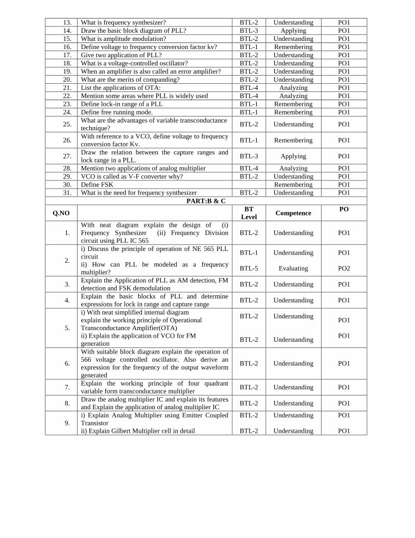
13. What is frequency synthesizer? BTL-2 Understanding PO1
14. Draw the basic block diagram of PLL? BTL-3 Applying PO1
15. What is amplitude modulation? BTL-2 Understanding PO1
16. Define voltage to frequency conversion factor kv? BTL-1 Remembering PO1
17. Give two application of PLL? BTL-2 Understanding PO1
18. What is a voltage-controlled oscillator? BTL-2 Understanding PO1
19. When an amplifier is also called an error amplifier? BTL-2 Understanding PO1
20. What are the merits of companding? BTL-2 Understanding PO1
21. List the applications of OTA: BTL-4 Analyzing PO1
22. Mention some areas where PLL is widely used BTL-4 Analyzing PO1
23. Define lock-in range of a PLL BTL-1 Remembering PO1
24. Define free running mode. BTL-1 Remembering PO1
25. What are the advantages of variable transconductance
technique? BTL-2 Understanding PO1
26. With reference to a VCO, define voltage to frequency
conversion factor Kv. BTL-1 Remembering PO1
27. Draw the relation between the capture ranges and
lock range in a PLL. BTL-3 Applying PO1
28. Mention two applications of analog multiplier BTL-4 Analyzing PO1
29. VCO is called as V-F converter why? BTL-2 Understanding PO1
30. Define FSK Remembering PO1
31. What is the need for frequency synthesizer BTL-2 Understanding PO1
PART:B & C
Q.NO BT
Level Competence
PO
1.
With neat diagram explain the design of (i)
Frequency Synthesizer (ii) Frequency Division
circuit using PLL IC 565
BTL-2 Understanding PO1
2.
i) Discuss the principle of operation of NE 565 PLL
circuit
ii) How can PLL be modeled as a frequency
multiplier?
BTL-1
BTL-5
Understanding
Evaluating
PO1
PO2
3. Explain the Application of PLL as AM detection, FM
detection and FSK demodulation BTL-2 Understanding PO1
4. Explain the basic blocks of PLL and determine
expressions for lock in range and capture range BTL-2 Understanding PO1
5.
i) With neat simplified internal diagram
explain the working principle of Operational
Transconductance Amplifier(OTA)
ii) Explain the application of VCO for FM
generation
BTL-2
BTL-2
Understanding
Understanding
PO1
PO1
6.
With suitable block diagram explain the operation of
566 voltage controlled oscillator. Also derive an
expression for the frequency of the output waveform
generated
BTL-2 Understanding PO1
7. Explain the working principle of four quadrant
variable form transconductance multiplier BTL-2 Understanding PO1
8. Draw the analog multiplier IC and explain its features
and Explain the application of analog multiplier IC BTL-2 Understanding PO1
9.
i) Explain Analog Multiplier using Emitter Coupled
Transistor
ii) Explain Gilbert Multiplier cell in detail
BTL-2
BTL-2
Understanding
Understanding
PO1
PO1
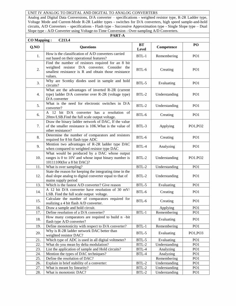
UNIT IV ANALOG TO DIGITAL AND DIGITAL TO ANALOG CONVERTERS
Analog and Digital Data Conversions, D/A converter – specifications - weighted resistor type, R-2R Ladder type,
Voltage Mode and Current-Mode R-2R Ladder types - switches for D/A converters, high speed sample-and-hold
circuits, A/D Converters – specifications - Flash type - Successive Approximation type - Single Slope type – Dual
Slope type - A/D Converter using Voltage-to-Time Conversion - Over-sampling A/D Converters.
PART-A
CO Mapping : C213.4
Q.NO Questions BT
Level Competence
PO
1. How is the classification of A/D converters carried
out based on their operational features? BTL-1 Remembering PO1
2.
Find the number of resistors required for an 8 bit
weighted resistor D/A converter. Consider the
smallest resistance is R and obtain those resistance
values.
BTL-6 Creating PO1
3. Why are Scottky diodes used in sample and hold
circuits? BTL-5 Evaluating PO1
4.
What are the advantages of inverted R-2R (current
type) ladder D/A converter over R-2R (voltage type)
D/A converter
BTL-2 Understanding PO1
5. What is the need for electronic switches in D/A
converter? BTL-2 Understanding PO1
6. A 12 bit D/A converter has a resolution of
20mv/LSB.Find the full scale output voltage. BTL-6 Creating PO1
7.
Draw the binary ladder network of DAC, If the value
of the smaller resistance is 10K.What is the value of
other resistance?
BTL-3 Applying PO1,PO2
8. Determine the number of comparators and resistors
required for 8 bit flash type ADC BTL-6 Creating PO1
9. Mention two advantages of R-2R ladder type DAC
when compared to weighted resistor type DAC BTL-4 Analyzing PO1
10.
What would be produced by a DAC whose output
ranges is 0 to 10V and whose input binary number is
10111100(for a 8 bit DAC)?
BTL-2 Understanding PO1.PO2
11. What is over sampling? BTL-2 Understanding PO1
12.
State the reason for keeping the integrating time in the
dual slope analog to digital converter equal to that of
mains supply period
BTL-2 Understanding PO1
13. Which is the fastest A/D converter? Give reason BTL-5 Evaluating PO1
14. A 12 bit D/A converter have resolution of 30 mV/
LSB. Find the full scale output voltage. BTL-6 Creating PO1
15. Calculate the number of comparators required for
realizing a 4 bit flash A/D converter. BTL-6 Creating PO1
16. Draw a sample and hold circuit. Applying PO1
17. Define resolution of a D/A converter? BTL-1 Remembering PO1
18. How many comparators are required to build n –bit
flash type A/D converter? Evaluating PO1
19. Define monotonicity with respect to D/A converter? BTL-1 Remembering PO1
20. Why is R-2R ladder network DAC better than
weighted resistor DAC? BTL-5 Evaluating PO1,PO3
21. Which type of ADC is used in all digital voltmeter? BTL-5 Evaluating PO1
22. What do you mean by delta modulation? BTL-2 Understanding PO1
23. List the application of sample and Hold circuits? BTL-4 Analyzing PO1
24. Mention the types of DAC techniques? BTL-4 Analyzing PO1
25. Define the resolution of DAC? Remembering PO1
26. Explain in brief stability of a converter: BTL-2 Understanding PO1
27. What is meant by linearity? BTL-2 Understanding PO1
28. What is monotonic DAC? BTL-2 Understanding PO1
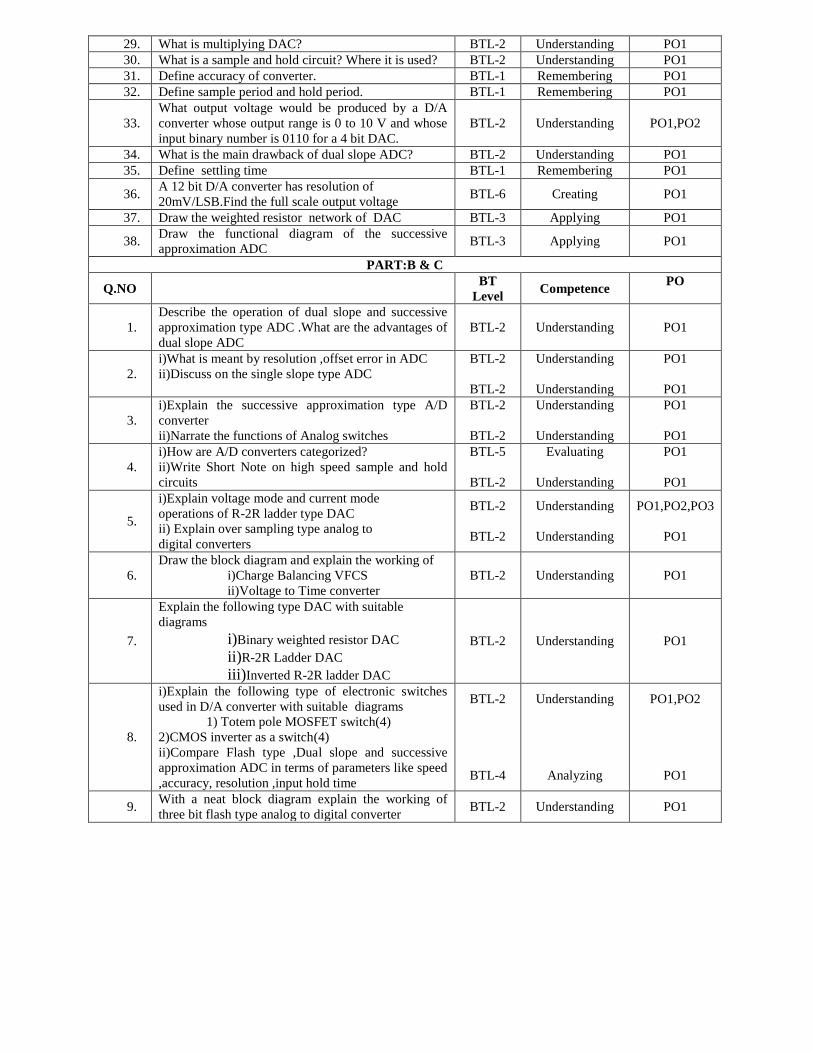
29. What is multiplying DAC? BTL-2 Understanding PO1
30. What is a sample and hold circuit? Where it is used? BTL-2 Understanding PO1
31. Define accuracy of converter. BTL-1 Remembering PO1
32. Define sample period and hold period. BTL-1 Remembering PO1
33.
What output voltage would be produced by a D/A
converter whose output range is 0 to 10 V and whose
input binary number is 0110 for a 4 bit DAC.
BTL-2 Understanding PO1,PO2
34. What is the main drawback of dual slope ADC? BTL-2 Understanding PO1
35. Define settling time BTL-1 Remembering PO1
36. A 12 bit D/A converter has resolution of
20mV/LSB.Find the full scale output voltage BTL-6 Creating PO1
37. Draw the weighted resistor network of DAC BTL-3 Applying PO1
38. Draw the functional diagram of the successive
approximation ADC BTL-3 Applying PO1
PART:B & C
Q.NO BT
Level Competence
PO
1.
Describe the operation of dual slope and successive
approximation type ADC .What are the advantages of
dual slope ADC
BTL-2 Understanding PO1
2.
i)What is meant by resolution ,offset error in ADC
ii)Discuss on the single slope type ADC
BTL-2
BTL-2
Understanding
Understanding
PO1
PO1
3.
i)Explain the successive approximation type A/D
converter
ii)Narrate the functions of Analog switches
BTL-2
BTL-2
Understanding
Understanding
PO1
PO1
4.
i)How are A/D converters categorized?
ii)Write Short Note on high speed sample and hold
circuits
BTL-5
BTL-2
Evaluating
Understanding
PO1
PO1
5.
i)Explain voltage mode and current mode
operations of R-2R ladder type DAC
ii) Explain over sampling type analog to
digital converters
BTL-2
BTL-2
Understanding
Understanding
PO1,PO2,PO3
PO1
6.
Draw the block diagram and explain the working of
i)Charge Balancing VFCS
ii)Voltage to Time converter
BTL-2 Understanding PO1
7.
Explain the following type DAC with suitable
diagrams
i)Binary weighted resistor DAC
ii)R-2R Ladder DAC
iii)Inverted R-2R ladder DAC
BTL-2 Understanding PO1
8.
i)Explain the following type of electronic switches
used in D/A converter with suitable diagrams
1) Totem pole MOSFET switch(4)
2)CMOS inverter as a switch(4)
ii)Compare Flash type ,Dual slope and successive
approximation ADC in terms of parameters like speed
,accuracy, resolution ,input hold time
BTL-2
BTL-4
Understanding
Analyzing
PO1,PO2
PO1
9. With a neat block diagram explain the working of
three bit flash type analog to digital converter BTL-2 Understanding PO1
UNIT V WAVEFORM GENERATORS AND SPECIAL FUNCTION ICS
Sine-wave generators, Multivibrators and Triangular wave generator, Saw-tooth wave generator, ICL8038 function
generator, Timer IC 555, IC Voltage regulators – Three terminal fixed and adjustable voltage regulators - IC 723
general purpose regulator - Monolithic switching regulator, Switched capacitor filter IC MF10, Frequency to
Voltage and Voltage to Frequency converters, Audio Power amplifier, Video Amplifier, Isolation Amplifier, Opto-
couplers and fibre optic IC.
PART-A
CO Mapping : C213.5
Q.NO Questions BT
Level Competence
PO
1. Define current transfer ratio of an opto coupler BTL-1 Remembering PO1
2. Draw a fixed voltage regulator circuit and state its
operation BTL-1 Remembering PO1
3. What is a voltage regulator? BTL-2 Understanding PO1
4. Distinguish the principle of linear regulator and a
switched mode power supply. BTL-4 Analyzing PO1
5. Draw the block schematic of IC 555 timer. BTL-1 Remembering PO1,PO2
6. Draw the internal circuit for audio power amplifier BTL-1 Remembering PO1
7. What is the function of a voltage regulator? Name
few IC voltage regulators. BTL-1 Remembering PO1
8. Give the classification of voltage regulators: BTL-2 Understanding PO1
9. Mention some applications of 555 timer: BTL-4 Analyzing PO1
10. List the applications of 555 timer in monostable mode
of operation: BTL-1 Remembering PO1,PO2,PO3
11. List the applications of 555 timer in Astable mode of
operation: BTL-1 Remembering PO1,PO2,PO3
12. What is a linear voltage regulator? BTL-2 Understanding PO1
13. What is a switching regulator? BTL-2 Understanding PO1
14. What is the purpose of having input and output
capacitors in three terminal IC regulators? BTL-2 Understanding PO1
15. Define line regulation. BTL-1 Remembering PO1
16. Define load regulation BTL-1 Remembering PO1
17. What is meant by current limiting? BTL-2 Understanding PO1
18. Give the drawbacks of linear regulators: BTL-3 Applying PO1
19. What is the advantage of switching regulators? BTL-2 Understanding PO1
20. What is an opto-coupler IC? Give examples. BTL-2 Understanding PO1
21. Mention the advantages of opto-couplers: Analyzing PO1
22. What is an isolation amplifier? BTL-2 Understanding PO1
23. What is the need for a tuned amplifier? BTL-2 Understanding PO1
24. Give the classification of tuned amplifier BTL-2 Understanding PO1
25. State the two conditions for oscillation. BTL-2 Understanding PO1
26. Draw the functional block diagram of 723 regulator. BTL-3 Applying PO1
27. Why is the monostable multivibrator circuit called
time delay circuit and gating circuit? BTL-2 Understanding PO1,PO2
28. Why there is no phase shift provided in the feedback
network in Wein-Bridge oscillator? BTL-2 Understanding PO1
29. Give the formula for period of oscillations in an op-
amp astable circuit. BTL-3 Applying PO1
30. Define duty cycle for a periodic pulse waveform. BTL-1 Remembering PO1
31. What is meant by thermal shutdown applied to
voltage regulators? BTL-2 Understanding PO1
32. What are the three waveforms generated by ICL8038? BTL-2 Understanding PO1
33. List the characteristics of optocoupler BTL-1 Remembering PO1
34. Mention two applications of frequency to voltage
converter BTL-4 Analyzing PO1
35. What is the advantage of switching regulators? BTL-2 Understanding PO1
PART:B & C
Q.NO BT Competence PO
Level
1. i)With neat diagram explain the operation of an
astable and monostablemultivibrators
ii)Draw the functional diagram and connection
diagram of a low voltage regulator and explain
BTL-2
BTL-3
Understanding
Applying
PO1,PO12
PO1
2. Answer any two of the following1) Switched
capacitor filters
2)Audio power amplifier
3)Opto coupler
BTL-2 Understanding PO1
3. With neat diagram explain IC723 general purpose
voltage regulator BTL-2 Understanding PO1
4. Explain Sawtooth waveform generator and LM
380Audio amplifier in detail BTL-2 Understanding PO1
5. Describe the working of a astable
multivibrator using 555 timer BTL-2 Understanding PO1
6. Explain in detail Voltage to frequency and frequency
to voltage converter BTL-2 Understanding PO1
7. i)Design a phase shift oscillate at 100Hz
ii)Describe monostablemultivibrator with necessary
diagrams and derive for ON time and recovery time
BTL-6
BTL-2
Creating
Understanding
PO1,PO2
PO1
8. i)Briefly describe about monolithic switching
regulators
ii)Draw the schematic of ICL 8038 function generator
and discuss its features
BTL-2
BTL-3
Understanding
Applying
PO1
PO2
9. Describe the working of a Astablemultivibrator using
op-amp BTL-2 Understanding PO1
10. Describe the working of a monostablemultivibrator
using 555 timer BTL-2 Understanding PO1
11. Explain Video amplifier and opto-couplers BTL-2 Understanding PO1
UNIT I- BASICS OF OPERATIONAL AMPLIFIERS
Current mirror and current sources, Current sources as active loads, Voltage sources, Voltage References, BJT
Differential amplifier with active loads, Basic information about op-amps – Ideal Operational Amplifier - General
operational amplifier stages -and internal circuit diagrams of IC 741, DC and AC performance characteristics, slew
rate, Open and closed loop configurations.
PART-A
1.Draw the dc transfer characteristics of a BJT differential amplifier and define differential mode input voltage
[Nov/Dec 2017]
2. Write down the characteristics of ideal operational amplifier? [April/May 2017][April/May 16]
Open loop voltage gain, (AOL) = ∞
Input impedance (Ri) = ∞
Output impedance (Ro) = 0
Bandwidth (BW) = ∞
Zero offset Vo = 0, when V1 = V2 = 0
3.Why is the current mirror circuit used in differential amplifier stages? [April/May 2017]
The current mirror is a special case of constant current bias and the current mirror bias requires of
constant current bias and therefore can be used to set up currents in differential amplifier stages
4. Differentiate the ideal and practical characteristics of an op-amp[MAY/JUNE 2016]
Characteristics Ideal Practical
Open loop voltage gain ∞ High
5. Input impedance (Ri) 6. ∞ 7. High
Output impedance (Ro) 0 Low
Bandwidth (BW) ∞ High
Zero offset Vo = 0, when V1 = V2 = 0 Non zero
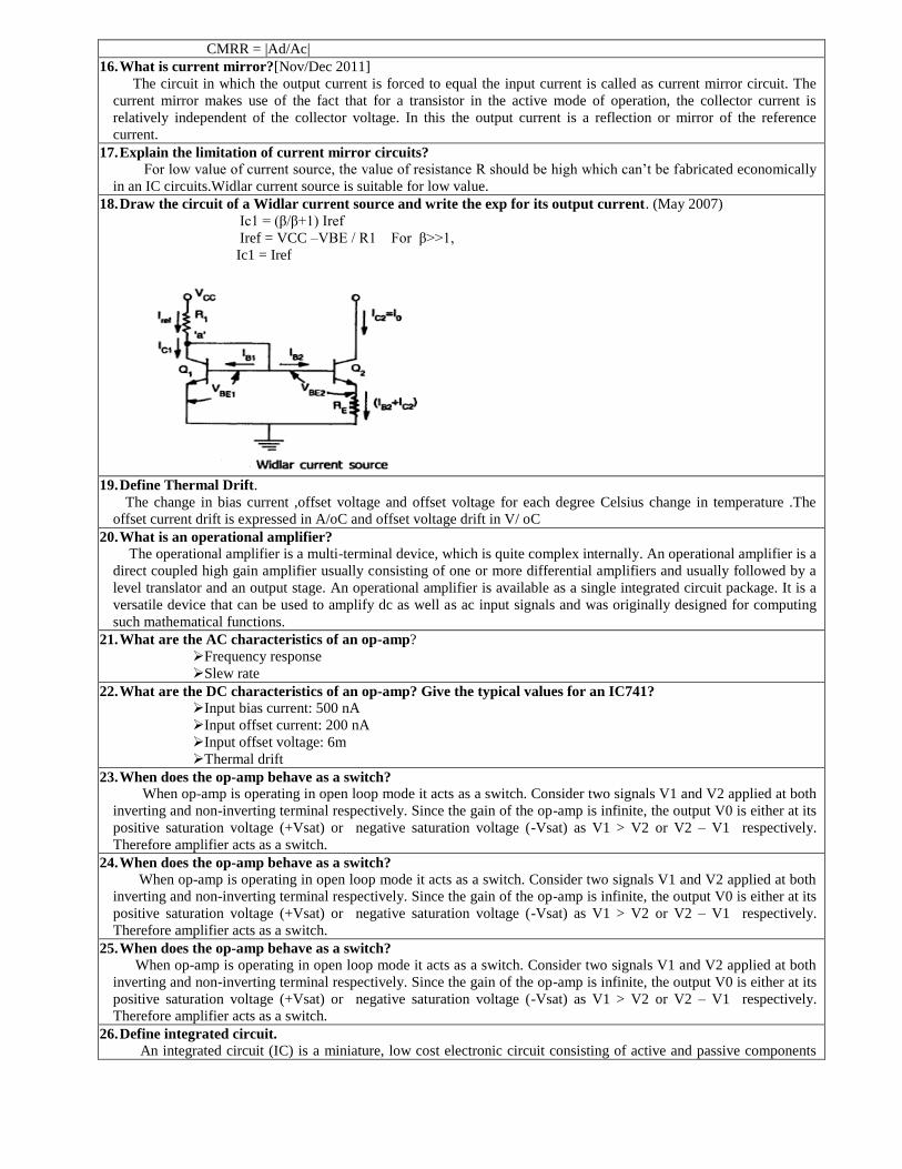
8.Draw the circuit diagram of a symmetrical emitter coupled differential amplifier. [Nov/Dec 2016]
9.Draw the Internal Block diagram of Op – Amp (IC 741) [Nov/Dec 2016]
10. An operational amplifier has a slew rate of 4v/µs .Determine the maximum frequency of operation to produce
distortion less output swing of 12V [APRIL/MAY 16]
Frequency f = slewrate(SR) / 2ПVm
= 4 / (2* П*12)
= 0.013 Hz
11. What is the cause for slew rate and how it can be made faster? [APRIL/MAY 2015]
There is a capacitor within or outside an op-amp to prevent oscillation. It is this capacitor which prevents the output
voltage from responding immediately to a fast changing input .The slew rate can be made faster by having a higher
current or a small compensating capacitor
12. Define input bias current and input offset current of an operational amplifier[Nov/Dec 2015]
Input bias current is the average value of the base current entering in to the i/p terminals of an opamp.Its typical
value is 500nA
Input offset current is the algebraic difference between the current into the inverting and non-inverting terminals is
referred to as input offset current Iio. Mathematically it is represented as
Iio = |IB+- IB-|
Where IB+ is the current into the non-inverting input terminals.
IB- is the current into the inverting input terminals.
13. A differential amplifier has a differential voltage gain of 2000 and a common mode gain of 0.2.Determine the
CMRR in dB [April/May 2015]
Given common mode gain Acm=0.2
Difference mode gain Adm=2000
CMRR= Adm/ Acm= 2000/0.2 =10000=10log10000=80dB
14. Define Slew rate and what causes slew rate?[April/May 2015]
The slew rate of an op amp or any amplifier circuit is the rate of change in the output voltage caused by a step
change on the input.
There is usually a capacitor within or outside an op-amp to prevent oscillation. It is this capacitor which prevents
the output voltage from responding immediately to a fast changing input
15. Define CMRR of an operational amplifier? [May/June 2013]
The common mode rejection ratio (CMRR) can be defined as the ratio of differential gain to common mode gain.
CMRR = |Ad/Ac|
16. What is current mirror?[Nov/Dec 2011]
The circuit in which the output current is forced to equal the input current is called as current mirror circuit. The
current mirror makes use of the fact that for a transistor in the active mode of operation, the collector current is
relatively independent of the collector voltage. In this the output current is a reflection or mirror of the reference
current.
17. Explain the limitation of current mirror circuits?
For low value of current source, the value of resistance R should be high which can’t be fabricated economically
in an IC circuits.Widlar current source is suitable for low value.
18. Draw the circuit of a Widlar current source and write the exp for its output current. (May 2007)
Ic1 = (β/β+1) Iref
Iref = VCC –VBE / R1 For β>>1,
Ic1 = Iref
19. Define Thermal Drift.
The change in bias current ,offset voltage and offset voltage for each degree Celsius change in temperature .The
offset current drift is expressed in A/oC and offset voltage drift in V/ oC
20. What is an operational amplifier?
The operational amplifier is a multi-terminal device, which is quite complex internally. An operational amplifier is a
direct coupled high gain amplifier usually consisting of one or more differential amplifiers and usually followed by a
level translator and an output stage. An operational amplifier is available as a single integrated circuit package. It is a
versatile device that can be used to amplify dc as well as ac input signals and was originally designed for computing
such mathematical functions.
21. What are the AC characteristics of an op-amp?
Frequency response
Slew rate
22. What are the DC characteristics of an op-amp? Give the typical values for an IC741?
Input bias current: 500 nA
Input offset current: 200 nA
Input offset voltage: 6m
Thermal drift
23. When does the op-amp behave as a switch?
When op-amp is operating in open loop mode it acts as a switch. Consider two signals V1 and V2 applied at both
inverting and non-inverting terminal respectively. Since the gain of the op-amp is infinite, the output V0 is either at its
positive saturation voltage (+Vsat) or negative saturation voltage (-Vsat) as V1 > V2 or V2 – V1 respectively.
Therefore amplifier acts as a switch.
24. When does the op-amp behave as a switch?
When op-amp is operating in open loop mode it acts as a switch. Consider two signals V1 and V2 applied at both
inverting and non-inverting terminal respectively. Since the gain of the op-amp is infinite, the output V0 is either at its
positive saturation voltage (+Vsat) or negative saturation voltage (-Vsat) as V1 > V2 or V2 – V1 respectively.
Therefore amplifier acts as a switch.
25. When does the op-amp behave as a switch?
When op-amp is operating in open loop mode it acts as a switch. Consider two signals V1 and V2 applied at both
inverting and non-inverting terminal respectively. Since the gain of the op-amp is infinite, the output V0 is either at its
positive saturation voltage (+Vsat) or negative saturation voltage (-Vsat) as V1 > V2 or V2 – V1 respectively.
Therefore amplifier acts as a switch.
26. Define integrated circuit.
An integrated circuit (IC) is a miniature, low cost electronic circuit consisting of active and passive components
fabricated together on a single crystal of silicon. The active components are transistors and diodes and passive
components are resistors inductors and capacitors
27. What are the advantages of integrated circuits over discrete components?
Miniaturization and hence increased equipment density.
Cost reduction due to batch processing.
Increased system reliability due to the elimination of soldered joints.
Improved functional performance.
Matched devices.
Increased operating speeds.
Reduction in power consumption
28. What are the disadvantages of integrated circuits
Inductors can’t be fabricated
IC’s function at fairly low voltage
They can handle only limited amount of power.
It can’t withstand for rough handling and excessive heat
29. What is meant by monolithic IC
A monolithic integrated circuit (IC) is an electronic circuit that is built on a single semiconductor base material or
single chip
30. What are the two requirements to be met for a good current source?
A good current source must meet two requirements:
Output current IO should not depend on β;
Output Resistance (RO) of the current source should be very high;
31. List the various methods of realizing high input resistance in a differential amplifier.
The various methods of realizing high input resistance in a differential amplifier circuits are
Use of Darlington pair
Use of FET
Use of swamping resistors
32. Mention two advantages of active load over passive load in an operational amplifier[NOV/DEC 2015]
Larger gain
Larger Bandwidth
33. What is active load? Where it is used and why?
In circuit design, an active load is a circuit component made up of active devices, such as transistors, intended to
present a high small-signal impedance yet not requiring a large DC voltage drop, as would occur if a large resistor
were used instead. Such large AC load impedances may be desirable, for example, to increase the AC gain of some
types of amplifier.
Most commonly the active load is the output part of a current mirror and is represented in an idealized manner as
a current source. Usually, it is only a constant-current resistor that is a part of the whole current source including a
constant voltage source as well
34. Define supply voltage rejection ratio (SVRR)
The change in OPAMP’s input offset voltage due to variations in supply voltage is called the supply voltage
rejection ratio. It is also called Power Supply Rejection Ratio (PSRR) or Power Supply Sensitivity (PSS)
35. Define input offset voltage
The input offset voltage is a parameter defining the differential DC voltage required between the inputs of
an amplifier, especially an operational amplifier (op-amp), to make the output zero
36. Define Frequency Response
Frequency response is the quantitative measure of the output spectrum of a system or device in response to a
stimulus, and is used to characterize the dynamics of the system. It is a measure of magnitude and phase of the output
as a function of frequency, in comparison to the input
37. Define unity gain bandwidth of a Op-Amp
The GBWP (Gain Band Width Product) of an operational amplifier is 1 MHz, it means that the gain of the device
falls to unity at 1 MHz. Hence, when the device is wired for unity gain, it will work up to 1 MHz
(GBWP = gain × bandwidth, therefore if BW = 1 MHz, then gain = 1) without excessively distorting the signal.
PART B& C
1.i) With a help of a block diagram ,explain the various stages present in an operational
amplifier[Nov/Dec 2017]
[Ref .Roy Choudhry, ShailB.Jain, “Linear Integrated Circuits (Fourth Edition)”, Page 108]
ii) Draw the transfer characteristics of an operational amplifier and explain the linear and non-linear
operation[Nov/Dec 2017]
[Ref .Roy Choudhry, ShailB.Jain, “Linear Integrated Circuits (Fourth Edition)”, Page 108]
2.i) What is the input and output voltage and current offsets? How are they compensated?
[April/May 2017]
[Ref .Roy Choudhry, ShailB.Jain, “Linear Integrated Circuits (Fourth Edition)”, Page 108]
ii) With neat diagram derive the AC performance close loop characteristics of Op-Amp to discuss on
the circuit Bandwidth, Frequency response and slew rate[April/May 2017]
[Ref .Roy Choudhry, ShailB.Jain, “Linear Integrated Circuits (Fourth Edition)”, Page 111]
3.i) With a schematic diagram,explain the effect of RE on CMRR in differential amplifier[April/May 16]
[Ref .Roy Choudhry, Shail B.Jain, “Linear Integrated Circuits (Second Edition)”, Page 63].
ii) Discuss about the methods to improve CMRR[April/May 16]
4.i) With simple schematic of differential amplifier explain the function of Operational Amplifier
[April/May 2015]
[Ref .Roy Choudhry, Shail B.Jain, “Linear Integrated Circuits (Second Edition)”, Page 63]
ii) Briefly Explain about constant current source [April/May2015](8)
[Ref .Roy Choudhry, Shail B.Jain, “Linear Integrated Circuits (Second Edition)”, Page 73]
5.i) Briefly explain the techniques used for frequency compensation[April/May2015] (12)
[Ref .Roy Choudhry, Shail B.Jain, “Linear Integrated Circuits (Second Edition)”, Page 135]
ii) How do the open loop gain and the closed loop gain of an op-amp differ? [April/May2015] (4)
[Ref .Roy Choudhry, Shail B.Jain, “Linear Integrated Circuits (Second Edition)”, Page 225]
6.With a neat diagram Explain the input side of the internal circuit diagram of IC741[Nov/dec 15]
[Ref .Roy Choudhry, Shail B.Jain, “Linear Integrated Circuits (Second Edition)”, Page 96]
7.What is the need for frequency compensation in an OPAMP? With a suitable illustration, explain the pole-zero
frequency compensation technique. [Nov/dec 15][April/May 2017]
[Ref .Roy Choudhry, Shail B.Jain, “Linear Integrated Circuits (Second Edition)”, Page 135]
8.Draw the circuit of basic current mirror and explain its operation. Also discuss about how current ratio can be
improved in the basic current mirror.Sketch the improved circuit and explain[Nov/dec 12]
[Ref .Roy Choudhry, Shail B.Jain, “Linear Integrated Circuits (Second Edition)”, Page 73]
9.(i) Define and explain slew rate. What is full power bandwidth? Also explain the method adopted to
improve slew rate[Nov/dec 12]
[Ref .Roy Choudhry, Shail B.Jain, “Linear Integrated Circuits (Second Edition)”, Page 140]
(ii) Define output off set voltage. Explain methods to nullify offset voltage[Nov/dec 12]
[Ref .Roy Choudhry, Shail B.Jain, “Linear Integrated Circuits (Second Edition)”, Page 123]
10.Explain in detail wilson current source and widlar current source and derive necessary equations
[Ref .Roy Choudhry, Shail B.Jain, “Linear Integrated Circuits (Second Edition)”, Page 75]
UNIT II -APPLICATIONS OF OPERATIONAL AMPLIFIERS
Sign Changer, Scale Changer, Phase Shift Circuits, Voltage Follower, V-to-I and I-to-V converters, adder, subtractor,
Instrumentation amplifier, Integrator, Differentiator, Logarithmic amplifier, Antilogarithmic amplifier, Comparators,
Schmitt trigger, Precision rectifier, peak detector, clipper and clamper, Low-pass, high-pass and band-pass
Butterworth filters.
PART-A
1.State the limitations of an ideal integrator.[Nov/Dec 2017]
Bandwidth is very small and used for only small range of input frequencies.
For dc input (f = 0), reactance of capacitance, Xc is infinite. Because of this op-amp goes into open loop
configuration. In open loop configuration the gain is infinite and hence the small input offset voltages
are also amplified and appears at output as error
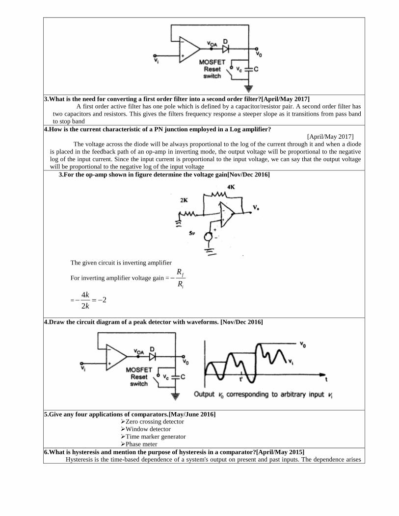
2.How will you realize a peak detector using a precision rectifier?[Nov/Dec 2017]
3.What is the need for converting a first order filter into a second order filter?[April/May 2017]
A first order active filter has one pole which is defined by a capacitor/resistor pair. A second order filter has
two capacitors and resistors. This gives the filters frequency response a steeper slope as it transitions from pass band
to stop band
4.How is the current characteristic of a PN junction employed in a Log amplifier?
[April/May 2017]
The voltage across the diode will be always proportional to the log of the current through it and when a diode
is placed in the feedback path of an op-amp in inverting mode, the output voltage will be proportional to the negative
log of the input current. Since the input current is proportional to the input voltage, we can say that the output voltage
will be proportional to the negative log of the input voltage
3.For the op-amp shown in figure determine the voltage gain[Nov/Dec 2016]
The given circuit is inverting amplifier
For inverting amplifier voltage gain =f
i
R
R
=4
22
k
k
4.Draw the circuit diagram of a peak detector with waveforms. [Nov/Dec 2016]
5.Give any four applications of comparators.[May/June 2016]
Zero crossing detector
Window detector
Time marker generator
Phase meter
6.What is hysteresis and mention the purpose of hysteresis in a comparator?[April/May 2015]
Hysteresis is the time-based dependence of a system's output on present and past inputs. The dependence arises
because the history affects the value of an internal state. To predict its future outputs, either its internal state or its
history must be known.
In comparator hysteresis has the effect of separating the up-going and down-going switching points so that, once
a transition has started, the input must undergo a significant reversal before the reverse transition can occur.
7.What is the difference between normal rectifier and precision rectifier?[April/May 2015]
A simple rectifier circuit uses a diode. The input voltage has to exceed the turn-on voltage (0.6V for ordinary
Si diode) before rectification is achieved.
A precision rectifier is an active circuit using an opamp and a diode in the feedback loop. This overcomes the
turn-on "knee" voltage
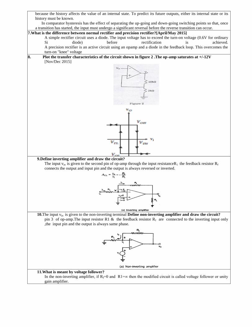
8. Plot the transfer characteristics of the circuit shown in figure 2 .The op-amp saturates at +/-12V
[Nov/Dec 2015]
9.Define inverting amplifier and draw the circuit?
The input vin is given to the second pin of op-amp through the input resistanceR1 the feedback resistor Rf
connects the output and input pin and the output is always reversed or inverted.
10.The input vin is given to the non-inverting terminal Define non-inverting amplifier and draw the circuit?
pin 3 of op-amp.The input resistor R1 & the feedback resistor Rf are connected to the inverting input only
,the input pin and the output is always same phase.
11.What is meant by voltage follower?
In the non-inverting amplifier, if Rf=0 and R1=∞ then the modified circuit is called voltage follower or unity
gain amplifier.
12.Draw the circuit diagram of an op-amp integrator. Mention its applications.
Application:
1. It is generally used in analog computer and analog to digital converter.
2. It also used in wave shaping circuits
13.Draw the circuit diagram of an op-amp differential amplifier. Mention its o/p equation. [NOV/DEC2016]
14.For the op-amp shown in figure, determine the voltage gain.
10K
+
-
3
26
74
2K
5V
Vo
Vo / Vin = 1+Rf / R1
= 1+ 10K / 2K
= 6
15.Explain the voltage to current convertor
Voltage to current convertor converts an input signal voltage to a proportional output current
According to the connection of load there are two types of voltage to current convertor
1. Floating type
2. Grounded type
16.Draw the circuit of a voltage follower using op-amp and prove that its gain is exactly equal to unity.
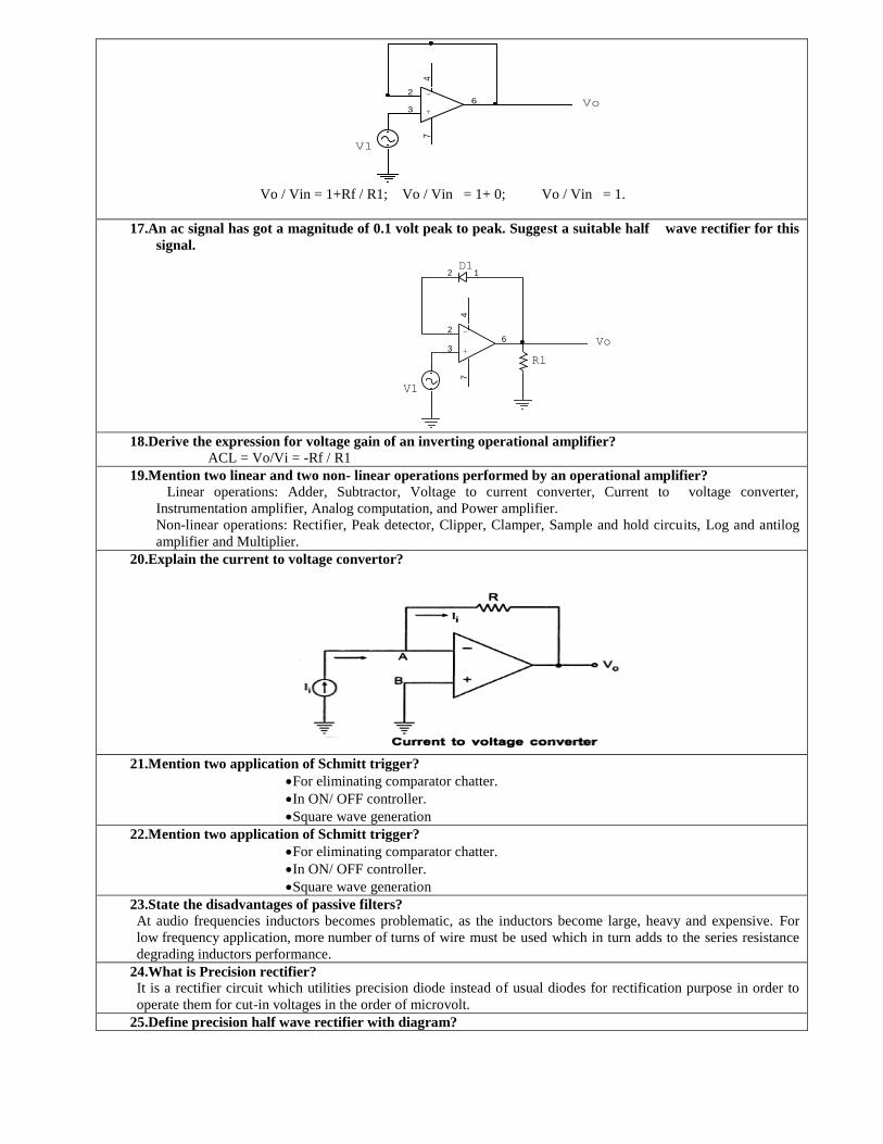
+
-
3
26
74
Vo
V1
Vo / Vin = 1+Rf / R1; Vo / Vin = 1+ 0; Vo / Vin = 1.
17.An ac signal has got a magnitude of 0.1 volt peak to peak. Suggest a suitable half wave rectifier for this
signal.
D1
+
-
3
26
74
Vo
Rl
V1
12
18.Derive the expression for voltage gain of an inverting operational amplifier?
ACL = Vo/Vi = -Rf / R1
19.Mention two linear and two non- linear operations performed by an operational amplifier?
Linear operations: Adder, Subtractor, Voltage to current converter, Current to voltage converter,
Instrumentation amplifier, Analog computation, and Power amplifier.
Non-linear operations: Rectifier, Peak detector, Clipper, Clamper, Sample and hold circuits, Log and antilog
amplifier and Multiplier.
20.Explain the current to voltage convertor?
21.Mention two application of Schmitt trigger?
For eliminating comparator chatter.
In ON/ OFF controller.
Square wave generation
22.Mention two application of Schmitt trigger?
For eliminating comparator chatter.
In ON/ OFF controller.
Square wave generation
23.State the disadvantages of passive filters?
At audio frequencies inductors becomes problematic, as the inductors become large, heavy and expensive. For
low frequency application, more number of turns of wire must be used which in turn adds to the series resistance
degrading inductors performance.
24.What is Precision rectifier?
It is a rectifier circuit which utilities precision diode instead of usual diodes for rectification purpose in order to
operate them for cut-in voltages in the order of microvolt.
25.Define precision half wave rectifier with diagram?
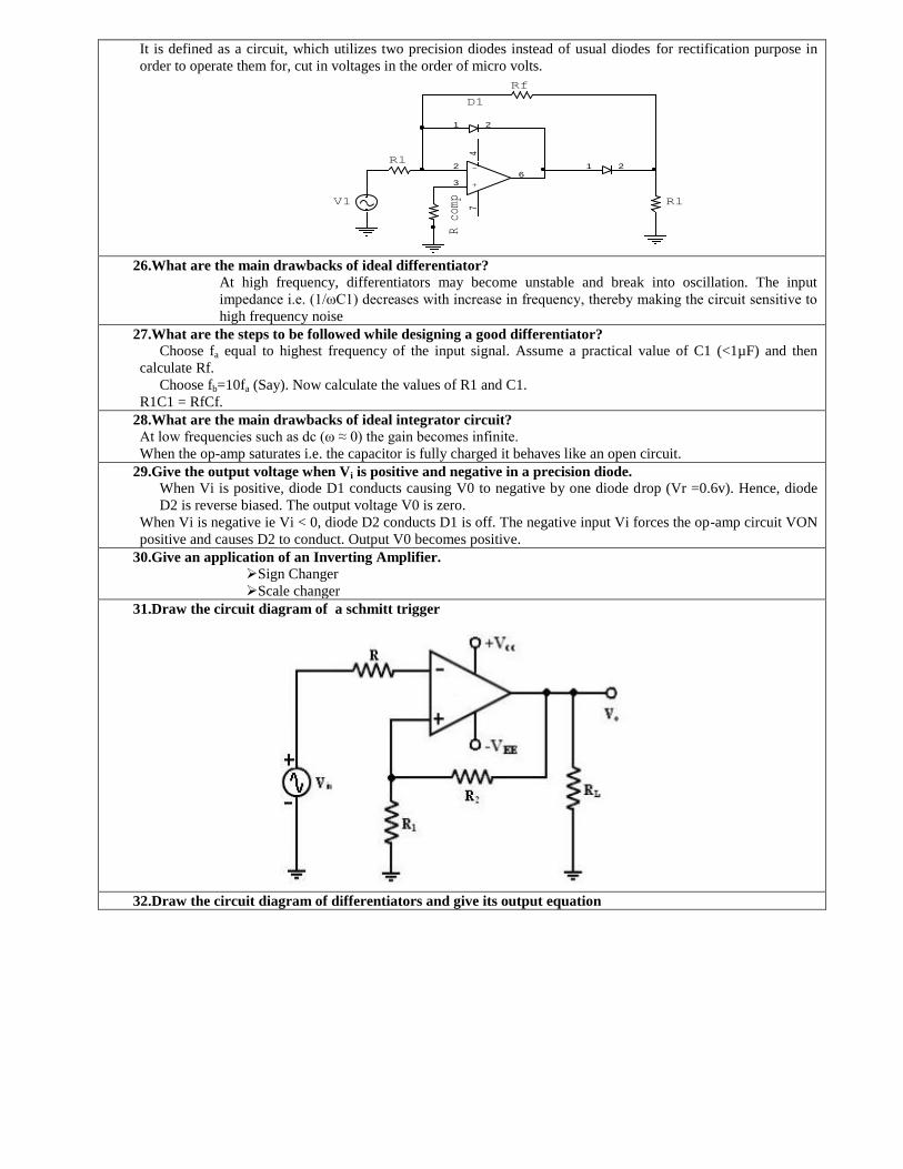
It is defined as a circuit, which utilizes two precision diodes instead of usual diodes for rectification purpose in
order to operate them for, cut in voltages in the order of micro volts.
1 2
V1
Rf
D1
+
-
3
26
74
Rl
Rl
1 2
R comp
26.What are the main drawbacks of ideal differentiator?
At high frequency, differentiators may become unstable and break into oscillation. The input
impedance i.e. (1/ωC1) decreases with increase in frequency, thereby making the circuit sensitive to
high frequency noise
27.What are the steps to be followed while designing a good differentiator?
Choose fa equal to highest frequency of the input signal. Assume a practical value of C1 (<1µF) and then
calculate Rf.
Choose fb=10fa (Say). Now calculate the values of R1 and C1.
R1C1 = RfCf.
28.What are the main drawbacks of ideal integrator circuit?
At low frequencies such as dc (ω ≈ 0) the gain becomes infinite.
When the op-amp saturates i.e. the capacitor is fully charged it behaves like an open circuit.
29.Give the output voltage when Vi is positive and negative in a precision diode.
When Vi is positive, diode D1 conducts causing V0 to negative by one diode drop (Vr =0.6v). Hence, diode
D2 is reverse biased. The output voltage V0 is zero.
When Vi is negative ie Vi < 0, diode D2 conducts D1 is off. The negative input Vi forces the op-amp circuit VON
positive and causes D2 to conduct. Output V0 becomes positive.
30.Give an application of an Inverting Amplifier.
Sign Changer
Scale changer
31.Draw the circuit diagram of a schmitt trigger
32.Draw the circuit diagram of differentiators and give its output equation
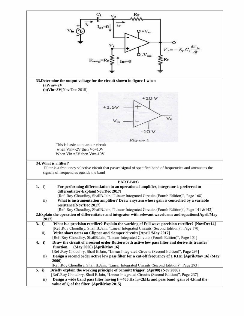
33.Determine the output voltage for the circuit shown in figure 1 when
(a)Vin=-2V
(b)Vin=3V[Nov/Dec 2015]
This is basic comparator circuit
when Vin=-2V then Vo=10V
When Vin =3V then Vo=-10V
34. What is a filter?
Filter is a frequency selective circuit that passes signal of specified band of frequencies and attenuates the
signals of frequencies outside the band
PART-B&C
1. i) For performing differentiation in an operational amplifier, integrator is preferred to
differentiator-Explain[Nov/Dec 2017]
[Ref .Roy Choudhry, ShailB.Jain, “Linear Integrated Circuits (Fourth Edition)”, Page 168]
ii) What is instrumentation amplifier? Draw a system whose gain is controlled by a variable
resistance[Nov/Dec 2017]
[Ref .Roy Choudhry, ShailB.Jain, “Linear Integrated Circuits (Fourth Edition)”, Page 141 &142]
2.Explain the operation of differentiator and integrator with relevant waveforms and equations[April/May
2017]
3. i) What is a precision rectifier? Explain the working of Full wave precision rectifier? [Nov/Dec14]
[Ref .Roy Choudhry, Shail B.Jain, “Linear Integrated Circuits (Second Edition)”, Page 170]
ii) Write short notes on Clipper and clamper circuits [April /May 2017]
[Ref .Roy Choudhry, ShailB.Jain, “Linear Integrated Circuits (Fourth Edition)”, Page 151]
4. i) Draw the circuit of a second order Butterworth active low pass filter and derive its transfer
function. (May 2006) [April/May 16]
[Ref .Roy Choudhry, Shail B.Jain, “Linear Integrated Circuits (Second Edition)”, Page 293]
ii) Design a second order active low pass filter for a cut-off frequency of 1 KHz. [April/May 16] (May
2006)
[Ref .Roy Choudhry, Shail B.Jain, “Linear Integrated Circuits (Second Edition)”, Page 293]
5. i) Briefly explain the working principle of Schmitt trigger. (Apr08) (Nov 2006)
[Ref .Roy Choudhry, Shail B.Jain, “Linear Integrated Circuits (Second Edition)”, Page 237]
ii) Design a wide band pass filter having fL=400 Hz fH=2kHz and pass band gain of 4.Find the
value of Q of the filter (April/May 2015)
[Ref .Roy Choudhry, Shail B.Jain, “Linear Integrated Circuits (Second Edition)”, Page 306]
6.With a circuit diagram discuss the following applications of op-amp. (Nov 2006)
c. Voltage to current converter.
d. Precision rectifier.
[Ref .Roy Choudhry, Shail B.Jain, “Linear Integrated Circuits (Second Edition)”, Page 166 &169]
7.Explain the working of 3 op-amp Instrumentation amplifier? [Nov/Dec 14] [April/May 16]
[Ref .Roy Choudhry, Shail B.Jain, “Linear Integrated Circuits (Second Edition)”, Page 161]
8.Explain the working of Log amplifier and antilog amplifier? [May/June 14]
[Ref .Roy Choudhry, Shail B.Jain, “Linear Integrated Circuits (Second Edition)”, Page 178]
9.i) Explain the operation of current to voltage converter
[Ref .Roy Choudhry, Shail B.Jain, “Linear Integrated Circuits (Fourth Edition)”, Page 147]
ii) Differentiate between low pass ,high pass ,band pass and band reject filter.Sketch the frequency
plot
[Ref .Roy Choudhry, ShailB.Jain, “Linear Integrated Circuits (Fourth Edition)”, Page 263]
UNIT III-ANALOG MULTIPLIER AND PLL
Analog Multiplier using Emitter Coupled Transistor Pair - Gilbert Multiplier cell – Variable transconductance
technique, analog multiplier ICs and their applications, Operation of the basic PLL, Closed loop analysis, Voltage
controlled oscillator, Monolithic PLL IC 565, application of PLL for AM detection, FM detection, FSK modulation
and demodulation and Frequency synthesizing
PART-A
1.Define capture range of a PLL? [Nov/Dec 2017]
The range of frequency over which the PLL can acquire lock with an input signal is called capture range.
The PLL cannot acquire a signal outside the capture range, but once captured, it will hold on till the signal
frequency goes beyond the lock-in range, larger capture range is required.
2.How are square root and square of a signal obtained with multiplier Circuit ?[April/May 2017]
[April/May
2015]
3.How is frequency stability obtained in a PLL by use of a VCO?[April/May 2017]
A voltage controlled oscillator is an oscillator circuit in which the frequency of oscillation can be
controlled by an externally applied voltage. It provides the linear relationship between the applied voltage
and the oscillation frequency.
VCO is a free running multivibrator and operates at a set of frequency fo called free running
frequency. This frequency is determined by an external timing capacitor and an external resistor. It can
also be shifted to either side by applying a dc control voltage Vc to an appropriate terminal of the IC.The
frequency deviation is directly proportional to the dc control voltage and hence it is called a “Voltage
Controlled Oscillator
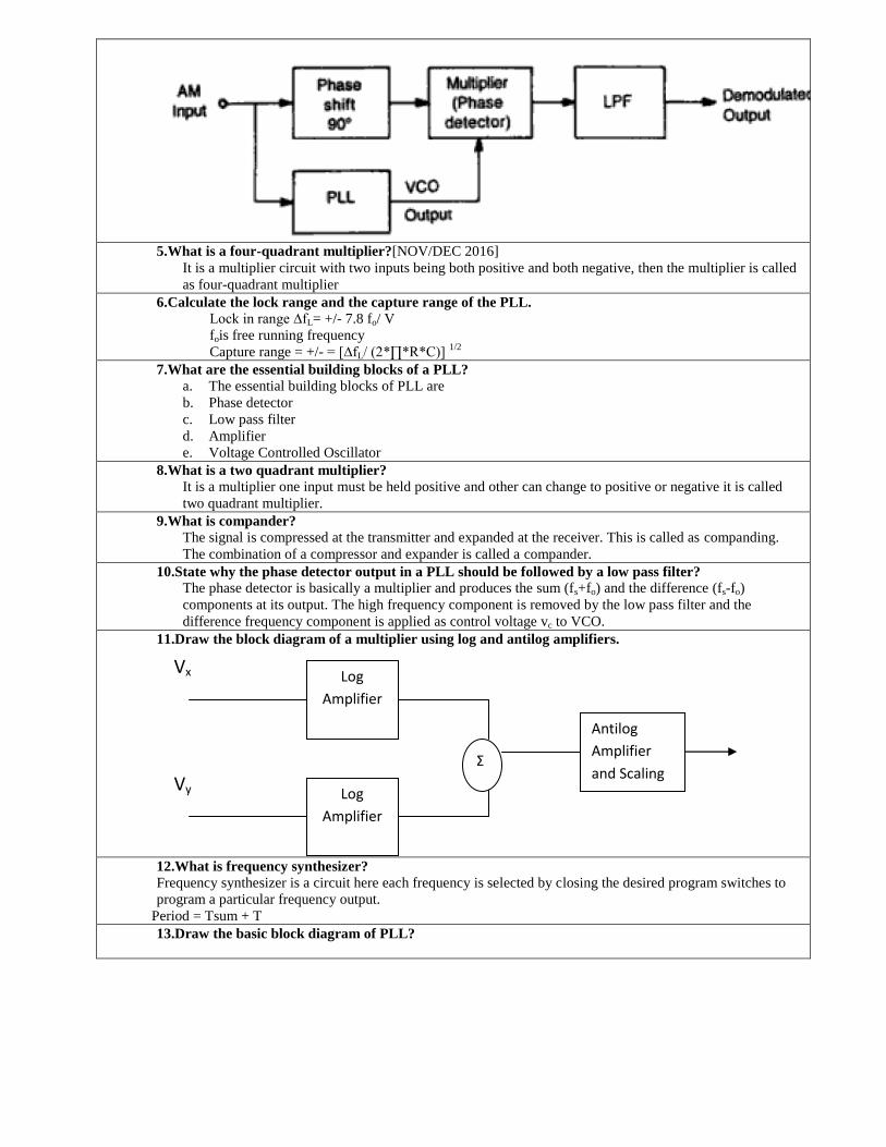
4.Draw the block diagram of PLL for AM detection? [APRIL/MAY 16]
5.What is a four-quadrant multiplier?[NOV/DEC 2016]
It is a multiplier circuit with two inputs being both positive and both negative, then the multiplier is called
as four-quadrant multiplier
6.Calculate the lock range and the capture range of the PLL.
Lock in range ∆fL= +/- 7.8 fo/ V
fois free running frequency
Capture range = +/- = [∆fL/ (2*∏*R*C)] 1/2
7.What are the essential building blocks of a PLL?
a. The essential building blocks of PLL are
b. Phase detector
c. Low pass filter
d. Amplifier
e. Voltage Controlled Oscillator
8.What is a two quadrant multiplier?
It is a multiplier one input must be held positive and other can change to positive or negative it is called
two quadrant multiplier.
9.What is compander?
The signal is compressed at the transmitter and expanded at the receiver. This is called as companding.
The combination of a compressor and expander is called a compander.
10.State why the phase detector output in a PLL should be followed by a low pass filter?
The phase detector is basically a multiplier and produces the sum (fs+fo) and the difference (fs-fo)
components at its output. The high frequency component is removed by the low pass filter and the
difference frequency component is applied as control voltage vc to VCO.
11.Draw the block diagram of a multiplier using log and antilog amplifiers.
12.What is frequency synthesizer?
Frequency synthesizer is a circuit here each frequency is selected by closing the desired program switches to
program a particular frequency output.
Period = Tsum + T
13.Draw the basic block diagram of PLL?
Log
Amplifier
Log
Amplifier
Σ
Antilog
Amplifier
and Scaling
Vx
Vy
14.What is amplitude modulation?
It is the process of amplitude of carrier wave varies in accordance with the instantaneous value of the
amplitude of message signal.
15.Define voltage to frequency conversion factor kv?
It is given as
Kv = ∆fo / ∆vc
Here Kv is the modulation voltage required to produce the frequency shift ∆fofor a VCO.
16.Give two application of PLL?
i. Frequency multiplication and division
ii. Frequency translation.
iii. AM detection.
iv. FM demodulation
17.What is a voltage-controlled oscillator?
A voltage controlled oscillator is an oscillator circuit in which the frequency of oscillation can be
controlled by an externally applied voltage. It provides the linear relationship between the applied voltage
and the oscillation frequency.
VCO is a free running multivibrator and operates at a set of frequency fo called free running frequency.
This frequency is determined by an external timing capacitor and an external resistor. It can also be shifted
to either side by applying a dc control voltage Vc to an appropriate terminal of the IC.The frequency
deviation is directly proportional to the dc control voltage and hence it is called a “Voltage Controlled
Oscillator”.
18.When an amplifier is also called an error amplifier?
An amplifier also called an error amplifier in control theory, which accepts the signal Xdand yields the
output signal X0=a.Xd, where a is the forward gain of the amplifier is called the open-loop gain of the
circuit.
19.What are the merits of companding?
The compression process reduces the dynamic range of the signal before it is
transmitted.
Companding preserves the signal to noise ratio of the original signal and avoids non linear distortion
of the signal when the input amplitude is large.
It also reduces buzz, bias and low level audio tones caused by mild interference.
20.List the applications of OTA:
OTA can be used in
programmable gain voltage amplifier
sample and hold circuits
voltage controlled state variable filter
current controlled relaxation oscillator
21.Mention some areas where PLL is widely used.
Radar synchronization
Satellite communication systems
Air borne navigational systems
FM communication systems
22.Define lock-in range of a PLL.
The range of frequencies over which the PLL can maintain lock with the incoming signal is called the lock-in
range or tracking range. It is expressed as a percentage of the VCO free running frequency
23.Define free running mode.
In a PLL if the error control voltage is zero then the PLL is said to be operated in free running mode and
its output frequency is called its center frequency f0.
24.What are the advantages of variable transconductance technique?
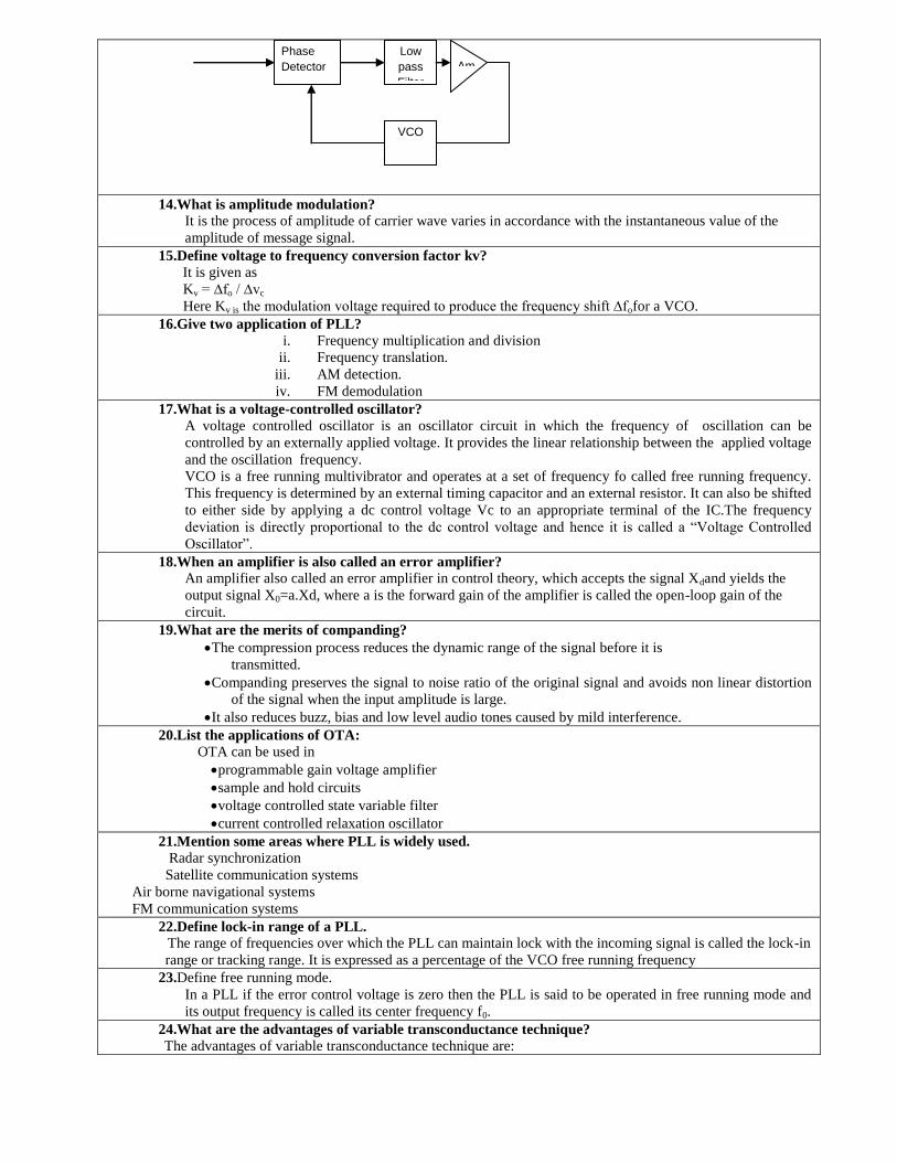
The advantages of variable transconductance technique are:
Phase
Detector
Low
pass
Filter
VCO
Am
p
1)Simple to integrate into monolithic chip
2)Provides very good accuracy.
3)Very cheap hence economical.
4)Provides four quadrant operations.
5)It provides high speed of operation which is 2 to 3 times more than the logarithmic method.
6)Reduced error at least by 10 times.
25.With reference to a VCO, define voltage to frequency conversion factor Kv.
Voltage to frequency conversion factor Kv is defind as Kv=Δfo/ Δvc
Here Δvc is the modulation voltage required to produce the frequency shift of Δfo for a VCO
26.Draw the relation between the capture ranges and lock range in a PLL.
27.Mention two applications of analog multiplier
Variable-gain amplifier
Ring modulator
Product detector
Frequency mixer
28.VCO is called as V-F converter why?
A voltage-controlled oscillator or VCO is an electronic oscillator whose oscillation frequency is controlled
by a voltage input ie the change in input voltage results in change in output frequency hence it is called as
V-F converter
29.Define FSK
Frequency shift keying is a digital modulation technique in which the frequency of carrier signal is varied
in accordance with the amplitude of digital modulating signal
30. What is the need for frequency synthesizer
A frequency synthesizer is an electronic system for generating any of a range of frequencies from a single
fixed time base or oscillator. They are found in many modern devices, including radio receivers, mobile
telephones, radiotelephones, walkie-talkies, CB radios, satellite receivers, GPS systems, etc
PART-B&C
1.With neat diagram explain the design of (i) Frequency Synthesizer (ii) Frequency Division circuit
using PLL IC 565[April/May 2017]
[Ref .Roy Choudhry, ShailB.Jain, “Linear Integrated Circuits (Fourth Edition)”, Page 342]
2.i) Discuss the principle of operation of NE 565 PLL circuit [Nov/Dec 2016]
[Ref .Roy Choudhry, ShailB.Jain, “Linear Integrated Circuits (Fourth Edition)”, Page 337]
ii)How can PLL be modeled as a frequency multiplier?[Nov/Dec 2016]
[Ref .Roy Choudhry, ShailB.Jain, “Linear Integrated Circuits (Fourth Edition)”, Page 342
3.Explain the Application of PLL as AM detection,FM detection and FSK demodulation [April/May 16]
[Ref .Roy Choudhry, Shail B.Jain, “Linear Integrated Circuits (Second Edition)”, Page 375]
4.Explain the basic blocks of PLL and determine expressions for lock in range and capture range
[April/May 15]
[Ref .Roy Choudhry, Shail B.Jain, “Linear Integrated Circuits (Second Edition)”, Page 353& 370]
5.i) With neat simplified internal diagram explain the working principle of Operational
Transconductance Amplifier(OTA)[April/May15]
[Ref .Roy Choudhry, Shail B.Jain, “Linear Integrated Circuits (Second Edition)”, Page 210]
ii) Explain the application of VCO for FM generation[April /May15
[Ref .Roy Choudhry, Shail B.Jain, “Linear Integrated Circuits (Second Edition)”, Page 225]
6.With suitable block diagram explain the operation of 566 voltage controlled oscillator. Also derive an
expression for the frequency of the output waveform generated[Nov/Dec 10]
[Ref .Roy Choudhry, Shail B.Jain, “Linear Integrated Circuits (Second Edition)”, Page 363]
7.Explain the working principle of four quadrant variable form transconductance multiplier [May/June
2016]
[Ref .Roy Choudhry, Shail B.Jain, “Linear Integrated Circuits (Second Edition)”, Page 210]
8.Draw the analog multiplier IC and explain its features and Explain the application of analog
multiplier IC[April/May 2015]
[Ref .Roy Choudhry, Shail B.Jain, “Linear Integrated Circuits (Second Edition)”, Page 183]
9.i)Explain Analog Multiplier using Emitter Coupled Transistor Pair
[Ref .Roy Choudhry, Shail B.Jain, “Linear Integrated Circuits (Second Edition)”, Page 183]
ii)Explain Gilbert Multiplier cell in detail
[Ref .Roy Choudhry, Shail B.Jain, “Linear Integrated Circuits (Second Edition)”, Page 183]
UNIT IV-ANALOG TO DIGITAL AND DIGITAL TO ANALOG CONVERTERS Analog and Digital Data Conversions, D/A converter – specifications - weighted resistor type, R-2R Ladder type,
Voltage Mode and Current-Mode R-2R Ladder types - switches for D/A converters, high speed sample-and-hold
circuits, A/D Converters – specifications - Flash type - Successive Approximation type - Single Slope type – Dual
Slope type - A/D Converter using Voltage-to-Time Conversion - Over-sampling A/D Converters. PART-B&C
1.How is the classification of A/D converters carried out based on their operational features? [Nov/Dec
2017]
A/D converter are classified into two groups according to their conversion
i)Direct type ADC
ii)Integrating type ADC
Direct Type ADC
(i)Flash Type converter
(ii)Counter type converter
(iii)Tracking or servo converter
(iv)Successive approximation type converter
Integrating type ADC
(i)Charge balancing ADC
(ii)Dual slope ADC
2.Find the number of resistors required for an 8 bit weighted resistor D/A converter. Consider the
smallest resistance is R and obtain those resistance values.[Nov/Dec 2017]
The No of Resistors required =8
The resistance values are 21R,2
2R,2
3R,2
4R,2
5R,2
6R,2
7R,2
8R
3.Why are Scottky diodes used in sample and hold circuits?[April/May 2017]
Schottky diodes can be used in diode-bridge based sample and hold circuits. When compared to
regular p-n junction based diode bridges, Schottky diodes can offer advantages. A forward-biased Schottky
diode does not have any minority carrier charge storage. This allows them to switch more quickly than regular
diodes, resulting in lower transition time from the sample to the hold step. The absence of minority carrier
charge storage also results in a lower hold step or sampling error, resulting in a more accurate sample at the
output
4.What are the advantages of inverted R-2R (current type) ladder D/A converter over R-2R (voltage
type) D/A converter?[Nov/Dec 2016]
In R-2R ladder type DAC current flowing in the resistors changes as the input data changes. More
power dissipation causes heating which in turn creates non-linearity in DAC.This problem can be avoided in
inverted R-2R ladder type as the current divides equally at each node.
5.What is the need for electronic switches in D/A converter?[Nov/Dec 2016]
The Switches which connects the digital binary input to the nodes of a D/A converter is an electronic
switch
6.A 12 bit D/A converter has a resolution of 20mv/LSB.Find the full scale output voltage.[May/June
2016]
Re2 1
oFS
n
Vsolution
Where, VoFS is the full scale output voltage
n is the number of bits
Re *(2 1)n
oFSV solution
3 1220*10 *(2 1)oFSV
81.9oFSV V
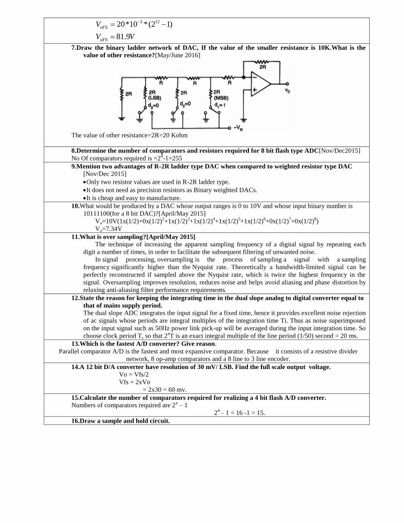
7.Draw the binary ladder network of DAC, If the value of the smaller resistance is 10K.What is the
value of other resistance?[May/June 2016]
The value of other resistance=2R=20 Kohm
8.Determine the number of comparators and resistors required for 8 bit flash type ADC[Nov/Dec2015]
No Of comparators required is =28-1=255
9.Mention two advantages of R-2R ladder type DAC when compared to weighted resistor type DAC
[Nov/Dec 2015]
Only two resistor values are used in R-2R ladder type.
It does not need as precision resistors as Binary weighted DACs.
It is cheap and easy to manufacture.
10.What would be produced by a DAC whose output ranges is 0 to 10V and whose input binary number is
10111100(for a 8 bit DAC)?[April/May 2015]
Vo=10V(1x(1/2)+0x(1/2)2+1x(1/2)
3+1x(1/2)
4+1x(1/2)
5+1x(1/2)
6+0x(1/2)
7+0x(1/2)
8)
Vo=7.34V
11.What is over sampling? [April/May 2015]
The technique of increasing the apparent sampling frequency of a digital signal by repeating each
digit a number of times, in order to facilitate the subsequent filtering of unwanted noise.
In signal processing, oversampling is the process of sampling a signal with a sampling
frequency significantly higher than the Nyquist rate. Theoretically a bandwidth-limited signal can be
perfectly reconstructed if sampled above the Nyquist rate, which is twice the highest frequency in the
signal. Oversampling improves resolution, reduces noise and helps avoid aliasing and phase distortion by
relaxing anti-aliasing filter performance requirements.
12.State the reason for keeping the integrating time in the dual slope analog to digital converter equal to
that of mains supply period.
The dual slope ADC integrates the input signal for a fixed time, hence it provides excellent noise rejection
of ac signals whose periods are integral multiples of the integration time Ti. Thus as noise superimposed
on the input signal such as 50Hz power link pick-up will be averaged during the input integration time. So
choose clock period T, so that 2nT is an exact integral multiple of the line period (1/50) second = 20 ms.
13.Which is the fastest A/D converter? Give reason.
Parallel comparator A/D is the fastest and most expansive comparator. Because it consists of a resistive divider
network, 8 op-amp comparators and a 8 line to 3 line encoder.
14.A 12 bit D/A converter have resolution of 30 mV/ LSB. Find the full scale output voltage.
Vo = Vfs/2
Vfs = 2xVo
= 2x30 = 60 mv.
15.Calculate the number of comparators required for realizing a 4 bit flash A/D converter.
Numbers of comparators required are 2n – 1
24 – 1 = 16 -1 = 15.
16.Draw a sample and hold circuit.
D
+
-
3
26
74
+
-
3
26
74
G
VC
VO
2
1 3
C
S
V1
17.Define resolution of a D/A converter?
The resolution of a DAC is defined as the smallest change in voltage, which may be produced at the
output or input of the converter.
18.How many comparators are required to build n –bit flash type A/D converter?
Comparator required to build n –bit flash type A/D converter is 2n – 1
Where n is the desired number of bits.
19.Define monotonicity with respect to D/A converter?
A DAC is said to be monotonic if the analog output increases or remains the same as the digital input
increases. This results in the output always being single – valued.
20.Why is R-2R ladder network DAC better than weighted resistor DAC?
Wide ranges of resistors are required in binary weighted resistor type DAC.
This can be avoided by using R-2R ladder type DAC.
i. Easier to build accurately as only two precision metal film resistors are required.
ii. Number of bits can be expanded by adding more sections of same R-2R values.
iii. In inverted R-2R ladder DAC, node voltages remain constant with changing input
binary words. This avoids any slowdown effects by stray capacitances.
21.Which type of ADC is used in all digital voltmeter?
Dual slope ADC converters are particularly suitable for accurate measurement of slowly varying signals,
such as digital panel meters and multimeters.
22.What do you mean by delta modulation?
Delta modulation is a method of information transmission with the help of pulses. It is one type of digital
modulation and it determines the increase or decrease of the signal sample with respect to previous
sample. And encodes this rise or fall of amplitude by 1 bit.
23.List the application of sample and Hold circuits?
i. It is used in ADC.
ii. It is used in digital interfacing
iii. It is used in pulse modulation system
iv.It is used in analog demultiplexer
24.Mention the types of DAC techniques?
ii. Weighted resistance
iii. Inverted R_2R ladder
iv.Multiplying.
25.Define the resolution of DAC?
Resolution of DAC is defined as the change in the output voltage corresponding to the change of one bit in
the digital input.
26.Explain in brief stability of a converter:
The performance of converter changes with temperature age & power supply variation . So all the relevant
parameters such as offset, gain, linearity error& monotonicity must be specified over the full temperature
& power supply ranges to have better stability performances.
27.What is meant by linearity?
The linearity of an ADC/DAC is an important measure of its accuracy & tells us how close the converter
output is to its ideal transfer characteristics. The linearity error is usually expressed as a fraction of LSB
increment or percentage of full-scale voltage. A good converter exhibits a linearity error of less than
±½LSB.
28.What is monotonic DAC?
A monotonic DAC is one whose analog output increases for an increase in digital input.
29.What is multiplying DAC?
A digital to analog converter which uses a varying reference voltage VR is called a multiplying DAC
(MDAC). If the reference voltage of a DAC, VR is a sine wave given by:
V(t) = Vin Cos 2πft;
Then, Vo(t) = Vom Cos (2πft + 180o)
30.What is a sample and hold circuit? Where it is used?
A sample and hold circuit is one which samples an input signal and holds on to its last sampled value until
the input is sampled again. This circuit is mainly used in digital interfacing, analog to digital systems, and
pulse code modulation systems.
31.Define sample period and hold period.
The time during which the voltage across the capacitor in sample and hold circuit is equal to the input
voltage is called sample period. The time period during which the voltage across the capacitor is held
constant is called hold period.
32.Define accuracy of converter.
Absolute accuracy:
It is the maximum deviation between the actual converter output & the ideal converter output.
Relative accuracy:
It is the maximum deviation after gain & offset errors have been removed. The accuracy of a converter
is also specified in form of LSB increments or % of full scale voltage.
33.What output voltage would be produced by a D/A converter whose output range is 0 to 10 V and
whose input binary number is 0110 for a 4 bit DAC.
Given
The output voltage at 0110=0.6667*6=4V
34.What is the main drawback of dual slope ADC?
The conversion time of dual slope ADC is high .This is the main drawback of dual slope ADC.
35.Define settling time
It is the time the converter takes for the output to settle within a specified band +/-(1/2)LSB
36.A 12 bit D/A converter has resolution of 20mV/LSB.Find the full scale output voltage[APRIL/MAY
16]
Given resolution = 20mV/LSB
Full scale output voltage =Resolution(1012
-1)=20*10-3
(1012
-1)
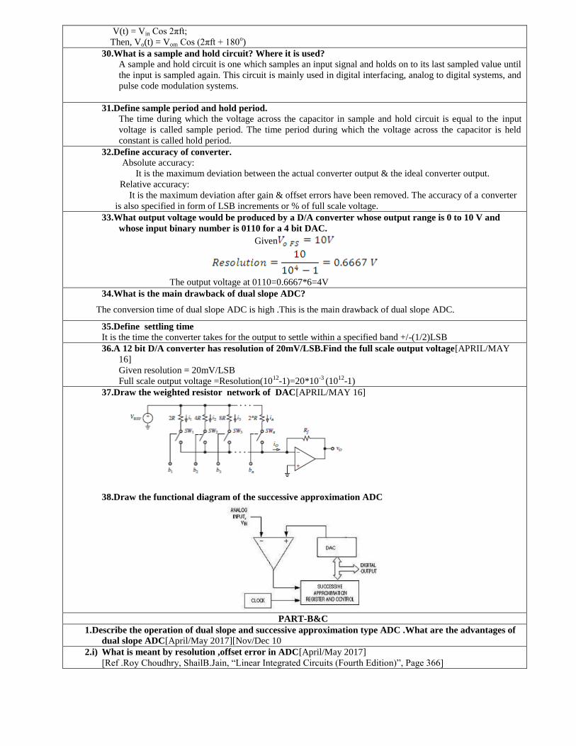
37.Draw the weighted resistor network of DAC[APRIL/MAY 16]
38.Draw the functional diagram of the successive approximation ADC
PART-B&C
1.Describe the operation of dual slope and successive approximation type ADC .What are the advantages of
dual slope ADC[April/May 2017][Nov/Dec 10
2.i) What is meant by resolution ,offset error in ADC[April/May 2017]
[Ref .Roy Choudhry, ShailB.Jain, “Linear Integrated Circuits (Fourth Edition)”, Page 366]
ii)Discuss on the single slope type ADC
[Ref .Roy Choudhry, ShailB.Jain, “Linear Integrated Circuits (Fourth Edition)”, Page 363]
3.i) Explain the successive approximation type A/D converter[APRIL/MAY 16]
[Ref .Roy Choudhry, Shail B.Jain, “Linear Integrated Circuits (Second Edition)”, Page 396]
ii) Narrate the functions of Analog switches
[Ref .Roy Choudhry, Shail B.Jain, “Linear Integrated Circuits (Second Edition)”, Page 383]
4.i)How are A/D converters categorized? [April/May 2017]
[Ref .Roy Choudhry, Shail B.Jain, “Linear Integrated Circuits (Second Edition)”, Page 393]
ii)Write Short Note on high speed sample and hold circuits[April/May 15] [April/May 16] (6)
[Ref .Roy Choudhry, Shail B.Jain, “Linear Integrated Circuits (Second Edition)”, Page 176]
5.i) Explain voltage mode and current mode operations of R-2R ladder type DAC[Nov/Dec 10]
[Ref .Roy Choudhry, Shail B.Jain, “Linear Integrated Circuits (Second Edition)”, Page 386]
ii)Explain over sampling type analog to digital converters
[Ref .Roy Choudhry, Shail B.Jain, “Linear Integrated Circuits (Second Edition)”, Page 176]
6.Draw the block diagram and explain the working of
i)Charge Balancing VFCS(8)
[Ref .Roy Choudhry, Shail B.Jain, “Linear Integrated Circuits (Second Edition)”, Page 225]
ii)Voltage to Time converter(8)[May/June 13]
[Ref .Roy Choudhry, Shail B.Jain, “Linear Integrated Circuits (Second Edition)”, Page 225]
7.Explain the following type DAC with suitable diagrams
i)Binary weighted resistor DAC(6)
[Ref .Roy Choudhry, Shail B.Jain, “Linear Integrated Circuits (Second Edition)”, Page 382]
ii)R-2R Ladder DAC(5)
[Ref .Roy Choudhry, Shail B.Jain, “Linear Integrated Circuits (Second Edition)”, Page 385]
iii)Inverted R-2R ladder DAC(5)[Nov/Dec 11]
[Ref .Roy Choudhry, Shail B.Jain, “Linear Integrated Circuits (Second Edition)”, Page 386]
8.i) Explain the following type of electronic switches used in D/A converter with suitable
diagrams
1.Totem pole MOSFET switch(4)
2.CMOS inverter as a switch(4)[May/June 12]
[Ref .Roy Choudhry, Shail B.Jain, “Linear Integrated Circuits (Second Edition)”, Page 384]
ii) Compare Flash type ,Dual slope and successive approximation ADC in terms of parameters like
speed ,accuracy, resolution ,input hold time(8)[May/June 12]
[Ref .Roy Choudhry, Shail B.Jain, “Linear Integrated Circuits (Second Edition)”, Page 393]
9.With a neat block diagram explain the working of three bit flash type analog to digital converter
[Ref .Roy Choudhry, Shail B.Jain, “Linear Integrated Circuits (Second Edition)”, Page 393]
UNIT V-WAVEFORM GENERATORS AND SPECIAL FUNCTION ICS
Sine-wave generators, Multivibrators and Triangular wave generator, Saw-tooth wave generator, ICL8038 function
generator, Timer IC 555, IC Voltage regulators – Three terminal fixed and adjustable voltage regulators - IC 723
general purpose regulator - Monolithic switching regulator, Switched capacitor filter IC MF10, Frequency to Voltage
and Voltage to Frequency converters, Audio Power amplifier, Video Amplifier, Isolation Amplifier, Opto-couplers
and fibre optic IC
PART-A
1.Define current transfer ratio of an opto coupler[Nov/Dec 2017]
The current transfer ratio (CTR) is a parameter similar to the DC current amplification ratio of a transistor
(hFE) and is expressed as a percentage indicating the ratio of the output current (IC) to the input current (IF).
CTR(%)=(IC/IF) x 100
2.Draw a fixed voltage regulator circuit and state its operation[Nov/Dec 2017]
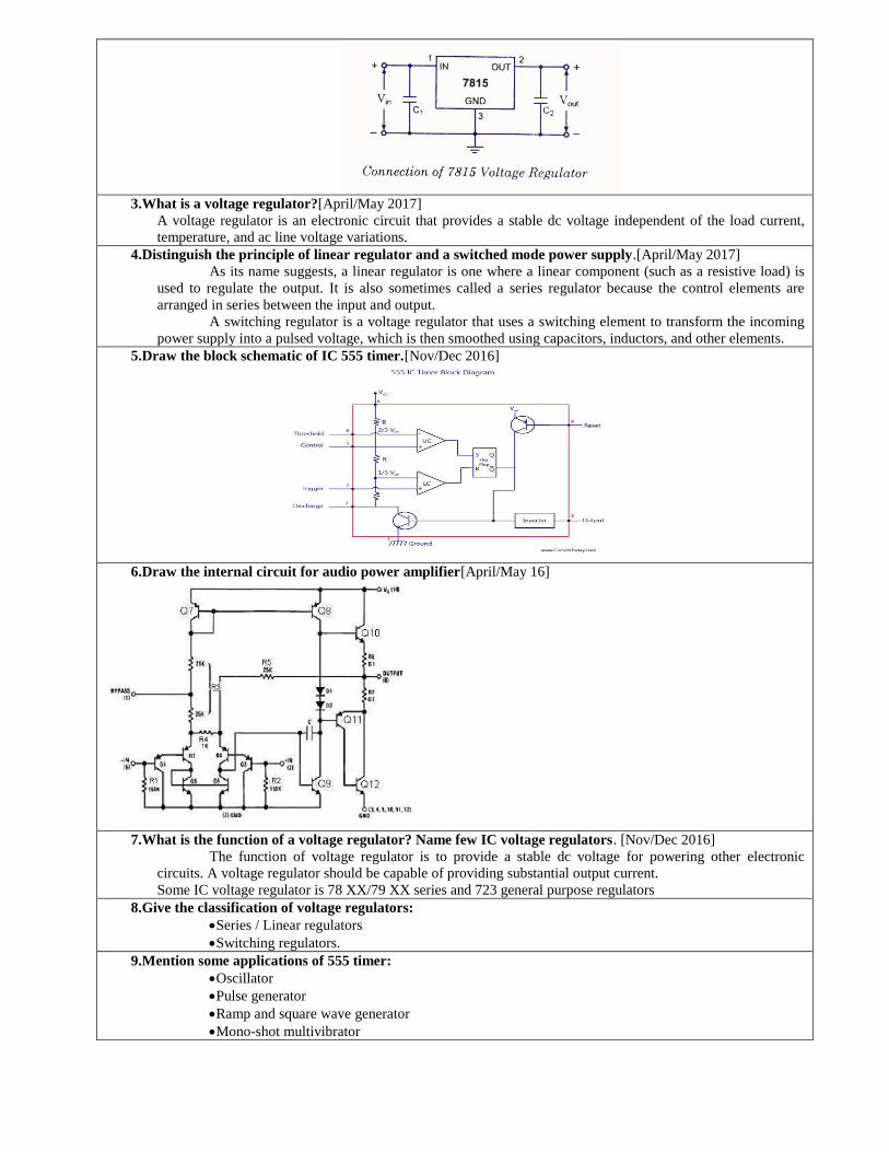
3.What is a voltage regulator?[April/May 2017]
A voltage regulator is an electronic circuit that provides a stable dc voltage independent of the load current,
temperature, and ac line voltage variations.
4.Distinguish the principle of linear regulator and a switched mode power supply.[April/May 2017]
As its name suggests, a linear regulator is one where a linear component (such as a resistive load) is
used to regulate the output. It is also sometimes called a series regulator because the control elements are
arranged in series between the input and output.
A switching regulator is a voltage regulator that uses a switching element to transform the incoming
power supply into a pulsed voltage, which is then smoothed using capacitors, inductors, and other elements.
5.Draw the block schematic of IC 555 timer.[Nov/Dec 2016]
6.Draw the internal circuit for audio power amplifier[April/May 16]
7.What is the function of a voltage regulator? Name few IC voltage regulators. [Nov/Dec 2016]
The function of voltage regulator is to provide a stable dc voltage for powering other electronic
circuits. A voltage regulator should be capable of providing substantial output current.
Some IC voltage regulator is 78 XX/79 XX series and 723 general purpose regulators
8.Give the classification of voltage regulators:
Series / Linear regulators
Switching regulators.
9.Mention some applications of 555 timer:
Oscillator
Pulse generator
Ramp and square wave generator
Mono-shot multivibrator
Burglar alarm
Traffic light control.
10.List the applications of 555 timer in monostable mode of operation:
Missing pulse detector
Linear ramp generator
Frequency divider
Pulse width modulation.
11.List the applications of 555 timer in Astable mode of operation:
FSK generator
Pulse-position modulator
12.What is a linear voltage regulator?
Series or linear regulator uses a power transistor connected in series between the unregulated dc input and the
load and it conducts in the linear region. The output voltage is controlled by the continuous voltage drop
taking place across the series pass transistor.
13.What is a switching regulator?
Switching regulators are those which operate the power transistor as a high frequency on/off switch, so
that the power transistor does not conduct current continuously. This gives improved efficiency over series
regulators.
14.What is the purpose of having input and output capacitors in three terminal IC regulators?
A capacitor connected between the input terminal and ground cancels the inductive effects due to long distribution
leads. The output capacitor improves the transient response.
15.Define line regulation.
Line regulation is defined as the percentage change in the output voltage for a change in the input voltage. It is
expressed in millivolts or as a percentage of the output voltage.
16.Define load regulation.
Load regulation is defined as the change in output voltage for a change in load current. It is expressed in
millivolts or as a percentage of the output voltage.
17.What is meant by current limiting?
Current limiting refers to the ability of a regulator to prevent the load current from increasing above a preset
value.
18.Give the drawbacks of linear regulators:
The input step down transformer is bulky and expensive because of low line frequency.
Because of low line frequency, large values of filter capacitors are required to decrease the ripple.
Efficiency is reduced due to the continuous power dissipation by the transistor as it operates in the
linear region.
19.What is the advantage of switching regulators?
Greater efficiency is achieved as the power transistor is made to operate as low impedance switch.
Power transmitted across the transistor is in discrete pulses rather than as a steady current flow.
By using suitable switching loss reduction technique, the switching frequency can be increased so as to
reduce the size and weight of the inductors and capacitors.
20.What is an opto-coupler IC? Give examples.
Opto-coupler IC is a combined package of a photo-emitting device and a photo sensing device.
Examples for opto-coupler circuit :LED and a photo diode,
LED and photo transistor,
LED and Darlington.
Examples for opto-coupler IC : MCT 2F , MCT 2E
21.Mention the advantages of opto-couplers:
Better isolation between the two stages.
Impedance problem between the stages is eliminated.
Wide frequency response.
Easily interfaced with digital circuit.
Compact and light weight.
Problems such as noise, transients, contact bounce are eliminated.
22.What is an isolation amplifier?
An isolation amplifier is an amplifier that offers electrical isolation between its input and output terminals.
23.What is the need for a tuned amplifier?
In radio or TV receivers, it is necessary to select a particular channel among all other available channels.
Hence some sort of frequency selective circuit is needed thatwill allow us to amplify the frequency band

required and reject all the other unwanted signals and this function is provided by a tuned amplifier.
24.Give the classification of tuned amplifier:
(i) Small signal tuned amplifier
Single tuned
Double tuned
Stagger tuned
(ii) Large signal tuned amplifier.
25.Draw the functional block diagram of 723 regulator.
26.Why is the monostable multivibrator circuit called time delay circuit and gating circuit?
Monostable multivibrator circuit called time delay circuit because it generates a fast transition at a
predetermined time T after the application of input trigger. It is called as a gating circuit because it generates
rectangular waveform at a definite time and could be used as gate parts of a system.
27.Why there is no phase shift provided in the feedback network in Wein-Bridge oscillator?
In Wein-bridge oscillator, the feedback signal is connected to the (+) input terminal so that, the op-amp is
working as a non-inverting amplifier, which produces 0 degree or 360 degree phase shift.. Therefore the
feedback network need not provide any phase shift.
28.Give the formula for period of oscillations in an op-amp astable circuit.
The formula for period of oscillations in an op-amp astable circuit is
29.Define duty cycle for a periodic pulse waveform.
The duty cycle of the output pulse waveform is given by
30.What is meant by thermal shutdown applied to voltage regulators?
Due to overheating , the series pass element of regulator may get damaged. To avoid this, thermal shutdown is
provided. In this protection scheme, the junction temperature of the series pass element is sensed. By sensing
this, its power dissipation is reduced by using certain circuit till its temperature drops to a lower safe value.
31.What are the three waveforms generated by ICL8038?
Sine wave
Square wave
triangular Wave
32.List the characteristics of optocoupler
(i) Current Transfer Ratio:
(ii) Isolation voltage between input & output:
(iii) Response Time:
(iv) Common mode Rejection:
33. Mention two applications of frequency to voltage converter
Frequency to voltage converter in tachometers.
Frequency difference measurement.
34. What is the advantage of switching regulators?
Switching regulators are highly efficient and able to step up (boost), step down (buck), and invert voltages
with ease
Switching regulators are efficient because the series element is either fully conducting or switched off because
it dissipates almost no power. Switching regulators are able to generate output voltages that are higher than the
input voltage or of opposite polarity, unlike linear regulators.
PART-B&C
1.i) With neat diagram explain the operation of an astable and monostable multivibrators[Nov/Dec 2017]
[Ref .Roy Choudhry, ShailB.Jain, “Linear Integrated Circuits (Fourth Edition)”, Page 216 &318]
ii)Draw the functional diagram and connection diagram of a low voltage regulator and explain[Nov/Dec
2017]
[Ref .Roy Choudhry, ShailB.Jain, “Linear Integrated Circuits (Fourth Edition)”, Page 241]
2.Answer any two of the following[April/May 2017]
i)Switched capacitor filters
[Ref .Roy Choudhry, ShailB.Jain, “Linear Integrated Circuits (Fourth Edition)”, Page 288]
ii)Audio power amplifier
[Ref .Roy Choudhry, ShailB.Jain, “Linear Integrated Circuits (Fourth Edition)”, Page 322]
iii)Opto coupler
[Ref .Roy Choudhry, ShailB.Jain, “Linear Integrated Circuits (Fourth Edition)”, Page 322]
2.With neat diagram explain IC723 general purpose voltage regulator[May/June 14] [April/May 16]
[Ref .Roy Choudhry, Shail B.Jain, “Linear Integrated Circuits (Second Edition)”, Page 272]
3.Explain Sawtooth waveform generator and LM 380Audio amplifier in detail [April/May 16]
[Ref .Roy Choudhry, Shail B.Jain, “Linear Integrated Circuits (Second Edition)”, Page 247]
4.Describe the working of a astable multivibrator using 555 timer[Nov/Dec 11] [April/May 16]
[Ref .Roy Choudhry, Shail B.Jain, “Linear Integrated Circuits (Second Edition)”, Page 345]
5.Explain in detail Voltage to frequency and frequency to voltage converter[May/June 14]
[Ref. Sergio Franco, “Design with Operational Amplifiers and Analog Integrated Circuits”, 3rd Edition page
520
6.i)Design a phase shift oscillate at 100Hz (May/June 15)
[Ref .Roy Choudhry, Shail B.Jain, “Linear Integrated Circuits (Second Edition)”, Page 250]
ii) Describe monostable multivibrator with necessary diagrams and derive for ON time and recovery
time[May/June 15]
[Ref .Roy Choudhry, Shail B.Jain, “Linear Integrated Circuits (Second Edition)”, Page 337]
7.i)Briefly describe about monolithic switching regulators[April/May 15]
[Ref .Roy Choudhry, Shail B.Jain, “Linear Integrated Circuits (Second Edition)”, Page 280]
ii)Draw the schematic of ICL 8038 function generator and discuss its features (8) [April/May 15]
[Ref .Roy Choudhry, Shail B.Jain, “Linear Integrated Circuits (Second Edition)”, Page 225]
8.Describe the working of a Astable multivibrator using op-amp [Nov/Dec 14]
[Ref .Roy Choudhry, Shail B.Jain, “Linear Integrated Circuits (Second Edition)”, Page 241]
9.Describe the working of a monostable multivibrator using 555 timer[Nov/Dec 13]
[Ref .Roy Choudhry, Shail B.Jain, “Linear Integrated Circuits (Second Edition)”, Page 337]
10.Explain Video amplifier and opto-couplers
[Ref .Roy Choudhry, Shail B.Jain, “Linear Integrated Circuits (Second Edition)”, Page 380]
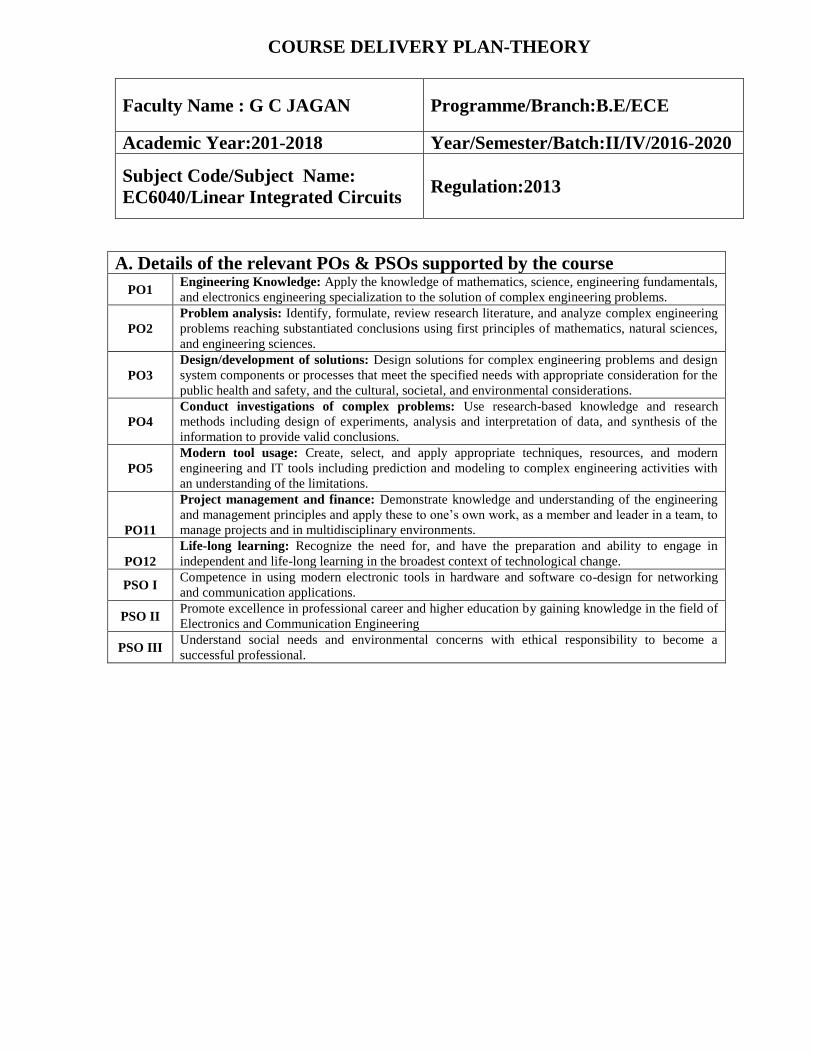
COURSE DELIVERY PLAN-THEORY
Faculty Name : G C JAGAN
Programme/Branch:B.E/ECE
Academic Year:201-2018 Year/Semester/Batch:II/IV/2016-2020
Subject Code/Subject Name:
EC6040/Linear Integrated Circuits
Regulation:2013
A. Details of the relevant POs & PSOs supported by the course
PO1 Engineering Knowledge: Apply the knowledge of mathematics, science, engineering fundamentals,
and electronics engineering specialization to the solution of complex engineering problems.
PO2
Problem analysis: Identify, formulate, review research literature, and analyze complex engineering
problems reaching substantiated conclusions using first principles of mathematics, natural sciences,
and engineering sciences.
PO3
Design/development of solutions: Design solutions for complex engineering problems and design
system components or processes that meet the specified needs with appropriate consideration for the
public health and safety, and the cultural, societal, and environmental considerations.
PO4
Conduct investigations of complex problems: Use research-based knowledge and research
methods including design of experiments, analysis and interpretation of data, and synthesis of the
information to provide valid conclusions.
PO5
Modern tool usage: Create, select, and apply appropriate techniques, resources, and modern
engineering and IT tools including prediction and modeling to complex engineering activities with
an understanding of the limitations.
PO11
Project management and finance: Demonstrate knowledge and understanding of the engineering
and management principles and apply these to one’s own work, as a member and leader in a team, to
manage projects and in multidisciplinary environments.
PO12
Life-long learning: Recognize the need for, and have the preparation and ability to engage in
independent and life-long learning in the broadest context of technological change.
PSO I Competence in using modern electronic tools in hardware and software co-design for networking
and communication applications.
PSO II Promote excellence in professional career and higher education by gaining knowledge in the field of
Electronics and Communication Engineering
PSO III Understand social needs and environmental concerns with ethical responsibility to become a
successful professional.
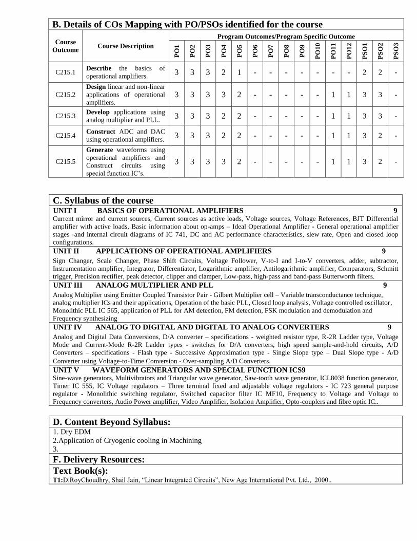
B. Details of COs Mapping with PO/PSOs identified for the course
Course
Outcome Course Description
Program Outcomes/Program Specific Outcome
PO
1
PO
2
PO
3
PO
4
PO
5
PO
6
PO
7
PO
8
PO
9
PO
10
PO
11
PO
12
PS
O1
PS
O2
PS
O3
C215.1 Describe the basics of
operational amplifiers. 3 3 3 2 1 - - - - - - - 2 2 -
C215.2
Design linear and non-linear
applications of operational
amplifiers. 3 3 3 3 2 - - - - - 1 1 3 3 -
C215.3 Develop applications using
analog multiplier and PLL. 3 3 3 2 2 - - - - - 1 1 3 3 -
C215.4 Construct ADC and DAC
using operational amplifiers. 3 3 3 2 2 - - - - - 1 1 3 2 -
C215.5
Generate waveforms using
operational amplifiers and
Construct circuits using
special function IC’s.
3 3 3 3 2 - - - - - 1 1 3 2 -
C. Syllabus of the course
UNIT I BASICS OF OPERATIONAL AMPLIFIERS 9 Current mirror and current sources, Current sources as active loads, Voltage sources, Voltage References, BJT Differential
amplifier with active loads, Basic information about op-amps – Ideal Operational Amplifier - General operational amplifier
stages -and internal circuit diagrams of IC 741, DC and AC performance characteristics, slew rate, Open and closed loop
configurations.
UNIT II APPLICATIONS OF OPERATIONAL AMPLIFIERS 9 Sign Changer, Scale Changer, Phase Shift Circuits, Voltage Follower, V-to-I and I-to-V converters, adder, subtractor,
Instrumentation amplifier, Integrator, Differentiator, Logarithmic amplifier, Antilogarithmic amplifier, Comparators, Schmitt
trigger, Precision rectifier, peak detector, clipper and clamper, Low-pass, high-pass and band-pass Butterworth filters.
UNIT III ANALOG MULTIPLIER AND PLL 9 Analog Multiplier using Emitter Coupled Transistor Pair - Gilbert Multiplier cell – Variable transconductance technique,
analog multiplier ICs and their applications, Operation of the basic PLL, Closed loop analysis, Voltage controlled oscillator,
Monolithic PLL IC 565, application of PLL for AM detection, FM detection, FSK modulation and demodulation and
Frequency synthesizing
UNIT IV ANALOG TO DIGITAL AND DIGITAL TO ANALOG CONVERTERS 9 Analog and Digital Data Conversions, D/A converter – specifications - weighted resistor type, R-2R Ladder type, Voltage
Mode and Current-Mode R-2R Ladder types - switches for D/A converters, high speed sample-and-hold circuits, A/D
Converters – specifications - Flash type - Successive Approximation type - Single Slope type – Dual Slope type - A/D
Converter using Voltage-to-Time Conversion - Over-sampling A/D Converters.
UNIT V WAVEFORM GENERATORS AND SPECIAL FUNCTION ICS9 Sine-wave generators, Multivibrators and Triangular wave generator, Saw-tooth wave generator, ICL8038 function generator,
Timer IC 555, IC Voltage regulators – Three terminal fixed and adjustable voltage regulators - IC 723 general purpose
regulator - Monolithic switching regulator, Switched capacitor filter IC MF10, Frequency to Voltage and Voltage to
Frequency converters, Audio Power amplifier, Video Amplifier, Isolation Amplifier, Opto-couplers and fibre optic IC..
D. Content Beyond Syllabus:
1. Dry EDM
2.Application of Cryogenic cooling in Machining
3.
F. Delivery Resources:
Text Book(s): T1:D.RoyChoudhry, Shail Jain, “Linear Integrated Circuits”, New Age International Pvt. Ltd., 2000..
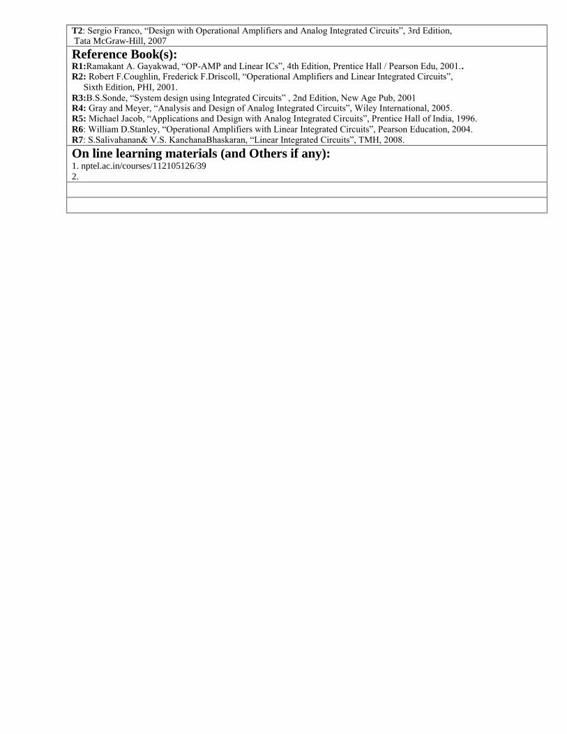
T2: Sergio Franco, “Design with Operational Amplifiers and Analog Integrated Circuits”, 3rd Edition, Tata McGraw-Hill, 2007
Reference Book(s): R1:Ramakant A. Gayakwad, “OP-AMP and Linear ICs”, 4th Edition, Prentice Hall / Pearson Edu, 2001.. R2: Robert F.Coughlin, Frederick F.Driscoll, “Operational Amplifiers and Linear Integrated Circuits”,
Sixth Edition, PHI, 2001.
R3:B.S.Sonde, “System design using Integrated Circuits” , 2nd Edition, New Age Pub, 2001 R4: Gray and Meyer, “Analysis and Design of Analog Integrated Circuits”, Wiley International, 2005. R5: Michael Jacob, “Applications and Design with Analog Integrated Circuits”, Prentice Hall of India, 1996.
R6: William D.Stanley, “Operational Amplifiers with Linear Integrated Circuits”, Pearson Education, 2004.
R7: S.Salivahanan& V.S. KanchanaBhaskaran, “Linear Integrated Circuits”, TMH, 2008.
On line learning materials (and Others if any): 1. nptel.ac.in/courses/112105126/39
2.
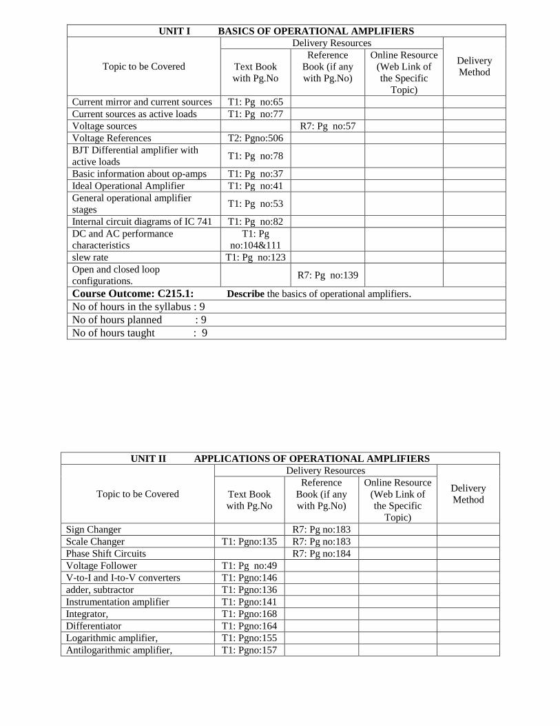
UNIT I BASICS OF OPERATIONAL AMPLIFIERS
Topic to be Covered
Delivery Resources
Delivery
Method Text Book
with Pg.No
Reference
Book (if any
with Pg.No)
Online Resource
(Web Link of
the Specific
Topic)
Current mirror and current sources T1: Pg no:65
Current sources as active loads T1: Pg no:77
Voltage sources R7: Pg no:57
Voltage References T2: Pgno:506
BJT Differential amplifier with
active loads T1: Pg no:78
Basic information about op-amps T1: Pg no:37
Ideal Operational Amplifier T1: Pg no:41
General operational amplifier
stages T1: Pg no:53
Internal circuit diagrams of IC 741 T1: Pg no:82
DC and AC performance
characteristics
T1: Pg
no:104&111
slew rate T1: Pg no:123
Open and closed loop
configurations. R7: Pg no:139
Course Outcome: C215.1: Describe the basics of operational amplifiers.
No of hours in the syllabus : 9
No of hours planned : 9
No of hours taught : 9
UNIT II APPLICATIONS OF OPERATIONAL AMPLIFIERS
Topic to be Covered
Delivery Resources
Delivery
Method Text Book
with Pg.No
Reference
Book (if any
with Pg.No)
Online Resource
(Web Link of
the Specific
Topic)
Sign Changer R7: Pg no:183
Scale Changer T1: Pgno:135 R7: Pg no:183
Phase Shift Circuits R7: Pg no:184
Voltage Follower T1: Pg no:49
V-to-I and I-to-V converters T1: Pgno:146
adder, subtractor T1: Pgno:136
Instrumentation amplifier T1: Pgno:141
Integrator, T1: Pgno:168
Differentiator T1: Pgno:164
Logarithmic amplifier, T1: Pgno:155
Antilogarithmic amplifier, T1: Pgno:157
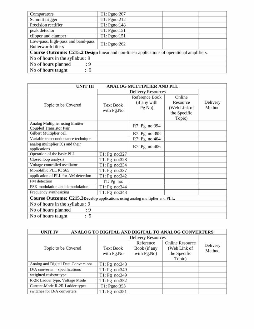
Comparators T1: Pgno:207
Schmitt trigger T1: Pgno:212
Precision rectifier T1: Pgno:148
peak detector T1: Pgno:151
clipper and clamper T1: Pgno:151
Low-pass, high-pass and band-pass
Butterworth filters T1: Pgno:262
Course Outcome: C215.2 Design linear and non-linear applications of operational amplifiers.
No of hours in the syllabus : 9
No of hours planned : 9
No of hours taught : 9
UNIT III ANALOG MULTIPLIER AND PLL
Topic to be Covered
Delivery Resources
Delivery
Method Text Book
with Pg.No
Reference Book
(if any with
Pg.No)
Online
Resource
(Web Link of
the Specific
Topic) Analog Multiplier using Emitter
Coupled Transistor Pair R7: Pg no:394
Gilbert Multiplier cell R7: Pg no:398 Variable transconductance technique R7: Pg no:404 analog multiplier ICs and their
applications R7: Pg no:406
Operation of the basic PLL T1: Pg no:327 Closed loop analysis T1: Pg no:328 Voltage controlled oscillator T1: Pg no:334 Monolithic PLL IC 565 T1: Pg no:337 application of PLL for AM detection T1: Pg no:342 FM detection T1: Pg no: FSK modulation and demodulation T1: Pg no:344 Frequency synthesizing T1: Pg no:343
Course Outcome: C215.3Develop applications using analog multiplier and PLL.
No of hours in the syllabus : 9
No of hours planned : 9
No of hours taught : 9
UNIT IV ANALOG TO DIGITAL AND DIGITAL TO ANALOG CONVERTERS
Topic to be Covered
Delivery Resources
Delivery
Method Text Book
with Pg.No
Reference
Book (if any
with Pg.No)
Online Resource
(Web Link of
the Specific
Topic) Analog and Digital Data Conversions T1: Pg no:348 D/A converter – specifications T1: Pg no:349 weighted resistor type T1: Pg no:349 R-2R Ladder type, Voltage Mode T1: Pg no:352 Current-Mode R-2R Ladder types T1: Pgno:353 switches for D/A converters T1: Pg no:351
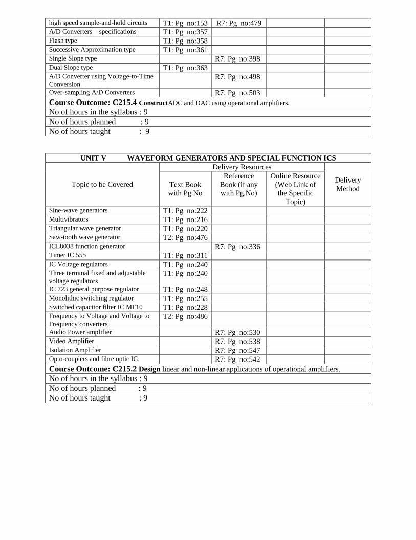
high speed sample-and-hold circuits T1: Pg no:153 R7: Pg no:479 A/D Converters – specifications T1: Pg no:357 Flash type T1: Pg no:358 Successive Approximation type T1: Pg no:361 Single Slope type R7: Pg no:398 Dual Slope type T1: Pg no:363 A/D Converter using Voltage-to-Time
Conversion
R7: Pg no:498
Over-sampling A/D Converters R7: Pg no:503
Course Outcome: C215.4 ConstructADC and DAC using operational amplifiers.
No of hours in the syllabus : 9
No of hours planned : 9
No of hours taught : 9
UNIT V WAVEFORM GENERATORS AND SPECIAL FUNCTION ICS
Topic to be Covered
Delivery Resources
Delivery
Method Text Book
with Pg.No
Reference
Book (if any
with Pg.No)
Online Resource
(Web Link of
the Specific
Topic) Sine-wave generators T1: Pg no:222 Multivibrators T1: Pg no:216 Triangular wave generator T1: Pg no:220 Saw-tooth wave generator T2: Pg no:476 ICL8038 function generator R7: Pg no:336 Timer IC 555 T1: Pg no:311 IC Voltage regulators T1: Pg no:240 Three terminal fixed and adjustable
voltage regulators T1: Pg no:240
IC 723 general purpose regulator T1: Pg no:248 Monolithic switching regulator T1: Pg no:255 Switched capacitor filter IC MF10 T1: Pg no:228 Frequency to Voltage and Voltage to
Frequency converters T2: Pg no:486
Audio Power amplifier R7: Pg no:530 Video Amplifier R7: Pg no:538 Isolation Amplifier R7: Pg no:547 Opto-couplers and fibre optic IC. R7: Pg no:542
Course Outcome: C215.2 Design linear and non-linear applications of operational amplifiers.
No of hours in the syllabus : 9
No of hours planned : 9
No of hours taught : 9