Embed Size (px)
Citation preview
-^V'5 Balanced Modulator-*VVirts.-page %;,.4f 1 27 0ct 75
'ARTS LIST * AP.-315 * BALANCED MODULATOR
NUMBER ■QUANTITYA 1 f
DESCRIPTION VALUE AND RATINGS
CI, 2 2 C a p a c i t o r , D i s c 0 . 1 m f d , 2 5 v0 3 1 i i ' i 3 3 p f0 4,5 n " 3 30 pf511, 16 , 17, 18
4 P o t e n t i o m e t e r , 1 / 4 " s h a f t 1 0 0 k l i n e a rR 2 , 3 , 4 , 5, 14 , 15f - ' / - f - ' j 6 R e s i s t o r , C a r b o n 10k 10%R 6 , 1 9 , 2 2 3 i i i i 3.3k 10%R9 1 i t i i 12k 10%' : 8 , 1 0 , 11 21
/ T r i m p o t 1 0 k l i n e a rR 1 2 , 1 3 n R e s i s t o r , C a r b o n 2.2k 10%A 7 1 i i i i 6.8k 10%':2 3 1 Re sis tor,C arbon 2 2k .10%R 2 4 , 2 5 0 i i n Ik 3 0%.
120 1 A t I t 15k 10%
Ul 1 I C M u l t i p l i e r MC1595 (Motoro la)U2 1
11412
66
O p e r a t i o n a l A m p l i fi e r
P r i n t e d C i r c u i t B o a r dF r o n t P a n e lK n o b s , 1 / 4 " S h a f tFrameB r a c k e t
Screw, 4 -40 x 3 /8NutS
LM301A
12 Jack, mini-phone
3 « . •■
( )
AR315 Balanced ModulatorASSEMBLYpaqo 1 of 4
A R I E S S y s t e m 5 0 0 M u s i c S y n t h e s i s e r 2 7 O c t 7 5Module AR 315
Balanced Modulator and Attenuators Assembly Instruction?
The previous pages were written as a general guide, to familiarize the■builder with the components. Here, now, are the specific assemblyinstruct ions for bui ld ing yourIt is recommended that you do the following before you proceed:
Find a place where you can work through completion, withoutdisturbing your set-up.Use adequate lighting.Wash your hands before starting. This removes contaminating oilyand perspiration and makes assembly more comfortable.As you proceed, check off each step with a pencil.
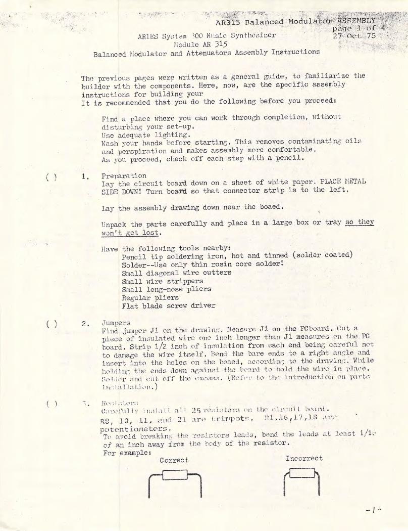
1 . P r e p a r a t i o nLay the circuit board down on a sheet of white paper. PLACE METALSIDE DOWN! Turn board, so that connector strip is to the left.
Lay the assembly drawing down near the boaed.
Unpack the parts carefully and place in a large box or tray so theywon't get lost.
Have the following tools nearby:Pencil tip soldering iron, hot and tinned (solder coated)Solder—Use only thin rosin core solder 1Small diagonal wire cuttersSmall wire strippersSmall lcng-nose pliersRegular pliersFlat blade screw driver
JumpersFind jumper Jl on the drawing. Measure J J. on the FCboard. Gut apiece of insulated wire one inch longer than Ji Measures en the PCboard. Strip l/2 inch of insulation from each end being careful notto damage the wire itself. Bend the bare ends to a right angle andinsert into the holes on the boaed, according to the drawing. Whileholding the ends down against the board to hold the wire in place.Poldfr and cut off the excess. (Refer to the introduction on ports1 n:".l al lalu.on.)
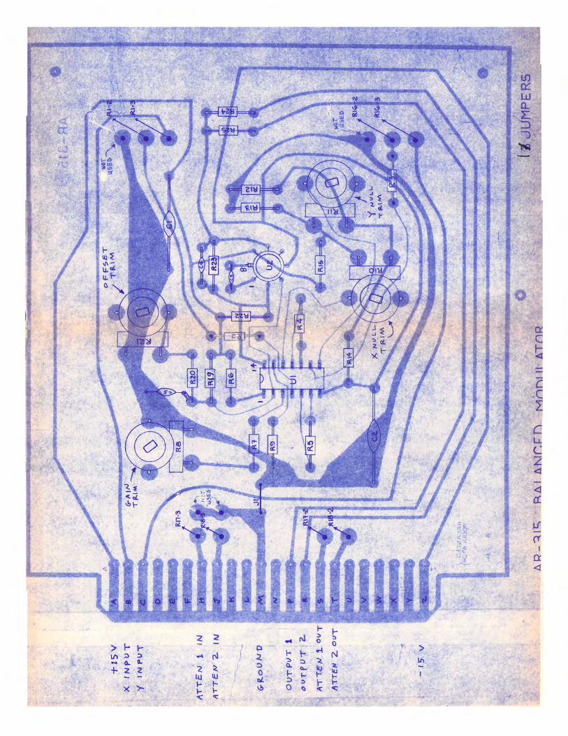
( 1 R e s i s t o r s .Carefully irista'.U n.i I 25 resistors on the nixvuil board.RS, 10 , 11 , and 21 a iv t r impot* : . B l ,16 ,17 ,18 ,nvp o t e n t i o m e t e r s . ,To avoid breaking the resistors leads, bend tne aeads at least i/itof an inch away from the body of the resistor.For example:
C o r r e c t I n c o r r e c t
r ^ i f =h
- /
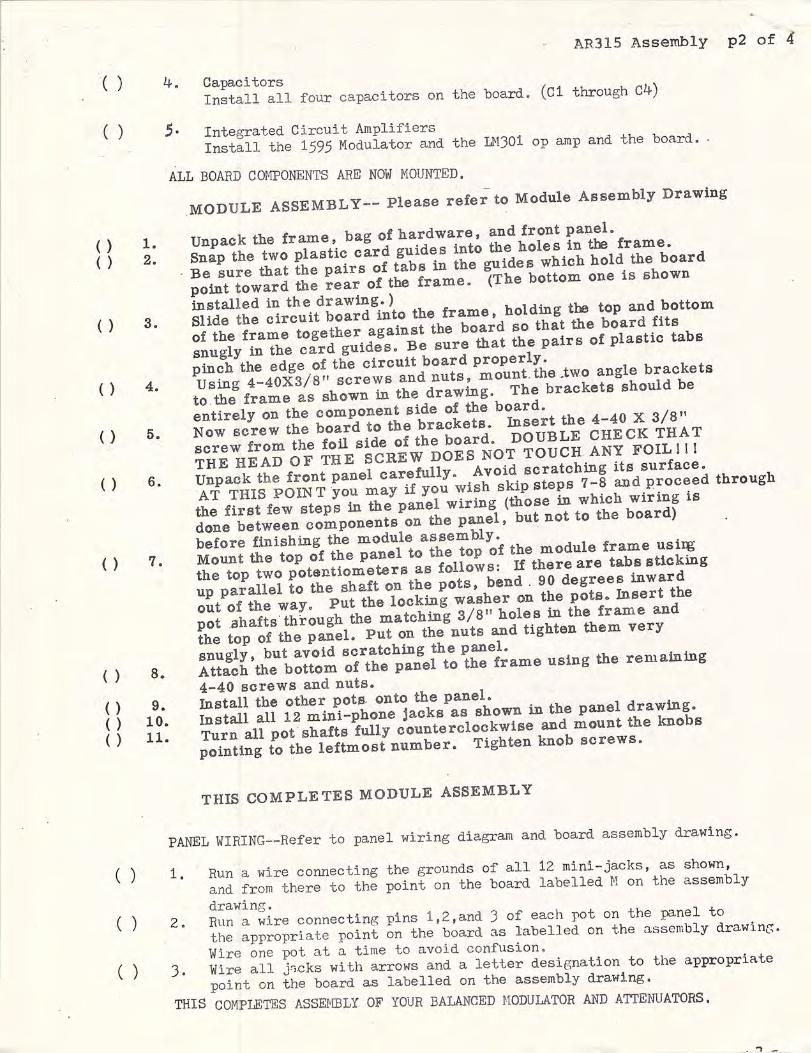
AR315 Assembly p2 of 4
( ) * * • • C a p a c i t o r s / • „ « . , u n MInstall all four capacitors on the board. (Cl through W)
( ) 5 - I n t e g r a t e d C i r c u i t A m p l i fi e r sInstall the 1595 Modulator and the LM301 op amp and the board. -
ALL BOARD COMPONENTS ARE NOW MOUNTED.
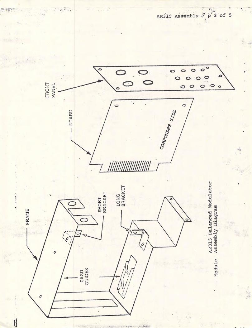
MODULE ASSEMBLY- Please refer to Module Assembly Drawing
( , l. Unpack the frame bag of hardware and front panel.i 2 . S n a p t h e t w o p l a s t i c c a r d g u i d e s i n t o m » • f t b d< ' B e s u r e t h a t t h e p a i r s o f t a b s■» M f c . $ £ • • * £ £ £ i s s h o w npoint toward the rear of the irame. (i"«i n s t a l l e d i n t h e d r a w i n g . ) h o l d i n g t h e t o p a n d b o t t o m
/ ) 3. Sl ide the circui t board into the »■£•»"; th£ ^ board f i ts( ' of the frame together against the board so^thataesnugly in the card guides. Be sure that the pairs oi piabpinch the edge of the circuit board properly.
( ) 4 . U s i n g 4 - 4 0 X 3 / 8 " s c r e w s « d » ^ » ^ e ^ r ^ V r t i a « l d b ew to the f rame as shown in the <drawing. ine
U A n T P f c 0 ^ y o r m : ^ ' - w ^ h ^ s " ° s h 7 - I a n d p r o c e e d t h r o u g h
± sssr£ p&d1 ' -s rL^ r the* i*fcl«.u Put the locking washer on the pots. Insert tne°o p;xiAT£&£ K*'lt%££%Zr.irT
the top of the panel. Put on the nuts and tighten them very
T ^ X Z l o f - ' e ^ e ' r t n e t a m e u s i n g t h e r e m a i n i n g
( ) 6 .
4-40 screws and nuts.( ) 8 .
( ) 9 .
< > " ' J S S [ S i V e T i l ^ ^ Z T ^ i e i k n o b s c r e w s .
THIS COMPLETES MODULE ASSEMBLY
4-4U screws auu u.u.*o*I n s t a l l t h e o t h e r p o t s - o n t o t h e p a n e l . d r a w i n g .
Turn all P™ sflf"» «,/T,„«1h«r. Tiehten knob screws.
PANEL WIRING—Refer to panel wiring diagram and board assembly drawing.
( ) 1 Run a wire connecting the grounds of all 12 mini-jacks as shown,U and from there to the point on the board labelled H on the assembly
( ) 2 RunTwire connecting pins 1,2,and 3 of each pot on the panel toU the appropriate point on the board as labelled on the assembly drawing,Wire one pot at a time to avoid confusion.
( ) 3 Wire all jacks with arrows and a letter designation to the appropriateV ' ' point on the board as labelled on the assembly drawing.
THIS COMPLETES ASSEMBLY OF YOUR BALANCED MODULATOR AND ATTENUATORS.
s« ^ap", j£„
AR315 Assembly 4' p* 3 of 5
t
I
MO+Jtod■O0E g
(CTS MCD (7*o (fl-d •H03 a
r - l(d > ie rH
IT) irH <ur o COPi W< <
0)r H3
T3os
• ,-*-■• i
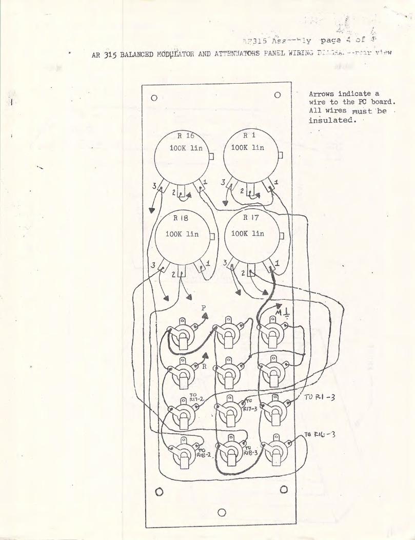
*P3i5'Ass—vly paga 4 of '$•AR 315 BALANCED MOPyikTOR AND ATTENUATORS PANEL WIRING DIAGr̂ —rear view
Arrows indicate awire to the PC board,All wires must bei n s u l a t e d .
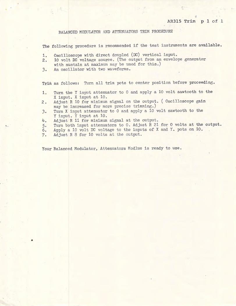
AR315 Trim p 1 of 1
BALANCED MODULATOR AND ATTENUATORS TRIM PROCEDURE
The following procedure is recommended if the test instruments are available.
1. Oscilloscope with direct doupled (DC) vertical input.2. 10 volt DC voltage source. (The output from an envelope generator
with sustain at maximum may be used for this.)3. An oscillator with two waveforms.
Trim as follows: Turn all trim pots to center position before proceeding.
1. Turn the Y input attenuator to 0 and apply a 10 volt sawtooth to theX input. X input at 10.
2. Adjust R 10 for minimum signal on the output. ( Oscilloscope gainmay be increased for more precise trimming.)
3. Turn X input attenuator to 0 and apply a 10 volt sawtooth to theY input. Y input at 10,
k. Adjust R 11 for minimum signal at the output.5. Turn both input attenuators to 0. Adjust R 21 for 0 volts at the output.6. Apply a 10 volt DC voltage to the inputs of X and Y. pots on 10.7. Adjust R 8 for 10 volts at the output.
Your Balanced Modulator, Attenuators Modlue is ready to use,
n f p
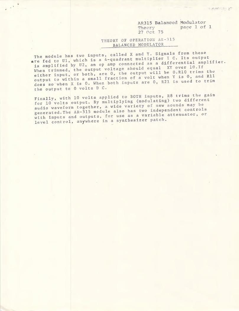
AR315 Balanced ModulatorT h e o r y p a g e 1 o f 127 Oct 7 5
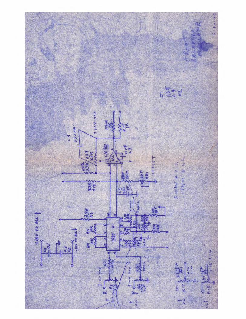
THEORY OF OPERATION AR-BALANCED MODULATOR
15
T h e m o d u l e h a s t w o i n p u t s , c a l l e d X a n d Y S i g n a l s f r o . t h e s e^ p * a r n T i l w h i c h i s a 4 - q u a d r a n t m u l t i p l i e r I C . i t s o u t p u t' a m l i ° f i e d ' k h u 2 ! a n o P a m p c o n n e c t e d a s a d i f f e r e n t i a l a m p l i f i e r
W h e n t r i m m e d , t h e o u t p u t v o l t a g e s h o u l d e q u a l X Y o v e r 1 0 I fe i t h e r i n p u t , o r b o t h , a r e 0 , t h e o u t p u t w i l l b e 0 . R I O t r i m s t h eo u t P u t t o w i t h i n a s m a l l f r a c t i o n o f a v o l t w h e n Y i s 0 a n d R l ldoes so when X i s 0 . When bo th i npu ts a re 0 , R21 i s used t o t r imt h e o u t p u t t o 0 v o l t s D C .
F i n a l l y , w i t h 1 0 v o l t s a p p l i e d t o B O T H i n p u t s , R 8 t r i m s t h e g a i nf o r 1 0 v o l t s o u t p u t . B y m u l t i p l y i n g ( m o d u l a t i n g ) t w o d i f f e r e n ta u d i o w a v e f o r m t o g e t h e r, a w i d e v a r i e t y o f n e w s o u n d s m a y b eg e n e r a t e d . T h e A R - 3 1 5 m o d u l e a l s o h a s t w o i n d e p e n d e n t c o n t r o l sw i t h i n p u t s a n d o u t p u t s , f o r u s e a s a v a r i a b l e a t t e n u a t o r , o rl e v e l c o n t r o l , a n y w h e r e i n a s y n t h e s i z e r p a t c h .