Embed Size (px)
Citation preview

IEEE TRANSACTIONS ON VLSI SYSTEMS, VOL. XX, NO. Y, MONTH 1995 1
Programmable Active Memories:Recon�gurable Systems Come of AgeJ. Vuillemin, P. Bertin, D. Roncin, M. Shand, H. Touati, P. Boucard
Abstract|Programmable Active Memories (PAM) are a novelform of universal recon�gurable hardware co-processor.Based on Field-Programmable Gate Array (FPGA) technology,a PAM is a virtual machine, controlled by a standard micro-processor, which can be dynamically and inde�nitely recon-�gured into a large number of application-speci�c circuits.PAMs o�er a new mixture of hardware performance andsoftware versatility.We review the important architectural features of PAMs,
through the example of DECPeRLe-1, an experimental de-vice built in 1992.PAM programming is presented, in contrast to classical
gate-array and full custom circuit design. Our emphasis ison large, code-generated synchronous systems descriptions;no compromise is made with regard to the performance ofthe target circuits.We exhibit a dozen applications where PAM technology
proves superior, both in performance and cost, to everyother existing technology, including supercomputers, mas-sively parallel machines, and conventional custom hardware.The �elds covered include computer arithmetic, cryptog-
raphy, error correction, image analysis, stereo vision, videocompression, sound synthesis, neural networks, high-energyphysics, thermodynamics, biology and astronomy.At comparable cost, the computing power virtually avail-
able in a PAM exceeds that of conventional processors bya factor 10 to 1000, depending on the speci�c application,in 1992. A technology shrink increases the performance gapbetween conventional processors and PAMs. By Noyce'slaw, we predict by how much the performance gap will widenwith time.
Keywords| Programmable Active Memory, PAM, recon-�gurable system, �eld-programmable gate array, FPGA.
I. Introduction
THERE are two ways to implement a speci�c high-speed digital processing task.
� The simplest is to program some general-purpose com-puter to perform the processing. In this software ap-proach, one e�ectively maps the algorithm of interestonto a �xed machine architecture. However, the struc-ture of that machine will have been highly optimizedto process arbitrary code. In many cases, it will bepoorly suited to the speci�c algorithm, so performancewill be short of the required speed.
� The alternative is to design ad hoc circuitry forthe speci�c algorithm. In this hardware ap-proach, the machine structure|processors, storageand interconnect|is tailored to the application. Theresult is more e�cient, with less actual circuitry thangeneral-purpose computers require.
This work was done at Digital Equipment Corporation's Paris Re-search Laboratory (DEC-PRL, 92500 Rueil-Malmaison, France) from1988 to 1994. J. Vuillemin, D. Roncin, M. Shand, H. Touati andP. Boucard were members of PRL research sta�. P. Bertin was a vis-iting scientist from Institut National de Recherche en Informatiqueet en Automatique (INRIA, 78150 Rocquencourt, France).
The disadvantage of the hardware approach is that aspeci�c architecture is usually limited to processing a smallnumber of algorithms, often a single one. Meanwhile, thegeneral-purpose computer can be programmed to processevery computable function, as we have known since thedays of Church and Turing.
Adding special-purpose hardware to a universal machine,say for video compression, speeds up the processor|whenthe system is actually compressing video. It contributesnothing when the system is required to perform some dif-ferent task, say cryptography or stereo vision.
We present an alternative machine architecture thato�ers the best of both worlds: software versatility andhardware performance. The proposal is a standardhigh-performance microprocessor enhanced by a PAM co-processor. The PAM can be con�gured as a wide class ofspeci�c hardware systems, one for each interesting applica-tion. PAMs merge together hardware and software.
This paper presents results from seven years of research,at INRIA, DEC-PRL and other places. It addresses thefollowing topics:
How to build PAMs.How to program PAMs.What are the applications?
Section II introduces the principles of the underlyingFPGA technology.
Section III highlights the interesting features of PAMarchitecture.
Section IV presents some of the methods used in pro-gramming large PAM designs.
Section V describes a dozen applications, chosen from awide variety of scienti�c �elds. For each, PAM outperformsall other existing technologies. A hypothetical machineequipped with a dozen di�erent conventional co-processorswould achieve the same level of performance|at a higherprice. Through recon�guration, a PAM is able to time-share its internal circuitry between our twelve (or more)applications; the hypothetical machine would require dif-ferent custom circuits for each, that must be physicallypresent at all times.
We assess, in Section VI, the computing power of PAMtechnology, today and in the future.
II. Virtual circuits
The �rst commercial FPGA was introduced in 1986 byXilinx [1]. This revolutionary component has a large inter-nal con�guration memory, and two modes of operation: indownload mode, the con�guration memory can be written,as a whole, through some external device; once in con-

2 IEEE TRANSACTIONS ON VLSI SYSTEMS, VOL. XX, NO. Y, MONTH 1995
�gured mode a FPGA behaves like a regular application-speci�c integrated circuit (ASIC).To realize a FPGA, one simply connects together in a
regular mesh, n � m identical programmmable active bits(PABs). Surprisingly enough, there are many ways to im-plement a PAB with the required universality. In partic-ular, it can be built from either or both of the followingprimitives:
� a con�gurable logic block implements a boolean func-tion with k inputs (typically 2 � k � 6); its truth tableis de�ned by 2k (or less) con�guration bits, stored inlocal registers;
� a con�gurable routing block implements a switchboxwhose connectivity table is set by local con�gurationbits.
Such a FPGA implements a Von Neumann cellular automa-ton. What is more, the FPGA is a universal example ofsuch a structure: any synchronous digital circuit can be em-ulated, through a suitable con�guration, on a large enoughFPGA, for a slow enough clock.Some vendors, such as Xilinx [2] or AT&T [3], form
their PABs from both con�gurable routing and logic blocks.Other early ones, such as Algotronix [4] (now with Xilinx)or Concurrent Logic [5] (now with Atmel), combine rout-ing and computing functions into a single primitive|thisis the �ne grain approach. An idealized implementation ofthis �ne grain concept is given in �gure 1. A third possi-bility is to build the PAB from a con�gurable routing boxconnected to a �xed (non con�gurable) universal gate suchas a nor or a multiplexor [6].
NSEW
nsew
r R
clk
n N
S
E
W
w
e
s
This PAB has 4 inputs hn; s; e;wi, 4 outputshN;S;E;W i, one register ( ip- op) with input R and out-put r, and a combinational gate
g(n; s; e;w; r) = (N;S;E;W;R)
The truth table of g is speci�ed by 160 = 5� 32 bits.
Fig. 1. Field-programmable gate array
Each FPGA implementation can emulate each of theothers, granted enough PABs. In order to make quanti-tative performance comparisons between the diverse sig-ni�cant implementations, let us, from now on, choose asour reference unit any active bit with one 4-input booleanfunction|con�gurable or not|and one internal bit of state(see section VI and Vuillemin [7]). With its �ve 5-inputfunctions, the PAB from �gure 1 counts for ten or so suchunits.
The FPGA is a virtual circuit which can behave like anumber of di�erent ASICs: all it takes to emulate a par-ticular one is to feed the proper con�guration bits. Thismeans that prototypes can be made quickly, tested andcorrected. The development cycle of circuits with FPGAtechnology is typically measured in weeks, as opposed tomonths for hardwired gate array techniques. But FPGAsare used not just for prototypes; they also get incorporatedin many production units. In all branches of the electronicsindustry other than the mass market, the use of FPGAs isexpanding, despite the fact that they still cost ten timesas much as ASICs in volume production. In 1992, FPGAswere the fastest growing part of the semi-conductor indus-try, increasing output by 40 %, compared with 10 % forchips overall.As a consequence, FPGAs are on the leading edge of
silicon chips. They grow bigger and faster at the rate oftheir enabling technology, namely that of the static RAMused for storing the internal con�guration.In the past 40 years, the feature size of silicon technol-
ogy has been shrinking by a factor 1=� � 1:25 each year.This phenomenon is known as Noyce's thesis; it was �rstobserved in the early sixties. The implications of Noyce'sthesis for FPGA technology are analyzed by Vuillemin [7].The prediction is that the leading edge FPGA, which has400 PABs operating at 25 MHz in 1992, will, by year 2001,contain 25k PABs operating at 200 MHz.
III. PAMs as Virtual Machines
The purpose of a PAM is to implement a virtual machinethat can be dynamically con�gured as a large number ofspeci�c hardware devices.
FPGAarray
Local RAM
Hos
tco
mpu
ter
in
out in’
out’
Externaldevices
download
Fig. 2. Programmable Active Memory
The structure of a generic PAM is found in �gure 2. Itis connected|through the in and out links|to a host pro-cessor. A function of the host is to download con�gurationbitstreams into the PAM. After con�guration, the PAMbehaves, electrically and logically, like the ASIC de�ned bythe speci�c bitstream. It may operate in stand-alone mode,hooked to some external system|through the in0 and out0
links. It may operate as a co-processor under host control,specialized to speed-up some crucial computation. It mayoperate as both, and connect the host to some externalsystem, like an audio or video device, or some other PAM.To justify our choice of name, observe that a PAM is
attached to some high-speed bus of the host computer,like any RAM memory module. The processor can write
VUILLEMIN ET AL.: PROGRAMMABLE ACTIVE MEMORIES, RECONFIGURABLE SYSTEMS COME OF AGE 3
adrN
adrE
adrS
adrW
adrS
adrN
adrW
adrE
M M M M
M M M M
M M M M
M M M M
C
C
S
S
S
S
S
R
R
R
R
>>
<<
FIFOs
Hostadapter
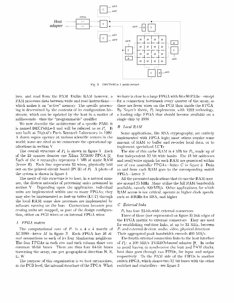
Fig. 3. DECPeRLe-1 architecture
into, and read from the PAM. Unlike RAM however, aPAM processes data between write and read instructions|which makes it an \active" memory. The speci�c process-ing is determined by the contents of its con�guration bit-stream, which can be updated by the host in a matter ofmilliseconds|thus the \programmable" quali�er.We now describe the architecture of a speci�c PAM: it
is named DECPeRLe-1 and will be referred to as P1. Itwas built at Digital's Paris Research Laboratory in 1992.A dozen copies operate at various scienti�c centers in theworld; some are cited as we enumerate the operational ap-plications in section V.The overall structure of P1 is shown in �gure 3. Each
of the 23 squares denotes one Xilinx XC3090 FPGA [2].Each of the 4 rectangles represents 1 MB of static RAM(letter R). Each line represents 32 wires, physically laidout on the printed circuit board (PCB) of P1. A photo ofthe system is shown in �gure 4.The merit of this structure is to host, in a natural man-
ner, the diverse networks of processing units presented insection V. Depending upon the application, individualunits are implemented within one to many FPGAs; theymay also be implemented as look-up tables (LUT) throughthe local RAM; some slow processes are implemented bysoftware running on the host. Connections between pro-cessing units are mapped, as part of the design con�gura-tion, either on PCB wires or on internal FPGA wires.
A. FPGA matrix
The computational core of P1 is a 4 � 4 matrix ofXC3090|letter M in �gure 3. Each FPGA has 16 di-rect connections to each of its four Manhattan neighbors.The four FPGAs in each row and each column share twocommon 16-bit buses. There are thus four 64-bit busestraversing the array, one per geographical direction N, S,E, W.The purpose of this organization is to best extrapolate,
at the PCB level, the internal structure of the FPGA. What
we have is close to a large FPGAwith 64�80 PABs|exceptfor a connection bottleneck every quarter of the array, asthere are fewer wires on the PCB than inside the FPGA.By Noyce's thesis, P1 implements, with 1992 technology,a leading edge FPGA that should become available on asingle chip by 1998.
B. Local RAM
Some applications, like RSA cryptography, are entirelyimplemented with FPGA logic; most others require someamount of RAM to bu�er and re-order local data, or toimplement specialized LUTs.The size of this cache RAM is 4 MB for P1, made up of
four independent 32-bit-wide banks. The 18-bit addressesand read/write signals for each RAM are generated withinone of two controller FPGAs|letter C in �gure 3. Datato and from each RAM goes to the corresponding switchFPGA|letter S.All the presented applications that do use the RAM oper-
ate around 25 MHz. Many utilize the full RAM bandwidthavailable, namely 400 MB/s. Other applications, for whichRAM access is not critical, operate at higher clock speeds,such as 40MHz for RSA, and higher.
C. External links
P1 has four 32-bit-wide external connectors.Three of these (not represented on �gure 3) link edges of
the FPGA matrix to external connectors. They are usedfor establishing real-time links, at up to 33 MHz, betweenP1 and external devices: audio, video, physical detectors. . .Their aggregated peak bandwidth exceeds 400 MB/s.The fourth external connection links to the host interface
of P1: a 100 MB/s TURBOchannel adapter [8]. In orderto avoid having to synchronize the host and PAM clocks,host data goes through two FIFOs, for input and outputrespectively. To the PAM side of the FIFOs is anotherswitch FPGA, which shares two 32-bit buses with the otherswitches and controllers|see �gure 3.

4 IEEE TRANSACTIONS ON VLSI SYSTEMS, VOL. XX, NO. Y, MONTH 1995
Fig. 4. DECPeRLe-1 and its TURBOchannel interface board
The host connection itself consists of a host-independentpart implemented on the P1 mother board and a host-dependent part implemented on a small option board spe-ci�c to the host bus. A short cable links the two parts|see�gure 4.In addition to the above, P1 features daughter-board
connectors that can provide more than 1.2 GB/s of band-width to specialized hardware extensions.
D. Firmware
One extra FPGA on P1 is not con�gurable by the user;call it POM, by analogy with ROM. Its function is to pro-vide control over the state of the PAM, through softwarefrom the host.The logical protocol of the host bus itself is programmed
in POM con�guration. Adapting from TURBOchannel tosome other logical bus format, such as VME, HIPPI orPCI is just a matter of re-programming the POM and re-designing the small host-dependent interface board.A function of the POM is to assist the host in download-
ing a PAM con�guration|1.5 Mb for P1. Thanks to thishardware assist, we are able to recon�gure P1 up to �ftytimes per second, a crucial feature in some applications.
One can regard P1 as a software silicon foundry, with a20 ms turn-around time.
We take advantage of an extra feature of the XC3090component: it is possible to dynamically read back the con-tents of the internal state register of each PAB. Togetherwith a clock stepping facility|stop the main clock and trig-ger clock cycles one at a time from the host|this providesa powerful debugging tool, where one takes a snapshot ofthe complete internal state of the system after each clockcycle. This feature drastically reduces the need for softwaresimulation of our designs.
PAM designs are synchronous circuits: all registers areupdated on each cycle of the same global clock. The maxi-mum speed of a design is directly determined by its criticalcombinational path. This varies from one PAM design toanother. It has thus been necessary to design a clock dis-tribution system whose speed can be programmed as partof the design con�guration. On P1, the clock can be �nelytuned, with increments on the order of 0.01%, for frequen-cies up to 100 MHz.
A typical P1 design receives a logically uninterrupted ow of data, through the input FIFO. It performs someprocessing, and delivers its results, in the same manner,

VUILLEMIN ET AL.: PROGRAMMABLE ACTIVE MEMORIES, RECONFIGURABLE SYSTEMS COME OF AGE 5
through the output FIFO. The host is responsible for�lling-in and emptying-out the other side of both FIFOs.Our �rmware supports a mode in which the applicationclock automatically stops when P1 attempts to read anempty FIFO or write a full one, e�ectively providing fullyautomatic and transparent ow-control.The full �rmware functionality may be controlled
through host software. Most of it is also available to thehardware design: all relevant wires are brought to the twocontroller FPGAs of P1. This allows a design to synchro-nize itself, in the same manner, with some of the externallinks. Another unique possibility is the dynamic tuningof the clock. This feature is used in designs where a slowand infrequent operation|say changing the value of someglobal controls every 256 cycles|coexists with fast and fre-quent operations. The strategy is then to slow the clockdown before the infrequent operation|every 256 cycles|and speed it up afterwards|for 255 cycles. Tricky, butdoable.
E. Other Recon�gurable Systems
Besides our PAMs, which were built �rst at INRIA in1987 up to Perle-0, whose architecture is described in somedetail in an earlier report [9], then at DEC-PRL, othersuccessful implementations of recon�gurable systems havebeen reported, in particular at the universities of Edin-burgh [10] and Zurich [11], and at the Supercomputer Re-search Center in Maryland [12].The ENABLE machine is a system, built from FPGAs
and SRAM, speci�cally constructed at the university ofMannheim [13] for solving the TRT problem of section V-G.2. Many similar application-speci�c machines have beenbuilt in the recent years: their recon�gurable nature is ex-ploited only while developing and debugging the applica-tion. Once complete, the �nal con�guration is frozen, onceand for all|until the next \hardware release".Commercial products already exist: QuickTurn [14] sells
large con�gurable systems, dedicated to hardware emula-tion. Compugen [15] sells a modular PAM-like hardware,together with several con�gurations focusing on geneticmatching algorithms. More systems exist than just theones mentioned here.A thorough presentation of the issues involved in PAM
design, with alternative implementation choices, is givenby Bertin [16].
IV. PAM programming
A PAM program consists of three parts:1. The driving software, which runs on the host and con-trols the PAM hardware.
2. The logic equations describing the synchronous hard-ware implemented on the PAM board.
3. The placement and routing directives that guide theimplementation of the logic equations onto the PAMboard.
The driving software is written in C or C++ and is linkedto a runtime library encapsulating a device driver. Thelogic equations and the placement and routing directives
are generated algorithmically by a C++ program. As a de-liberate choice of methodology, all PAM design circuits aredigital and synchronous. Asynchronous features|such asRAM write pulses, FIFO ags decoding or clock tuning|are pushed into the �rmware (POM) where they get imple-mented once and for all.A full P1 design is a large piece of hardware: excluding
the RAM, twenty-three XC3090 containing 15k PABs areroughly the equivalent of 200k gates. This amount of logicwould barely �t in the largest gate arrays available in 1994.The goal of a P1 designer is to encode, through a 1.5 Mb
bitstream, the logic equations, the placement and the rout-ing of �fteen thousand PABs in order to meet the per-formance requirements of a compute-intensive task. Toachieve this goal with a reasonable degree of e�ciency, adesigner needs full control over the �nal logic implementa-tion and layout. In 1992, no existing computer-aided design(CAD) tool was adapted to such needs.Emerging synthesis tools were too wasteful in circuit area
and delay. One has to keep in mind that we already pay aperformance penalty by using SRAM-based FPGAs insteadof raw silicon. Complex designs can be synthesized, placedand routed automatically only when they do not attemptto reach high device utilization; even then, the resultingcircuitry is signi�cantly slower than what can be achievedby careful hand placement.Careful low-level circuit implementation has always been
possible through a painful and laborious process: schematiccapture. For PAM programming, schematic capture is nota viable alternative: it can provide the best performance,but it is too labor intensive for large designs.Given these constraints, we have but one choice: a
middle-ground approach where designs are described algo-rithmically at the structural level, and the structure can beannotated with geometry and routing information to helpgenerate the �nal physical design.
A. Programming tools
We �rst had to choose a programming language to de-scribe circuits. Three choices were possible: a general-purpose programming language such as C++, a hardwaredescription language such as VHDL, or our own language.We do not discuss the latter approach here; it is the subjectof current research.We decided to use C++ for reasons of economy and sim-
plicity. VHDL is a complex, expensive language. C++programming environments are considerably cheaper, andwe are tapping a much wider market in terms of training,documentation and programming tools. Though we had todevelop a generic software library to handle netlist gener-ation and simulation, the amount of work remains limited.Moreover, we keep full control over the generated netlist,and we can include circuit geometry information as desired.
A.1 The netlist library
To describe synchronous circuits with our C++ libraryis straightforward. We introduce a new type Net, overloadthe boolean operators to describe combinational logic, and

6 IEEE TRANSACTIONS ON VLSI SYSTEMS, VOL. XX, NO. Y, MONTH 1995
add a primitive for the synchronous register. From these, aC++ program can be written which generates a netlist rep-resenting any synchronous circuit. This type of low-leveldescription is made convenient by the use of basic program-ming techniques such as arrays, for loops, procedures anddata abstraction. Figure 5 shows, for example, a piece ofcode representing a generic n-bit ripple-carry adder.
template<int N>
struct RippleAdder: Block {
RippleAdder(): Block("RippleAdder"){}
void logic(Net<N>& a, Net<N>& b, Net<N>& c,
Net<N>& sum, Net& carry) {
input(a); input(b); input(c);
output(sum); output(carry);
for (int i = 0; i < N; i++){
sum[i] = a[i] ^ b[i] ^ c[i];
carry[i] = (a[i] & b[i])
| (b[i] & c[i])
| (c[i] & a[i]);
}
}
};
Fig. 5. Circuit description in C++
The execution of such a program builds a netlist in mem-ory; this netlist can be analyzed and translated into anappropriate format (XNF or EDIF), or used directly forsimulation. Linking a netlist description program with be-havioral code yields mixed-mode simulation with no speciale�ort.
Since we have direct access to the netlist at this level ofdescription, we can easily annotate logic operators withplacement directives. For example, to specify that ourripple-carry adder should be aligned vertically, with thepaired carry and sum bits generated by the same logicblock, we simply add the lines shown in �gure 6 to thedescription of the adder.
void placement(Net<N>& sum, Net<N>& carry) {
for (int i = 0; i < N; i++) {
carry[i] <<= sum[i];
sum[i+1] <<= sum[i] + OFFSET(0,1);
}
Fig. 6. Circuit layout in C++
Contrary to the silicon compilers from a decade ago[17], these placement annotations do not a�ect the logicbehavior of the generated netlist. They do not specifycontacts; they only specify the partitioning of logic intophysical blocks and the absolute or relative placement ofthese blocks in a two-dimensional grid. A back-end toolanalyzes these attributes and emulates the interface of aschematic capture software in order to guarantee that the
placement and logic partitioning information is preservedby the FPGA vendor software.
A.2 The runtime library
At the system level, the programming environment pro-vides two main functions: a device driver interface, and fullsimulation support of that interface. This simulation capa-bility allows the designer to operate together the hardwareand software parts from a PAM program. The device driverinterface provides the mandatory controls to the applica-tion program: the usual UNIX I/O interface with open,close, synchronous and asynchronous read and write; down-load of the con�guration bitstreams for the PAM FPGAs;readback of their state (i.e. the values of all PAB registers);read and write of the PAM static RAMs; software controlof the PAM board clock.
A.3 Lessons
The main lesson we draw from our experience with theseprogramming tools is that PAM programming is much eas-ier than ASIC development. Students with no electricalengineering background were able to use our tools aftera few weeks of training. In particular, users can easilydevelop their own module generators in matters of days,while only highly skilled engineers are able to write mod-ule generators for custom VLSI. This capability is one ofthe main reasons why we were able to develop such complexapplications spanning dozens of chips, with engineers andstudents not previously exposed to PAM, each in a matterof months.
B. Debugging and optimization tools
Debugging of a PAM design can be done entirely throughsoftware. Mixed-mode simulation at the block level al-lows designers to certify datapath components before us-ing them in complex designs. Full-system simulation elim-inates the need for generating special input patterns totest the hardware part of the program. Full-system simu-lation allows for hardware/software codebug: both applica-tion driver and hardware, working together.
After simple bugs have been removed, it becomes nec-essary to simulate the design on a large number of cycles.To do so, the most e�ective technique is to compile thedesign into a bitstream, download this bitstream into theboard, and run the board in trace mode (single-step theclock, readback the board state at each cycle and collectthese states for analysis; it is possible to run this modeat up to 100 Hz). In simple cases, this can be done withno modi�cation to the runtime application source code.In complex cases, all necessary primitives are available tobuild application-speci�c code to generate and/or analyzethe readback traces.
P1's clock generator can also be operated in double-stepmode. In that mode, the clock runs at full speed ev-ery second cycle. By comparing double-step traces takenat increasing clock frequencies with a previously recordedsingle-step trace, we can automatically locate the critical

VUILLEMIN ET AL.: PROGRAMMABLE ACTIVE MEMORIES, RECONFIGURABLE SYSTEMS COME OF AGE 7
path of a design for a given execution. This method allevi-ates the need to rely on delay simulation as provided by thestandard industrial simulation packages. It is necessary toperform that tedious task only once, when certifying theoperating speed of the �nal design.We developed a screen visualization tool called showRB
to help analyze readback traces. It can display the stateof every ip- op in every FPGA of a PAM board, at therate of tens of frames per second. In conjunction with thedouble-step mode, it can be used to detect critical pathsalong execution traces. Interestingly enough, such a toolalso proved invaluable in demonstrating the structure ofsome hardware algorithms.
V. Applications
Our applications were chosen to span a wide range of cur-rent leading-edge computational challenges. In each case,we provide a brief description of the design, a performancecomparison with similar reported work, and pointers topublications describing the work in more detail.One paradigm was systematically applied:
Cast the inner loop in PAM hardware; let softwarehandle the rest!
In what follows, a� b denotes the quotient and a �j� b theremainder in the euclidean integer division of a by b.
A. Long integer arithmetic
A reg.
P s/p reg.HostData
32512 / 2k x Mult. Slice
32
2
2
2
2
HostAddr.
A p/s reg.
B p/s reg.
S p/s reg.
Cntr.
Fig. 7. Long multiplication
PAMs may be con�gured as long integer multipliers [18].They compute the product
P = A�B + S
where A is an n-bit long multiplier, and B;S are arbitrarysize multiplicands and summands [19]; n may be up to 2kfor the P1 implementation.Our multipliers are interfaced with the public domain
arbitrary-precision arithmetic package BigNum [20]: pro-grams based on that software automatically bene�t fromthe PAM, by simply linking with an appropriatedly modi-�ed BigNum library.P1 computes product bits at 66 Mb/s (using radix 4 op-
erations at 33 MHz), which is faster than all previouslypublished benchmarks. This is 16 times over the �guresreported by Buell and Ward [21] for the Cray II and Cy-ber 170/750. P1's multiplier can compute a 50-coe�cient
16-bit polynomial convolution (FIR �lter) at 16 times au-dio real time (2� 24-bit samples at 48 kHz).
The �rst operational version of this multiplier was devel-oped in less than a week. Two subsequent versions, whichre�ned the design on the basis of actual performance mea-surements, were each developed in less than 5 man-days.
A more aggressive multiplier design is reported by Louieand Ercegovac [22]: using radix 16 and deep pipeline, thismultiplier operates at 79 MHz, which is 2.5 faster thanours within 3 times the area. At that speed, this design isfaster than conventional multipliers, even for short 32-bitoperands.
B. RSA cryptography
To investigate further the tradeo�s in our hybrid hard-ware and software system, we have focused on the RSAcryptosystem [23]. Both encryption and decryption involvecomputing modular exponentials, which can be decom-posed as sequences of long modular multiplications, withoperand sizes ranging from 256 bits to 1k bits.
Starting from the general-purpose multiplier above, wehave implemented a series of systems spanning two ordersof magnitude in performance, over three years.
Our �rst system [18] uses three di�erently programmedPerle-0 boards, all operating in parallel with the host. At200 kb/s decoding speed, this was faster than all existing512-bit RSA implementations, regardless of technology, in1990. A survey by E. Brickell [24] grants the previous speedrecord for 512-bit key RSA decryption to an ASIC fromAT&T, at 19 kb/s.
2
B1
B2
S
2
M
+
X
X
256
32
32
Data In
Data Out
Fig. 8. RSA cryptography
Table I recalls the various original hardware algorithmsused in our latest implementation of RSA, and quanti�eseach speedup achieved.
TABLE I
RSA speedup techniques
Algorithm SpeedupChinese remainders 4Precompute powers 1:25Hensel's division 1:5Carry completion � 2Quotient pipelining 4

8 IEEE TRANSACTIONS ON VLSI SYSTEMS, VOL. XX, NO. Y, MONTH 1995
The resulting P1 design for RSA cryptography combinesall of the techniques above (see Shand and Vuillemin [25]for details). To fully exploit the available logic gates theP1 design operates with 970-bit keys. At this key length itdelivers an RSA secret decryption rate of 185 kb/s. Thisis an order of magnitude faster than any previously re-ported running implementation. For 512-bit keys the samedatapath delivers a decryption rate in excess of 300 kb/salthough it uses only half the logic resources in P1.PAM implementations of RSA rely on recon�gurability
in many ways: we use a di�erent PAM design for RSAencryption and decryption; we generate a di�erent hard-ware modular multiplier for each di�erent prime moduluswith the coe�cients of the binary representation of eachmodulus hardwired into the logic equations of the design.
C. Molecular biology
Given an alphabet A = (a1; : : : ; an), a probability(Sij)i;j=1:::n of substitution of ai by aj , and a probability(Ii)i=1:::n (resp. (Di)i=1:::n) of insertion (resp. deletion)of ai, one can use a classical dynamic programming algo-rithm to compute the probability of transforming a wordw1 over A into another one w2; this de�nes a distance be-tween words in A.
30k−word dictionary
Coefficients
P1 P2 P3 P4 P5 Distance out
Char. in
Fig. 9. String matching
Applications include automated mail sorting throughOCR scanners, on-the- y keyboard spelling corrections,and DNA sequencing in biology.D. Lavenier from IRISA (Rennes, France) has imple-
mented this algorithm with a Perle-0 design which com-putes the distance between an input word and all 30k wordsin a dictionary; it reports the k words found in the dictio-nary which are closest to the input. The system processes200k words/s which is faster than a solution previously im-plemented at CNET using 12 Transputers. It has only halfof the performance obtained by a system previously devel-oped at IRISA based on 28 custom VLSI chips and twoprinted-circuit boards.The DNA matching algorithm [26] is one of the driving
applications for the PAM developed at the Supercomput-ing Research Center in Maryland [12]: the reported per-formance is, here again, in excess of that obtained withexisting supercomputers.The Compugen commercial company [15] sells the Bioc-
celerator, a PAM which can be con�gured as a number ofmolecular biology search functions. This device is a co-processor to a host server; it can be accessed through re-mote procedure call from any workstation on the network.
It is interfaced with a widely used software package and itsuse is transparent, except for the speed-up advantages.
D. Heat and Laplace equations
Solving the heat and Laplace equations has numerous ap-plications in mechanics, integrated circuit technology, uiddynamics, electrostatics, optics and �nance [27].The classical �nite di�erence method [28] provides com-
putational solutions to the heat and Laplace equations.Vuillemin [29] shows how to speed-up this computationwith help from special-purpose hardware. A �rst imple-mentation of the method on P1, by Vuillemin and Ro-cheteau [29], operates with a pipeline depth of 128 opera-
tors. Each operator computes T+T 0
2, where T and T 0 are
24-bit temperatures.
RA
M
RA
M...
Fig. 10. Heat and Laplace equations
At 20 MHz, this �rst design processes 5G operations|add and shift|per second. For such a smooth problem, onecan easily show [29] that �xed-point yields the same resultsas oating-point operations. The performance achieved bythis �rst 24-bit P1 design thus exceeds those reported byMcBryan et al. [30] [31], for solving the same problemswith the help of supercomputers. A sequential computermust execute 20 billion instructions per second in order toreproduce the same computation.S. Hadinger and P. Raynaud-Richard further improved
the implementation [32]. Re�ning the statistical analysis,they show that the datapath width can be reduced to 16bits provided the rounding-o� of the low-order bit is donerandomly|with all deterministic round-o� schemes, para-sitic stable solutions exist which signi�cantly perturb theresult. Their implementation therefore uses a 64-bit linearfeedback shift-register to randomly set the rounding direc-tion for each processing stage.The width reduction in the datapath allows us to extend
the pipeline length to 256, pushing the equivalent process-ing power up to 39 GIPS. Using P1's fast DMA-based I/Ocapabilities and a large bu�er of host memory, this designcan accurately simulate the evolution of temperature overtime in a 3-D volume, discretized on 5123 points, with arbi-trary power source distributions on the boundaries. It alsosupports the use of multigrid simulation, where one \zoomsout" to coarser discretization grids in order to rapidly ad-vance in simulated time, then \zooms back in" to full reso-lution, in order to accurately smooth out the desired �nalresult.
E. Neural networks
M. Skubiszewski [33] [34] has implemented a hardwareemulator for binary neural networks, based on the Boltz-mann machine model.The Boltzmann machine is a probabilistic algorithm
which minimizes quadratic forms over binary variables, i.e.

VUILLEMIN ET AL.: PROGRAMMABLE ACTIVE MEMORIES, RECONFIGURABLE SYSTEMS COME OF AGE 9
expressions of the form
E( ~N ) =n�1X
i=0
iX
j=0
wi;jNiNj
where ~N = (N0; : : : ; Nn�1) is a vector of binary variablesand (wi;j)0�i;j<n is a �xed matrix of weights. It is typicallyused to �nd approximate solutions to some NP-hard prob-lems, such as graph partitioning and circuit placement.
...
...
Proc# 1
Proc# 2
Proc# 32
Weight RAM
DataRAM
Host I/O
Fig. 11. Boltzmann machine
The latest P1 realization solves problems with 1400 bi-nary variables, using 16-bit weights, for a total computingpower of 500 megasynapses per second. (The megasynapseis the traditional unit used in this �eld; it amounts to onemillion additions and multiplications by small coe�cients.)
F. Multi-standard video compression
In view of the required input bandwidth (30 MB/s forstandard TV color images) and the amount of computationrequired by current standards (resp. 3, 4 and 8 Gop/s1 forJPEG, DCT3Dand MPEG), custom hardware is currentlynecessary for compressing video in real time.Matters get complicated, as several di�erent video com-
pression standards are emerging. The following showshow a single con�gurable system such as P1 can perform,through di�erent designs, three (or more) of the currentleading standards.JPEG The computation speci�ed by the Joint Photo-graphic Expert Group is performed in three stages, ac-cording to:
SourceImage
7! R 7! DCT 2 7! Q 7! A=HC 7!Compressed
Image
The initial RAM R is used to store 8 consecutive linesin the input image, with double bu�ering. It feeds theDCT 2 module with 8� 8 square sub-images.1. The two-dimensional DCT 2 (Discrete Cosine Trans-
form) maps 8� 8 squares from the space to the fre-quency domain.
2. Each frequency coe�cient is divided by a numberQ = Qx;y. The choice of the quantization table Qprovides a way to control the compromise between
1109 16-bit integer operations per second
the compression factor and the quality of the de-compressed image.
3. Run-length, and arithmetic or Hu�man encodingsA=HC are performed on the quantized values.
MPEG The Motion Picture Expert Group system doesmotion compensation (MC) by computing a correla-tion between blocks within two time-consecutive im-ages. The result is di�erence-coded, then goes througha processing similar to JPEG.
DigitalVideo
7! R 7! MC 7! �Code 7!Compressed
Video
MPEG-1 requires storage for only 4 images, after al-lowing for double bu�ering. The decoder is much sim-pler than the encoder, however, the MPEG decoderstill requires about as much hardware as the followingDCT3D .A detailed FPGA mapping of the motion estimationalgorithm|the core of the MPEG standard|is givenby Furtek [35]. Mapping this fully laid-out design ontoP1 would be a straightforward task.
DCT3D J. Vuillemin, D. Martineau, and J. Barraquandfrom PRL have used P1 to experiment with DCT
3D , a3-D version of JPEG|the third dimension being time.Except for RAM, this method requires only half asmuch hardware as MPEG. It leads to an excellentcompression factor, with an appropriate choice of thequantization table Q = Q(x; y; t), a 512-entry cube.Early experiments indicate that, for a given compres-sion rate, the quality of the restituted video is (sub-jectively) better with DCT3Dthan with MPEG.The method performs the following sequence of com-putations:
DigitalVideo
307! R
307! DCT 3 60
7! A=HC�27!
CompressedVideo
In this diagram, the numbers on the arrows indicatethe transfer bandwidth, in MB/s.
� The algorithm needs a video bu�er big enough tostore 8 consecutive images (twice for double bu�er-ing). Thus, DCT3Drequires 4 times more RAM thanMPEG.
� Past the initial video bu�er, all the processing isperformed in a straight pipeline operating on videocubes of size 83 � 16b, made of eight 8 � 8 squaresconsecutive in time.
This P1 design computes 48 �xed-point operations(32-bit outputs add, subtract, multiply and shift) at25 MHz, for a total of 1.4G operations per second.Based on our speci�cation software, we rate this al-gorithm, which requires a lot of data movement, at15 GIPS.

10 IEEE TRANSACTIONS ON VLSI SYSTEMS, VOL. XX, NO. Y, MONTH 1995
G. High-energy physics
G.1 Image classi�cation
The calorimeter is part of a series of benchmarks pro-posed by CERN2 [36]. The goal is to measure the per-formance of various computer architectures, in order tobuild the electronics required for the Large Hadron Collider(LHC), before the turn of the millennium. The calorime-ter is challenging, and well documented: CERN bench-marks seven di�erent electronic boxes, including some ofthe fastest current computers, with architectures as dif-ferent as DSP-based multiprocessors, systolic arrays andmassively parallel systems.This problem is typical of high-energy physics data ac-
quisition and �ltering: 20�20�32b images are input every10 �s from the particle detectors, and one must discrim-inate within a few �s whether the image is interesting ornot. This is achieved by computing some simple statisticson it (maximum value, second-order moment,. . . ) and us-ing them to decide whether or not a sharp peak is present(�gure 12). What makes the problem di�cult here arethe high input bandwidth (160 MB/s) and the low latencyconstraint.
Hadron jet Electron
Fig. 12. Calorimeter typical input images
Vuillemin [7] analyzes in detail the possible implemen-tations of the calorimeter, on both general-purpose com-puter architectures (single and multi processors, SIMD andMIMD) and special-purpose electronics (full-custom, gate-array, FPGAs). The conclusion provides an accurate quan-titative analysis of the computing power required for thistask: the PAM is the only structure found to meet thisbound.This algorithm was implemented by P. Boucard and
J. Vuillemin on P1 [37] [38]. Using the external I/O capa-bilities described in section III-C, data is input from the de-tectors through two o�-the-shelf HIPPI-to-TURBOchannelinterface boards plugged directly onto P1. The datapathitself uses about half of P1's logic and RAM resources, fora virtual computing power of 39 GBOPS (�gure 13).
G.2 Image analysis
The Transition Radiation Tracker (TRT) is anotherbenchmark from CERN, analyzed in the same report [36].The problem is to �nd straight lines (particle trajectories)in a noisy digital black and white image.The algorithm used is based on the classicalHough trans-
form: �rst compute the number of active (\on") pixels on
2European Organization for Nuclear Research, Geneva, Switzerland
each possible line crossing the image (here the physics ofthe problem limits the candidate lines to those having asmall positive or negative slope), then select the line whichhas the maximum number of active pixels, or discard theimage if no line has a su�cient number of active pixels. Asabove, the rate of the input data (160 MB/s) and the lowlatency requirement (� 2 images) preclude any implemen-tation solution other than one using specialized hardware,as shown by CERN [36].R. M�anner and his team from University of Mannheim
[13] have successfully built the specialized FPGA-basedENABLE machine for solving this problem, using thestraightforwardO(N3) implementation of the Hough trans-form. It computes the score for all lines of 16 di�erentslopes crossing a 128 � 96 grid at the required 100 kHzrate, with a latency of 2 images (20 �s). It needs morethan twice the computing power of P1 to achieve this re-sult.J. Vuillemin [39] describes an O(N2 logN) algorithm to
compute the Hough transform, in a recursive way analo-gous to the Fast Fourier Transform (�gure 14). The result-ing gain in the processing power needed by the computationmakes it just possible to �t it in one P1 board.This was implemented by L. Moll, P. Boucard and
J. Vuillemin [37] [38]. As above, data is directly inputfrom the detectors through two HIPPI-to-TURBOchannelboards plugged in P1's extension slots. The design com-putes 31 slopes at the required 100 kHz rate with a latencyof 1 image (10 �s). A 64-bit sequential processor wouldneed to run at 1.2 GHz to achieve the same computation.
G.3 Cluster detection
The NESTOR Neutrino Telescope under constructionin the Mediterranean near Pylos, Greece, is an three-dimensional array of 168 photomultiplier tubes (PMTs)designed to detect Cherenkov radiation from fast muonscreated by neutrino interactions. Clustered detections fromactual Cherenkov-generated photons are expected to hap-pen at a maximum rate of a few per second, while thebackground noise originating from bioluminescence and ra-dioactive potassium (40K) causes random PMT �rings ata rate of 100 kHz per PMT.A P1 board will be used to process the raw data and
detect muon trajectories3, by looking for space- and time-correlation among events. The peak and average data ratesare 500 MB/s and 100 MB/s respectively. Data entersdirectly through P1's 256b-wide daughter-board connectors(see section III-C). Provided the peak data rate can beaccommodated|which is the case with the P1 solution|subsequent processing is straightforward (see Katsanevaset al. [40] for details).
H. Image acquisition
P1's TURBOchannel adapter (see section III-C), beingbuilt around a single XC3090, is a PAM in its own right|albeit a small one. M. Shand [41] describes a number of
3In high-energy physics terminology, this is the �rst level trigger.

VUILLEMIN ET AL.: PROGRAMMABLE ACTIVE MEMORIES, RECONFIGURABLE SYSTEMS COME OF AGE 11
+
x
x
40MHz
16b
8b
16b
Sto 40MHz
+
+
100KHz
1b
ij
1b
16b
16b
16b
16b
9b
2x32b20MHz +
LUT
Max
Max
Peak
Sum
Moment
Decision
x
1b
1b−
16b
16b
16b
16bβ
−
x
x x
α
Fig. 13. Calorimeter datapathΣ
32
Σ32
1616
+
xw
+
xw
+
xw
+
xw
+
xw
+
xw
+
xw
+
xw
+
xw
+
xw
+
xw
+
xw
+
xw
+
xw
+
xw
+
xw
+
+
++
+
++
++
++
++
++
++
+
++
++
++
++
++
+
++
+
++
+
++
+
+
+
++
+
+
+
++
+
++
+
+
+
++
+
+
+
+
++
+
+
+
+
+
++
+
++
+
+
++
+
++
+
+
+
++
+
+
+
++
+
++
+
+
+
++
+
+
+
+
++
+
+
+
+
+
++
+
++
+
+
+
++
+
++
++
++
++
++
++
+
++
++
++
++
++
+
++
+
xw
+
xw
+
xw
+
xw
+
xw
+
xw
+
xw
+
xw
+
xw
+
xw
+
xw
+
xw
+
xw
+
xw
+
xw
+
xw
+
++
+
++
+
+
+
++
+
+
+
++
+
++
+
+
+
++
+
+
+
+
++
+
+
+
+
+
++
+
++
+
+
++
+
++
+
+
+
++
+
+
+
++
+
++
+
+
+
++
+
+
+
+
++
+
+
+
+
+
++
+
++
+
Fig. 14. Fast Hough transform
experiments based on this board, including an interfaceto a large frame CCD camera [42]. This camera deliv-ers image data at 10 MB/s with no ow control. Con-ventionally an interface for such a camera would use adedicated frame bu�er. Our interface dispenses with thisbu�er by transfering the incoming image data directly intosystem memory, using Direct Memory Access (DMA) overthe TURBOchannel. In addition to the obvious cost sav-ings of eliminating the frame bu�er memory, use of systemmemory makes the captured image immediately availableto software and allows the system to capture images con-tinuously. These attributes prove essential to one use ofthis interface|the principal image acquisition system atthe Swedish Vacuum Solar Telescope where the system hasbeen in use since May 1993 [43].
The success of this small PAM (or PAMette) has lead usto develop a new PAM board, I/O-oriented and of smallsize, to explore these new kinds of application. M. Shand,in collaboration with G. Scharmer and Wang Wei of theSwedish Royal Observatory, is investigating the use of thisboard in an adaptive optics system combining image ac-quisition, image processing, and on-the- y servo control.
I. Stereo vision
Part of the research on stereo vision at INRIA4 is fo-cused on computing dense, accurate and reliable rangemaps, from simultaneous images obtained by two cam-
4Institut de Recherche en Informatique et Automatique, Sophia-Antipolis, France.

12 IEEE TRANSACTIONS ON VLSI SYSTEMS, VOL. XX, NO. Y, MONTH 1995
eras. The selected stereo matching algorithm is presentedby Faugeras et al. [44]: a recursive implementation of thescore computation makes the method independent of thesize of the correlation window, and the calibration methoddoes not require the use of a calibration pattern.
Stereo matching is integrated in the navigation systemof the INRIA cart, and used to correct for inertial andodometric navigation errors. Another application, jointlywith CNES5, uses stereo to construct digital elevation mapsfor a future planetary rover.
A software implementation of the selected method com-putes the correlation between a pair of images in 59 secondson a SPARCStation II. A dedicated hardware implementa-tion using four digital signal processors (DSP), developedjointly by INRIA and Matra MSII, performs the same taskin 9.6 seconds. A P1 implementation of the very same al-gorithm by L. Moll [45] runs over thirty times faster, in0.28 seconds: a key step towards real-time stereo match-ing.
This design uses the full 100 MB/s bandwidth availablebetween P1 and its host. It also relies on fast recon�g-uration, as the processing is a straight pipeline betweenthree distinct PAM con�gurations, which are successivelyswapped in time for each image pair processed.
J. Sound synthesis
INC FM CUR
+
CURINC FIN
MMU
+/−/=
X X
LEV
+
#1
#3
#4
#2
Wave−table memory
256 times
32
20
162424
16
18
Frequency Level MixEnvelope
SPDIFoutputs
NLD
toFM/NLD
Fig. 15. Sound synthesizer
In order to explore the digital signal processing domain,D. Roncin and P. Boucard implemented a real-time digitalaudio synthesizer on P1, capable of producing up to 256independant voices at a sampling rate of 44.1 kHz. Pri-marily designed for the use of additive synthesis techniquesbased on lookup-tables, this implementation includes fea-tures which allow frequency-modulation synthesis and/ornon-linear distortion and can also be used as a samplingmachine.
This design contains 4 MB of wave-table memory, sharedby the 256 voice generators, which can be partitioned intosub-tables of various sizes allowing the simultaneous useof up to 1k di�erent sound patterns. It also includes anoutput mixing section and global control.
Each of the 256 voices consists of:
5Centre National d'Etudes Spatiales, France
� A phase computation section, which computes the in-dex of a voice sample in the selected wave-table (using24-bit arithmetic). Using the output of another voicein this computation leads to frequency modulation andnon-linear distortion.
� An envelope generator and static level section, whichcomputes the amplitude value for the current sample(also using 24-bit arithmetic) and combines it withthe output of the wave-table to produce the amplitudemodulated sample. Dynamic amplitude envelopes aregenerated using linked linear segment techniques.
� A control section, which de�nes the operating mode ofthe voice: normal oscillator, carrier operator for fre-quency modulation, non-linear transfer function oper-ator, free-running or single shot, synchronous phaseoperation, wave-table size and location selection, out-put channel selection. . .
The output mixing section contains four 32-bit accumula-tors, which connect to two SPDIF6 (stereo) digital audiooutput ports. Synthesizing this standard consumer audioformat allows for the direct connection of P1 to an o�-the-shelf tape recorder or audio ampli�er, through a merecable.
All parameters and controls can be updated by the hostat any time in parallel with the running synthesis. At22 MHz, this design produces 11M samples per second,which amounts to about 22M 16�16-bit multiplications,100M ALU operations and 45M load/store operations. Asoftware implementation of this algorithm running on stan-dard CPUs shows that the DECPeRLe-1 implementation isequivalent to a computing power of about 2 GIPS. A sim-pler version of this design has been ported on a standardDSP processor (27-MHz Motorola 56001). The DSP is ca-pable of computing only 24 voices at the required samplingrate|less than one tenth the number computed by P1.
K. Long Viterbi Decoder
In many of today's digital communications systems thesignal-to-noise ratio (SNR) of the link has become the mostsevere limitation. Convolutional encoding with maximumlikelihood (Viterbi) decoding provides a means to improvethe SNR of a link without increasing the power budget,and has become an important technique in satellite anddeep-space communications systems.7
The coding gain of a Viterbi system is primarily deter-mined by the constraint length K of the code, while thecomplexity of the decoder increases exponentially with K.Today's VLSI implementations typically o�er codes withK = 7 andK = 8. NASA's Galileo space probe is equippedwith a constraint length 15 rate 1/4 encoder, for which aViterbi decoder based on an array of 256 custom VLSIchips is being developed [46].
R. Keaney and D. Skellern from Macquarie Univer-sity (Sydney, Australia), together with M. Shand and
6Sony/Philips Digital Audio Interface7The same techniques apply to high-density magnetic storage de-
vices, for equivalent reasons.

VUILLEMIN ET AL.: PROGRAMMABLE ACTIVE MEMORIES, RECONFIGURABLE SYSTEMS COME OF AGE 13
J. Vuillemin from PRL, have implemented a Viterbi de-coder for the Galileo code on P1 [47]. Using on-board RAMto trace through the 214 possible states of the encoder, thisdesign computes 4 states in parallel at each 40 ns clockcycle, for an overall decoding speed of 2 kb/s. The codinggain has been measured to be within 0.5 dB of the optimalgain for this particular code.
There is no analytical method to prove that a particularcode provides the optimal coding gain for a given constraintlength. Taking further advantage of PAM recon�gurability,this system will be used to perform a code search amongconstraint length 15 convolution codes, by recompiling anew P1 con�guration on-the- y for each code.
VI. The computing power of PAM
Let us now quantify the computing power of a PAM pro-cessor. Following earlier reports [48] [7], we de�ne the vir-tual computing power of a PAM with n PABs which operateat f Hertz as the product P = n� f . The resulting powerP is expressed in boolean operations per second (BOPS).For n = 800 and f = 25 MHz, we �nd P = 16 GBOPSfor a leading edge single FPGA in 1992, and 5000 GBOPS= 5 TBOPS in 2001. At 25 MHz, the PAM P1 has a vir-tual computing power of 368 GBOPS|roughly equivalentto what we should get in a single FPGA near year 1996.
Our particular choice of unit for measuring computingpower is based on the 4-input combinational function8. Abit-serial binary adder, which is composed of two functionsof three inputs, also counts for one unit. The accountingrules that follow, for arithmetic and logic operations overn-bit wide inputs, are thus straightforward:
+ One (n+n 7! n+1)-bit addition each nanosecond isworth n GBOPS. Subtraction, integer comparison andlogical operations are bit-wise equivalent to addition.� One (n � m 7! n + m)-bit multiplication eachnanosecond is worth nm GBOPS. Division, integershifts and transitive (see Vuillemin [49]) bit permu-tations are bit-wise equivalent to multiplication.
Due to the great variety of the operations required byeach application, quantitative performance comparison be-tween di�erent computer architectures is a challenging art[50]. The million of instructions per second (MIPS) andmillion of oating-point operations per second (MFLOPS)are more traditional units for measuring computing power.By our de�nition, a 32-bit standard microprocessor9 op-erating at 100 MHz (100 MIPS) has a virtual computingpower of 3.2 GBOPS, and a 200 MHz, 64-bit processor fea-tures 12.8 GBOPS. A 100-MHz, 64-bit oating-point mul-tiplier delivering one operation per cycle (100 MFLOPS)would rate 281 GBOPS.
It follows from this accounting that P1 has a virtual com-puting power which is higher than that of the fastest integermicroprocessor existing in 1994.
8The particular choice of the unit function only a�ects our measureby a constant factor, provided we keep bounded fan-in.9with no hardware multiplier
small medium largeI/O bandwidth 200 400 1k MB/s
Computing power 50 200 1k GBOPSFPGA area 1 4 20 kPABsRAM size 8 32 160 MBUnit cost 800 3k 12k $
TABLE II
Vital figures of currently feasible PAMs
VII. Conclusion
We have shown that it is now possible to build high-performance PAMs, with applications in a large num-ber of domains. Table II updates what is feasiblewithin 1994 technology. The technology curves for PAMcost/performance derive from those for FPGA and staticRAM [51]; we can use them as a basis for extrapolation,from now into the future.Let us compare the respective merits of three possi-
ble implementation technologies, for a given speci�c high-performance system. High-performance means here thatthe computational requirement far exceeds the possibilitiesof the fastest micro-processor. That leaves three implemen-tation possibilities: 1{ program a parallel machine; 2{ de-sign a speci�c PAM con�guration; 3{ build a custom sys-tem. The �rst two involve only software; the third involveshardware as well. Let us review some of the comparativemerits, for each technology.1. Each reported PAM design was implemented andtested within one to three months, starting from thedelivery of the speci�cation software. This is roughlyequivalent to the time it takes to implement a highlyoptimized software version of the same system on asupercomputer: both are technically challenging, yetboth are orders of magnitude faster than what it takesto cast a system into custom ASICs and printed-circuitboards.
2. For many speci�c high-speed computational prob-lems, PAM technology has now proved superior, bothin performance and cost, to all current forms ofgeneral-purpose processing systems: pipelined ma-chines, massively parallel ones, networks of micro-processors,. . .The cost of P1 is comparable to that of a high-endworkstation. This is much lower than the cost of asupercomputer. Based on �gures from McBryan [30],the price (in $ per operation per second) for solvingthe heat and Laplace equations is 100 times higherwith supercomputers than with P1.
3. PAM technology is currently best applied to low-level,massively repetitive tasks such as image or signal pro-cessing. Due to their software complexity, many cur-rent supercomputer applications still remain outsidethe possibilities of current PAM technology.
4. For many real-time problems, PAMs already have per-formance and cost equal to those of speci�c, custom

14 IEEE TRANSACTIONS ON VLSI SYSTEMS, VOL. XX, NO. Y, MONTH 1995
systems: the lower the volume, the better for the PAM.By tuning a speci�c application for a PAM, we haveshown that very high performance implementations arepossible. For at least six of the cases presented insection V, the performance achieved by our P1 imple-mentation exceeds, by at least one order of magnitude,those of any other implementation, including customVLSI-based ones.
5. An important set of applications is accessible onlythrough PAM technology: high-bandwidth interfacesto the external world, with a fully programmable, real-time capability. P1 has 256-bit wide connectors, ca-pable of delivering up to 1.2 GB/s of external I/Obandwidth. It is then a \simple matter of hardwareprogramming" to interface directly to any electrically-compatible external device, by programming its com-munication protocol into the PAM itself. Applicationsinclude high-bandwidth networks, audio and video in-put or output devices, and data acquisition.
References
[1] W. S. Carter, K. Duong, R. H. Freeman, H. C. Hsieh, J. Y. Ja,J. E. Mahoney, L. T. Ngo and S. L. Sze, \A user programmable re-con�gurable logic array", IEEE 1986 Custom Integrated CircuitsConference, pp. 233{235, 1986.
[2] Xilinx, Inc., The Programmable Gate Array Data Book, Xilinx,2100 Logic Drive, San Jose, CA 95124, USA, 1993.
[3] D. D. Hill, B. K. Britton, B. Oswald, N. S. Woo, S. Singh, T. Poonand B. Krambeck, \A new architecture for high-performance FP-GAs", Field Programmable Gate Arrays: Architecture and Toolsfor Rapid Prototyping, H. Gruenbacher and R. W. Hartenstein,editors, Lecture Notes in Computer Science Nr. 705, Springer-Verlag, 1993.
[4] Algotronix Ltd., The Con�gurable Logic Data Book, Edinburgh,UK, 1990.
[5] Concurrent Logic, Inc., Cli6000 Series Field-Programmable GateArrays, Concurrent Logic Inc., 1270 Oakmead Parkway, Sunny-vale, CA 94086, USA, 1992.
[6] GEC Plessey Semiconductors, ERA60100 Electrically Recon�g-urable Array Data Sheet, GEC Plessey Semiconductors Ltd.,Swindon, Wiltshire SN2 2QW, UK, 1991.
[7] J. E. Vuillemin, \On computing power", Programming Languagesand System Architectures, J. Gutknecht, editor, Lecture Notes inComputer Science Nr. 782, Springer-Verlag, pp. 69{86, 1994.
[8] Digital Equipment Corp., TURBOchannel Hardware Speci�ca-tion, DEC document EK-369AA-OD-007B, 1991.
[9] P. Bertin, D. Roncin and J. Vuillemin, \Introduction to Pro-grammable Active Memories", Systolic Array Processors, J. Mc-Canny, J. McWhirter and E. Swartzlander Jr., editors, Prentice-Hall, pp. 301{309, 1989.
[10] T. Kean and I. Buchanan, \The use of FPGAs in a novel com-puting subsystem", 1st International ACM Workshop on Field-Programmable Gate Arrays, pp. 60{66, Berkeley, CA, USA, 1992.
[11] B. Heeb and C. P�ster, \Chameleon, a workstation of a di�erentcolor", Field Programmable Gate Arrays: Architecture and Toolsfor Rapid Prototyping, H. Gruenbacher and R. W. Hartenstein,editors, Lecture Notes in Computer Science Nr. 705, Springer-Verlag, 1993.
[12] J. Arnold, D. Buell and E. Davis, \Splash II", 4th ACM Sympo-sium on Parallel Algorithms and Architectures, San Diego, CA,USA, pp. 316{322, 1992.
[13] F. Klefenz, K. H. No�z, R. Zoz and R. Maenner, \ENABLE|A systolic 2nd-level trigger processor for track �nding and e/pidiscrimination for ATLAS/LHC", Proc. IEEE Nucl. Sci. Symp.,San Francisco, CA, USA, pp. 62{64, 1993.
[14] Quickturn Systems, Inc., RPM Emulation System Data Sheet,Quickturn Systems, Inc., 325 East Middle�eld Road, MountainView, CA 94043, USA, 1991.
[15] Compugen, The Bioccelerator, product brief, Compugen Ltd.,10 Hayetsira St., Rosh-Ha'ayin, 40800 Isra�el, 1993.
[16] P. Bertin, M�emoires actives programmables: conception,r�ealisation et programmation, Th�ese de Doctorat, Universit�eParis 7, 75005 Paris, France, 1993.
[17] D. D. Gajski, editor, Silicon Compilation, Addison-Wesley, 1988.[18] M. Shand, P. Bertin and J. Vuillemin, \Hardware speedups in
long integer multiplication", Computer Architecture News, vol.19(1), pp. 106{114, 1991.
[19] R. F. Lyon, \Two's complement pipeline multipliers", IEEETrans. on Comm., vol. COM-24, pp. 418{425, 1976.
[20] B. Serpette, J. Vuillemin and J. C. Herv�e, BigNum: A PortableE�cient Package for Arbitrary-Precision Arithmetic, PRL report2, Digital Equipment Corp., Paris Research Laboratory, 85, Av.Victor-Hugo, 92563 Rueil-Malmaison Cedex, France, 1989.
[21] D. A. Buell and R. L. Ward, \A multiprecise integer arithmeticpackage", The Journal of Supercomputing, vol. 3, pp. 89{107,Kluwer Academic Publishers, Boston, MA, USA, 1989.
[22] M. E. Louie and M. D. Ercegovac, \A variable precision mul-tiplier for �eld-programmable gate arrays", 2nd InternationalACM/SIGDA Workshop on Field-Programmable Gate Arrays,Berkeley, CA, USA, February 1994.
[23] R. L. Rivest, A. Shamir and L. Adleman, \A method for obtain-ing digital signatures and public-key cryptosystems", CACM, vol.21(2), pp. 120{126, 1978.
[24] E. F. Brickell, \A survey of hardware implementations of RSA",Crypto '89, Lecture Notes in Computer Science Nr. 435, Springer-Verlag, pp. 368{370, 1990.
[25] M. Shand and J. Vuillemin, \Fast implementation of RSAcryptography", 11th IEEE Symposium on Computer Arithmetic,Windsor, Ontario, Canada, pp. 252{259, 1993.
[26] D. P. Lopresti, \P-NAC: a systolic array for comparing nucleicacid sequences", Computer, vol. 20(7), pp. 98{99, 1987.
[27] R. P. Feynman, R. B. Leighton and M. Sands, The FeynmanLectures on Physics, 3 volumes, Addison-Wesley, 1963.
[28] R. Dautray and J. L. Lions, Mathematical Analysis and Numer-ical Methods for Sciences and Technology, 9 volumes, Springer-Verlag, 1990.
[29] J. E. Vuillemin, \Contribution �a la r�esolution num�erique des�equations de Laplace et de la chaleur", Mathematical Modellingand Numerical Analysis, edited by AFCET Gauthier-Villars,RAIRO, vol. 27(5), pp. 591{611, 1993.
[30] O. A. McBryan, \Connection Machine application perfor-mance", Scienti�c Applications of the Connection Machine,World Scienti�c, pp. 94{114, 1989.
[31] O. A. McBryan, P. O. Frederickson, J. Linden, A. Sch�uller, K.Solchenbach, K. St�uben, C-A. Thole and U. Trottenberg, \Multi-grid methods on parallel computers|a survey of recent develop-ments", Impact of Computing in Science and Engineering, vol.3(1), pp. 1{75, Academic Press, 1991.
[32] S. Hadinger and P. Raynaud-Richard, R�esolution num�erique des�equations de Laplace et de la chaleur, rapport d'option, EcolePolytechnique, 91128 Palaiseau Cedex, France, 1993.
[33] M. Skubiszewski, \A hardware emulator for binary neural net-works", 1990 International Neural Network Conference, vol. 2,pp. 555{558, Paris, 1990.
[34] M. Skubiszewski, \An exact hardware implementation ofthe Boltzmann machine", 1992 International Conference onApplication-Speci�c Array Processors, Dallas, TX, USA, 1992.
[35] F. Furtek, \A �eld-programmable gate array for systolic com-puting", 1993 Symposium on Integrated Systems, pp. 183{200,The MIT press, Cambridge, MA, USA, 1993.
[36] J. Badier, R. K. Bock, Ph. Busson, S. Centro, C. Charlot,E. W. Davis, E. Denes, A. Gheorghe, F. Klefenz, W. Krischer,I. Legrand. W. Lourens, P. Malecki, R. M�anner, Z. Natkaniec, P.Ni, K. H. No�z, G. Odor, D. Pascoli, R. Zoz. A. Sobala, A. Taal,N. Tchamov, A. Thielmann, J. Vermeulen and G. Vesztergombi,\Evaluating parallel architectures for two real-time applicationswith 100 kHz repetition rate", IEEE Trans. Nucl. Sci., vol. 40(1),pp. 45{55, 1993.
[37] D. Belosloudtsev, P. Bertin, R. K. Bock, P. Boucard, V. D�orsing,P. Kammel, S. Khabarov, F. Klefenz, W. Krischer, A. Kugel,L. Lundheim, R. M�anner, L. Moll, K. H. No�z, A. Reinsch, M.Shand, J. Vuillemin and R. Zoz, \Programmable Active Memoriesin real-time tasks: implementing data-driven triggers for LHC ex-periments", to appear in the Journal of Nuclear Instruments andMethods for Physics Research, Elsevier Publishers, Amsterdam,NL, 1995.
[38] L. Moll, J. Vuillemin and P. Boucard, \High-energy physicson DECPeRLe-1 Programmable Active Memory", to appear in

VUILLEMIN ET AL.: PROGRAMMABLE ACTIVE MEMORIES, RECONFIGURABLE SYSTEMS COME OF AGE 15
ACM International Symposium on FPGAs, Monterey, CA, USA,February 1995.
[39] J. E. Vuillemin, \Fast linear Hough transform", 1994 Interna-tional Conference on Application-Speci�c Array Processors, pp.1{9, IEEE Computer Society Press, 1994.
[40] S. Katsanevas, M. Shand and J. Vuillemin, \DECPeRLe-1 im-plementation of NESTOR's �rst level trigger", 3rd NESTOR In-ternational Workshop, Pylos, Greece, October 1993.
[41] M. Shand, Measuring System Performance with Repro-grammable Hardware, PRL report 19, Digital Equipment Corp.,Paris Research Laboratory, 85, Av. Victor-Hugo, 92563 Rueil-Malmaison Cedex, France, August 1992.
[42] Kodak Motion Analysis Systems, Kodak Megaplus Camera,Model 1.4, Eastman Kodak Company, March 1992.
[43] G. W. Simon, P. N. Brandt, L. J. November, G. B. Scharmerand R. A. Shine, \Large-scale photospheric motions: �rst resultsfrom an extraordinary eleven-hour granulation observation", So-lar Surface Magnetism, R. J. Rutten and C. J. Schrijver, editors,NATO ASI Series C433, Kluwer, 1994.
[44] O. Faugeras, T. Vi�eville, E. Th�eron, J. Vuillemin, B. Hotz, Z.Zhang, L. Moll, P. Bertin, H. Mathieu, P. Fua, G. Berry andC. Proy, Real Time Correlation-Based Stereo: Algorithm, Imple-mentations and Applications, research report 2013, INRIA, 06902Sophia-Antipolis, France, 1993.
[45] L. Moll, Implantation d'un algorithme de st�er�eovision parcorr�elation sur m�emoire active programmable PeRLe-1, rapportde stage, Ecole des Mines de Paris, Centre de Math�ematiquesAppliqu�ees, 06904 Sophia-Antipolis, France, 1993.
[46] J. Statman, G. Zimmerman, F. Pollara and O. Collins, \Along constraint length VLSI Viterbi decoder for the DSN", TDAProgress Report 42-95, Jet Propulsion Laboratory, Pasadena, CA,USA, July-Sept. 1988.
[47] R. A. Keaney, L. H. C. Lee, D. J. Skellern, J. E. Vuilleminand M. Shand, \Implementation of long constraint length Viterbidecoders using Programmable Active Memories", 11th AustralianMicroelectronics, Surfers Paradise, QLD Australia, 1993.
[48] P. Bertin, D. Roncin and J. Vuillemin, \Programmable ActiveMemories: a performance assessment", Symposium on IntegratedSystems, Seattle, WA, USA, MIT Press, 1993.
[49] J. E. Vuillemin, \A combinatorial limit to the computing powerof VLSI circuits", IEEE Transactions on Computers, April 1983.
[50] J. L. Hennessy and D. A. Patterson, Computer Architecture: AQuantitative Approach, Morgan Kaufmann, 1990.
[51] C. P. Thacker, Computing in 2001, Digital Equipment Corpora-tion, Systems Research Center, 130 Lytton, Palo Alto CA 94301,USA, 1993.
Jean E. Vuillemin is a graduate from EcolePolytechnique. He received a Ph. D. fromStanford University in 1972, and one fromParis University in 1974.He taught Computer Science at the Universityof California, Berkeley in 1975, and Universit�ed'Orsay from 1976 to 1980. He was at IN-RIA from 1980 to 1987, and at DEC-PRL from1988 to 1994. He is now professor at Facult�eL�eonard de Vinci.He has authored over 100 papers on program
semantics, algorithm design and analysis, combinatorics and hard-ware structures.His current research interests concern programmable hardware, the-ory, implementations and applications.
Patrice Bertin received the Engineer degreefrom Ecole Polytechnique (Palaiseau, France)in 1984, and the Ph. D. in Computer Sci-ence degree from Universit�e Paris 7 (Paris,France) in 1993. From 1988 to 1994, he workedon the PAM project at Digital EquipmentCorporation's Paris Research Laboratory, asa visiting scientist from INRIA (Institut Na-tional de Recherches en Informatique et enAutomatique, Rocquencourt, France). He iscurrently with the new L�eonard-de-Vinci Uni-
versity in La D�efense near Paris, France. His E-Mail address is<[email protected]>.
Didier Roncin received degrees in Electri-cal Engineering, Computer Science, Musicol-ogy and Computer Music from Paris Univer-sity. He worked at IRCAM (Paris, France) onresearch for acoustic and computer music from1977 to 1984. He joined Jean Vuillemin's teamat INRIA from 1984 to 1987 where they startedthe PAM project in 1987. He went to DigitalEquipment Corporation's Paris Research Lab-oratory from 1977 to 1994, where he workedprincipally on the PAM project's hardware ar-
chitectures. He is currently at the L�eonard-de-Vinci University inParis, France, where he is investigating designs of generic PCI-basedand low cost PAMs, as well as speci�c PAM architectures for dig-ital audio and computer music applications. His E-Mail address is<[email protected]>.
Mark Shand attended the University of Syd-ney where he received BS degree in 1981 andPhD degree in 1987. His thesis was on VLSICAD. He spent 1987 and 1988 with the Aus-tralian Government's CSIRO continuing hisVLSI CAD work. He was employed at DigitalEquipment Corporation's Paris Research Lab-oratory from 1989 to 1994 where he workedprincipally on the Programmable Active Mem-ories project. He is currently at Digital Equip-ment Corporation's Systems Research Center
in Palo Alto, California. His E-Mail address is <[email protected]>.
Herv�e H. Touati received the Ph. D. de-gree from U.C. Berkeley in 1990. From 1991to 1994 he was a research scientist at DigitalEquipment Corporation's Paris Research Lab-oratory. He co-founded Xorix SARL.
Philippe Boucard received the Engineerdegree from Ecole Nationale Sup�erieure desT�el�ecommunications (Paris, France) in 1981.From 1991 to 1994, he worked on the PAMproject at Digital Equipment Corporation'sParis Research Laboratory. He is currentlywith Matra MHS (France), in the microcon-troller design department. His E-Mail addressis <[email protected]>.


![[Bertin & Cummings] Aerodynamics for Engineers](https://img.pdfslide.us/doc/110x75/5474f499b4af9f63598b4578/bertin-cummings-aerodynamics-for-engineers.jpg)