Embed Size (px)
Citation preview
Document version 0.1 1/37
Product SpecificationB121EW03 V4
AU OPTRONICS CORPORATION
Product Specification
12.1” WXGA Color TFT-LCD Module
Model Name: B121EW03 V4
Approved by Prepared by
Ivan Wu Carol Tang
NBBU Marketing Division / AU Optronics corporation
Customer Checked & Approved by
Document version 0.1 2/37
Product SpecificationB121EW03 V4
Product Specification
12.1” WXGA Color TFT-LCD Module Model Name: B121EW03
V.4
( ) Preliminary Specifications
( V ) Final Specifications
Note: This Specification is subject to change without notice.
Document version 0.1 3/37
Product SpecificationB121EW03 V4
Contents 1. Handling Precautions....................................................................................... 5 2. General Description.......................................................................................... 6
2.1 Display Characteristics ...................................................................................................... 7 2.2 Optical Characteristics....................................................................................................... 8
3. Functional Block Diagram.............................................................................. 13 4. Absolute Maximum Ratings........................................................................... 14
4.1 TFT LCD Module ............................................................................................................. 14 4.2 Backlight Unit................................................................................................................... 14 4.3 Absolute Ratings of Environment..................................................................................... 14
5. Electrical characteristics ............................................................................... 15 5.1 TFT LCD Module ............................................................................................................. 15 5.2 Backlight Unit................................................................................................................... 17
6. Signal Characteristic ...................................................................................... 19 6.1 Pixel Format Image.......................................................................................................... 19 6.2 The input data format....................................................................................................... 20 6.3 Signal Description............................................................................................................ 21 6.4 Interface Timing ............................................................................................................... 24 6.5 Power ON/OFF Sequence............................................................................................... 26
7. Connector & Pin Assignment ........................................................................ 27 7.1 TFT LCD Module ............................................................................................................. 27 7.2 Backlight Unit................................................................................................................... 27 7.3 Signal for Lamp connector............................................................................................... 27
8. Vibration and Shock Test............................................................................... 28 8.1 Vibration Test ................................................................................................................... 28 8.2 Shock Test Spec: ............................................................................................................. 28
9. Reliability......................................................................................................... 29 10. Mechanical Characteristics ......................................................................... 30
10.1 LCM Outline Dimension................................................................................................. 30 10.2 Screw Hole Depth and Center Position ......................................................................... 32
11. Shipping and Package ................................................................................. 33 11.1 Shipping Label Format................................................................................................... 33 11.2. Carton package............................................................................................................. 34 11.3 Shipping package of palletizing sequence ..................................................................... 34
12. Appendix: EDID description......................................................................... 35
Document version 0.1 4/37
Product SpecificationB121EW03 V4
Record of Revision
Version and Date Page Old description New Description Remark0.1 2007/02/01 All First Edition
Document version 0.1 5/37
Product SpecificationB121EW03 V4
1. Handling Precautions 1) Since front polarizer is easily damaged, pay attention not to scratch it. 2) Be sure to turn off power supply when inserting or disconnecting from input connector. 3) Wipe off water drop immediately. Long contact with water may cause discoloration or
spots. 4) When the panel surface is soiled, wipe it with absorbent cotton or other soft cloth. 5) Since the panel is made of glass, it may break or crack if dropped or bumped on hard
surface. 6) Since CMOS LSI is used in this module, take care of static electricity and insure
human earth when handling. 7) Do not open nor modify the Module Assembly. 8) Do not press the reflector sheet at the back of the module to any directions. 9) In case if a Module has to be put back into the packing container slot after once it was
taken out from the container, do not press the center of the CCFL Reflector edge. Instead, press at the far ends of the CFL Reflector edge softly. Otherwise the TFT Module may be damaged.
10) At the insertion or removal of the Signal Interface Connector, be sure not to rotate nor tilt the Interface Connector of the TFT Module.
11) After installation of the TFT Module into an enclosure (Notebook PC Bezel, for example), do not twist nor bend the TFT Module even momentary. At designing the enclosure, it should be taken into consideration that no bending/twisting forces are applied to the TFT Module from outside. Otherwise the TFT Module may be damaged.
12) Cold cathode fluorescent lamp in LCD contains a small amount of mercury. Please follow local ordinances or regulations for disposal.
13) Small amount of materials having no flammability grade is used in the LCD module. The LCD module should be supplied by power complied with requirements of Limited Power Source(, IEC60950 or UL1950), or be applied exemption.
14) The LCD module is designed so that the CCFL in it is supplied by Limited Current Circuit(IEC60950 or UL1950). Do not connect the CCFL in Hazardous Voltage Circuit.
Document version 0.1 6/37
Product SpecificationB121EW03 V4
2. General Description B121EW03 V4 is a Color Active Matrix Liquid Crystal Display composed of a TFT LCD panel, a driver circuit, and backlight system. The screen format is intended to support the WXGA (1280(H) x 800(V)) screen and 262k colors. All input signals are LVDS interface compatible. Inverter of backlight is not included.
B121EW03 V4 is designed for a display unit of notebook style personal computer and industrial machine.
Document version 0.1 7/37
Product SpecificationB121EW03 V4
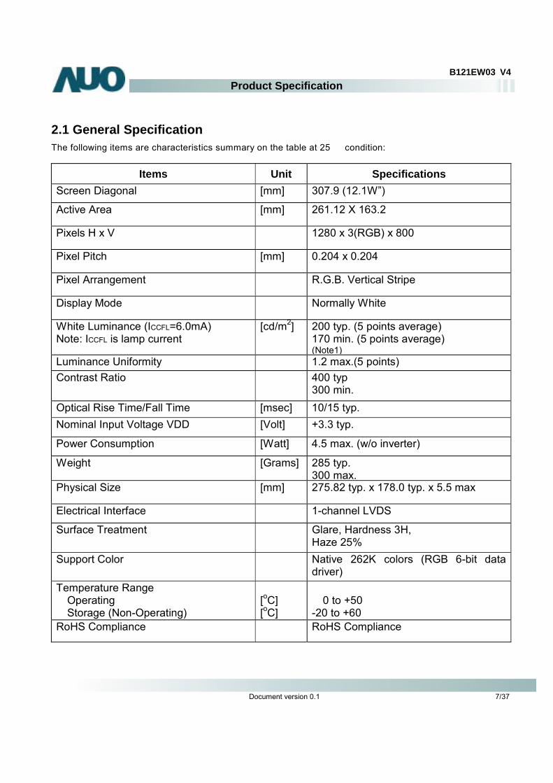
2.1 General Specification
The following items are characteristics summary on the table at 25 ℃ condition:
Items Unit Specifications Screen Diagonal [mm] 307.9 (12.1W”)
Active Area [mm] 261.12 X 163.2
Pixels H x V 1280 x 3(RGB) x 800
Pixel Pitch [mm] 0.204 x 0.204
Pixel Arrangement R.G.B. Vertical Stripe
Display Mode Normally White
White Luminance (ICCFL=6.0mA) Note: ICCFL is lamp current
[cd/m2] 200 typ. (5 points average) 170 min. (5 points average) (Note1)
Luminance Uniformity 1.2 max.(5 points) Contrast Ratio 400 typ
300 min. Optical Rise Time/Fall Time [msec] 10/15 typ. Nominal Input Voltage VDD [Volt] +3.3 typ.
Power Consumption [Watt] 4.5 max. (w/o inverter)
Weight [Grams] 285 typ. 300 max.
Physical Size [mm] 275.82 typ. x 178.0 typ. x 5.5 max
Electrical Interface 1-channel LVDS
Surface Treatment Glare, Hardness 3H, Haze 25%
Support Color Native 262K colors (RGB 6-bit data driver)
Temperature Range Operating Storage (Non-Operating)
[oC] [oC]
0 to +50
-20 to +60 RoHS Compliance RoHS Compliance
Document version 0.1 8/37
Product SpecificationB121EW03 V4
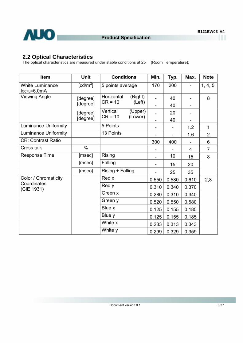
2.2 Optical Characteristics The optical characteristics are measured under stable conditions at 25 (Room Temperature)℃ :
Item Unit Conditions Min. Typ. Max. Note
White Luminance ICCFL=6.0mA
[cd/m2]
5 points average
170 200 - 1, 4, 5.
[degree] [degree]
Horizontal (Right) CR = 10 (Left)
- -
40 40
- -
Viewing Angle
[degree] [degree]
Vertical (Upper)CR = 10 (Lower)
- -
20 40
- -
8
Luminance Uniformity 5 Points - - 1.2 1 Luminance Uniformity 13 Points - - 1.6 2 CR: Contrast Ratio 300 400 - 6 Cross talk % - - 4 7
[msec] Rising - 10 15 [msec] Falling - 15 20
Response Time
[msec] Rising + Falling - 25 35
8
Red x 0.550 0.580 0.610 Red y 0.310 0.340 0.370 Green x 0.280 0.310 0.340 Green y 0.520 0.550 0.580 Blue x 0.125 0.155 0.185 Blue y 0.125 0.155 0.185 White x 0.283 0.313 0.343
Color / Chromaticity Coordinates (CIE 1931)
White y 0.299 0.329 0.359
2,8
Document version 0.1 9/37
Product SpecificationB121EW03 V4
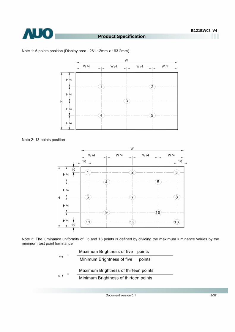
Note 1: 5 points position (Display area : 261.12mm x 163.2mm)
1 2
3
4 5
H /4
H /4
H /4
H /4
H
W
W /4 W /4 W /4 W /4
Note 2: 13 points position
W /4
W
W /4
H
H /4
H /4
H /4
H /4
7
9 1 0
W /4
1
8
W /4
1 0
1 0
1 0
1 0
2 3
1 31 2
4 5
6
1 1
Note 3: The luminance uniformity of 5 and 13 points is defined by dividing the maximum luminance values by the minimum test point luminance
δW13 =
Maximum Brightness of thirteen points
Minimum Brightness of thirteen points
Maximum Brightness of five points δW5 =
Minimum Brightness of five points
Document version 0.1 10/37
Product SpecificationB121EW03 V4
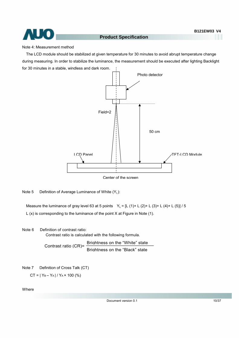
Note 4: Measurement method
The LCD module should be stabilized at given temperature for 30 minutes to avoid abrupt temperature change
during measuring. In order to stabilize the luminance, the measurement should be executed after lighting Backlight
for 30 minutes in a stable, windless and dark room.
Note 5: Definition of Average Luminance of White (YL):
Measure the luminance of gray level 63 at 5 points,YL = [L (1)+ L (2)+ L (3)+ L (4)+ L (5)] / 5
L (x) is corresponding to the luminance of the point X at Figure in Note (1).
Note 6: Definition of contrast ratio:
Contrast ratio is calculated with the following formula.
Note 7: Definition of Cross Talk (CT)
CT = | YB – YA | / YA × 100 (%)
Where
Center of the screen
TFT-LCD Module
50 cm
Photo detector
LCD Panel
Field=2°
Contrast ratio (CR)= Brightness on the “White” stateBrightness on the “Black” state
Document version 0.1 11/37
Product SpecificationB121EW03 V4
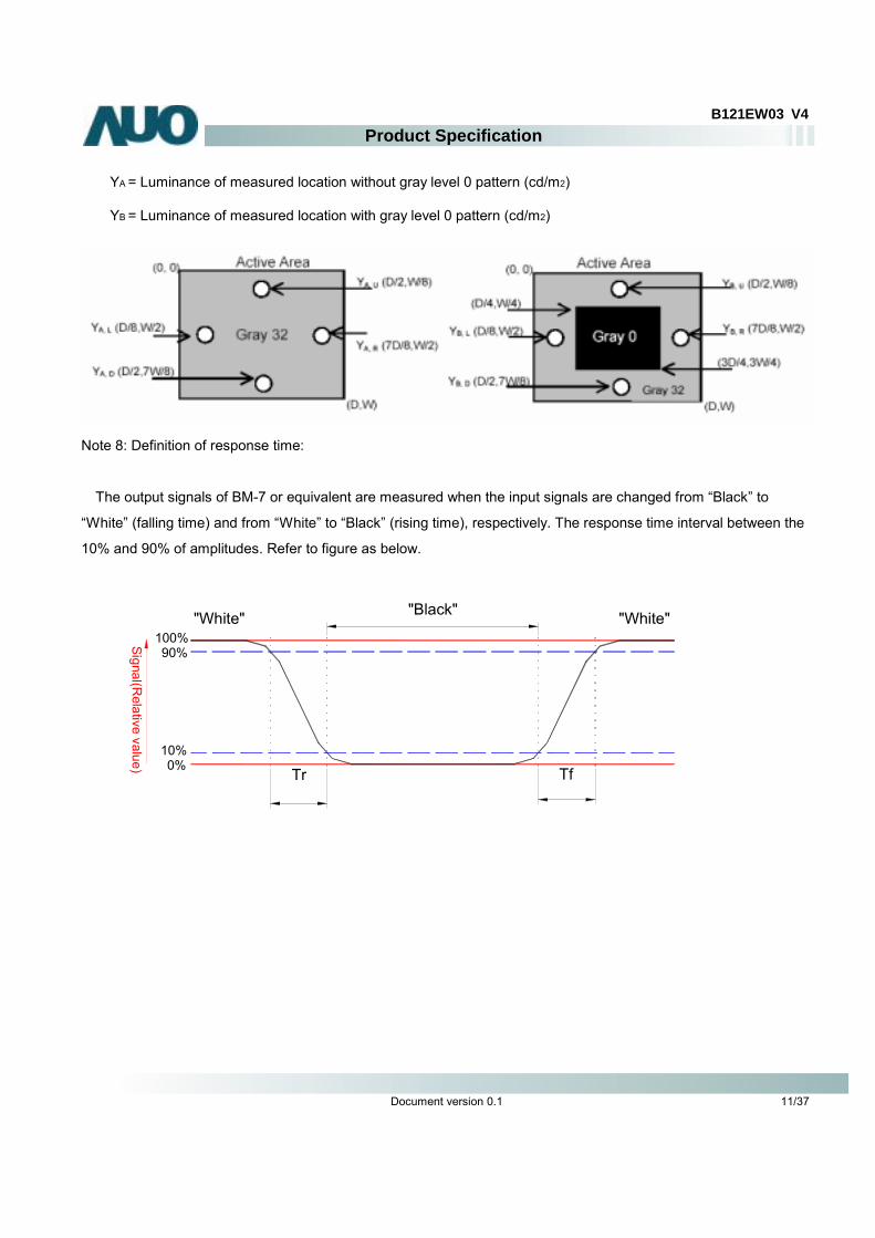
YA = Luminance of measured location without gray level 0 pattern (cd/m2)
YB = Luminance of measured location with gray level 0 pattern (cd/m2)
Note 8: Definition of response time:
The output signals of BM-7 or equivalent are measured when the input signals are changed from “Black” to
“White” (falling time) and from “White” to “Black” (rising time), respectively. The response time interval between the
10% and 90% of amplitudes. Refer to figure as below.
Signal (Relative value)
"Black"
Tr Tf
"White""White"
0%10%
90%100%
Document version 0.1 12/37
Product SpecificationB121EW03 V4
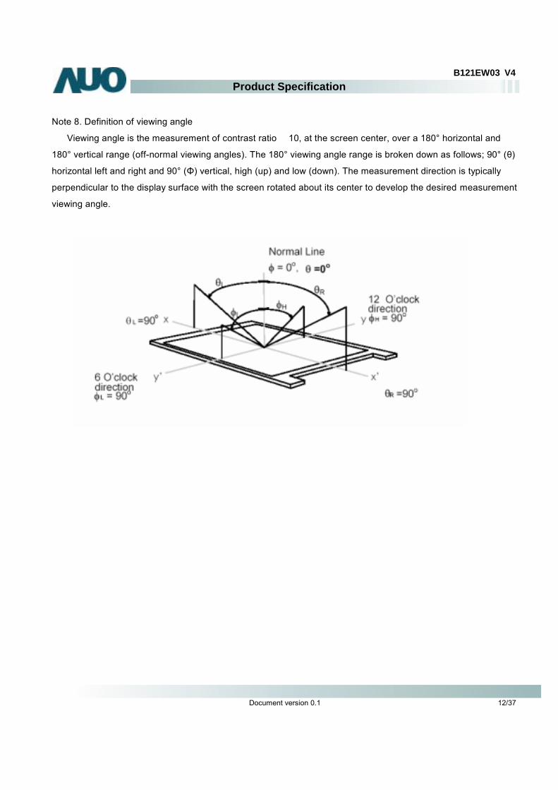
Note 8. Definition of viewing angle
Viewing angle is the measurement of contrast ratio 10, at the screen center, over a 180° horizontal and ≧
180° vertical range (off-normal viewing angles). The 180° viewing angle range is broken down as follows; 90° (θ)
horizontal left and right and 90° (Φ) vertical, high (up) and low (down). The measurement direction is typically
perpendicular to the display surface with the screen rotated about its center to develop the desired measurement
viewing angle.
Document version 0.1 13/37
Product SpecificationB121EW03 V4
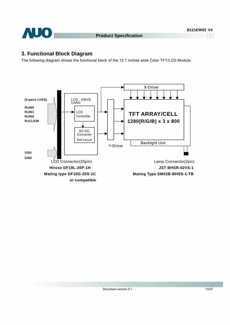
3. Functional Block Diagram The following diagram shows the functional block of the 12.1 inches wide Color TFT/LCD Module:
TFT ARRAY/CELL
VDD
LCD Controller
LCD DRIVE CARD
Backlight Unit
1280(R/G/B) x 3 x 800
GND
DC-DC Converter Ref circuit
Y-Driver
X-Driver
RxIN0 RxIN1 RxIN2 RxCLKIN
(4 pairs LVDS)
Hirose DF19L-20P-1H Mating type DF19G-20S-1C
or compatible
JST BHSR-02VS-1Mating Type SM02B-BHSS-1-TB
Lamp Connector(2pin)LCD Connector(20pin)
Document version 0.1 14/37
Product SpecificationB121EW03 V4
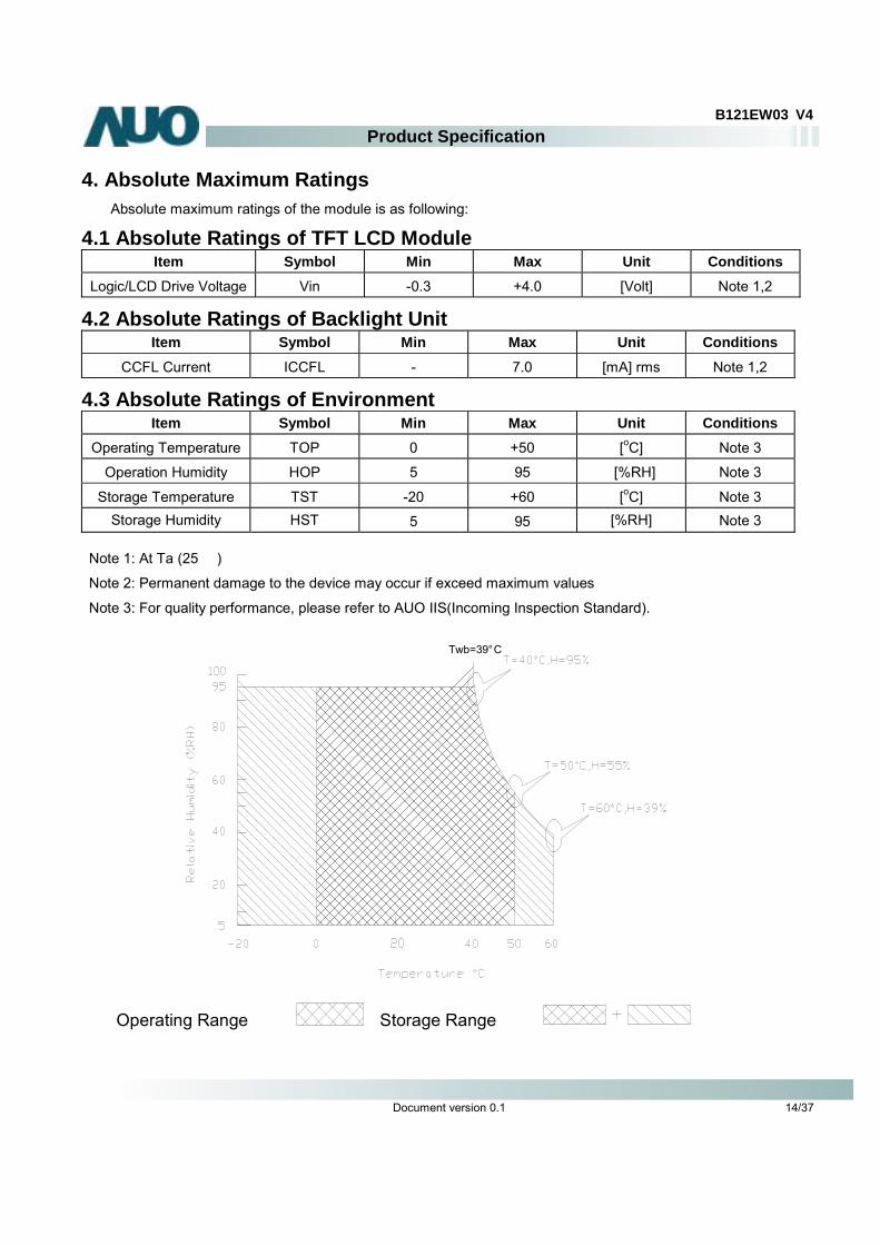
4. Absolute Maximum Ratings Absolute maximum ratings of the module is as following:
4.1 Absolute Ratings of TFT LCD Module Item Symbol Min Max Unit Conditions
Logic/LCD Drive Voltage Vin -0.3 +4.0 [Volt] Note 1,2
4.2 Absolute Ratings of Backlight Unit Item Symbol Min Max Unit Conditions
CCFL Current ICCFL - 7.0 [mA] rms Note 1,2
4.3 Absolute Ratings of Environment Item Symbol Min Max Unit Conditions
Operating Temperature TOP 0 +50 [oC] Note 3
Operation Humidity HOP 5 95 [%RH] Note 3
Storage Temperature TST -20 +60 [oC] Note 3 Storage Humidity HST 5 95 [%RH] Note 3
Note 1: At Ta (25 )℃
Note 2: Permanent damage to the device may occur if exceed maximum values
Note 3: For quality performance, please refer to AUO IIS(Incoming Inspection Standard).
Twb=39°C
Operating Range Storage Range
Document version 0.1 15/37
Product SpecificationB121EW03 V4
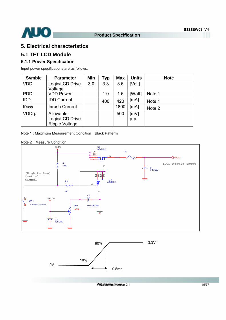
5. Electrical characteristics 5.1 TFT LCD Module 5.1.1 Power Specification Input power specifications are as follows;
Symble Parameter Min Typ Max Units Note VDD Logic/LCD Drive
Voltage 3.0 3.3 3.6 [Volt]
PDD VDD Power 1.0 1.6 [Watt] Note 1 IDD IDD Current 400 420 [mA] Note 1 IRush Inrush Current 1800 [mA] Note 2 VDDrp Allowable
Logic/LCD Drive Ripple Voltage
500 [mV] p-p
Note 1 : Maximum Measurement Condition:Black Patterm
Note 2:Measure Condition +5.0V
+12.0V
VCC
R147K
R2
1K
VR1
47K
SW1
SW MAG-SPST
12
F1
Q3AO6402
G
D2
SD
1
D5
D6
C11uF/16V
Q3AO6402
G
D2 SD1
D5D6
C3
0.01uF/25V
C21uF/25V
(High to Low)ControlSignal
(LCD Module Input)
90%
10%
Vin rising time
0V
3.3V
0.5ms
Document version 0.1 16/37
Product SpecificationB121EW03 V4
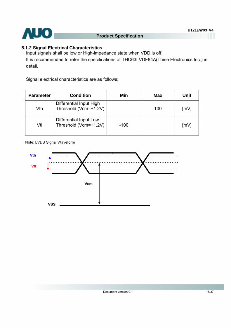
5.1.2 Signal Electrical Characteristics Input signals shall be low or High-impedance state when VDD is off. It is recommended to refer the specifications of THC63LVDF84A(Thine Electronics Inc.) in detail. Signal electrical characteristics are as follows;
Parameter Condition Min Max Unit
Vth
Differential Input High Threshold (Vcm=+1.2V)
100
[mV]
Vtl
Differential Input Low Threshold (Vcm=+1.2V)
-100
[mV]
Note: LVDS Signal Waveform
Vth
Vtl
Vcm
VSS
Document version 0.1 17/37
Product SpecificationB121EW03 V4
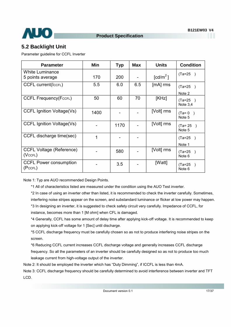
5.2 Backlight Unit Parameter guideline for CCFL Inverter
Parameter Min Typ Max Units Condition White Luminance 5 points average
170
200
-
[cd/m2 ]
(Ta=25 )℃
CCFL current(ICCFL) 5.5 6.0 6.5 [mA] rms (Ta=25 )℃
Note 2 CCFL Frequency(FCCFL) 50 60 70 [KHz] (Ta=25 )℃
Note 3,4
CCFL Ignition Voltage(Vs) 1400 - - [Volt] rms (Ta= 0 )℃ Note 5
CCFL Ignition Voltage(Vs) - 1170 - [Volt] rms (Ta= 25 )℃ Note 5
CCFL discharge time(sec) 1 - - (Ta=25℃)
Note 1 CCFL Voltage (Reference) (VCCFL)
- 580 - [Volt] rms (Ta=25 )℃ Note 6
CCFL Power consumption (PCCFL)
- 3.5 - [Watt] (Ta=25 )℃ Note 6
Note 1: Typ are AUO recommended Design Points.
*1 All of characteristics listed are measured under the condition using the AUO Test inverter.
*2 In case of using an inverter other than listed, it is recommended to check the inverter carefully. Sometimes,
interfering noise stripes appear on the screen, and substandard luminance or flicker at low power may happen.
*3 In designing an inverter, it is suggested to check safety circuit very carefully. Impedance of CCFL, for
instance, becomes more than 1 [M ohm] when CFL is damaged.
*4 Generally, CCFL has some amount of delay time after applying kick-off voltage. It is recommended to keep
on applying kick-off voltage for 1 [Sec] until discharge.
*5 CCFL discharge frequency must be carefully chosen so as not to produce interfering noise stripes on the
screen.
*6 Reducing CCFL current increases CCFL discharge voltage and generally increases CCFL discharge
frequency. So all the parameters of an inverter should be carefully designed so as not to produce too much
leakage current from high-voltage output of the inverter.
Note 2: It should be employed the inverter which has “Duty Dimming”, if ICCFL is less than 4mA.
Note 3: CCFL discharge frequency should be carefully determined to avoid interference between inverter and TFT
LCD.
Document version 0.1 18/37
Product SpecificationB121EW03 V4
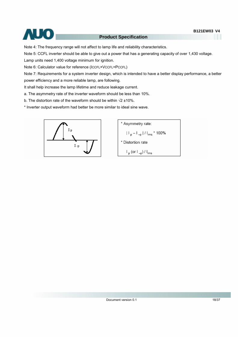
Note 4: The frequency range will not affect to lamp life and reliability characteristics.
Note 5: CCFL inverter should be able to give out a power that has a generating capacity of over 1,430 voltage.
Lamp units need 1,400 voltage minimum for ignition.
Note 6: Calculator value for reference (ICCFL×VCCFL=PCCFL)
Note 7: Requirements for a system inverter design, which is intended to have a better display performance, a better
power efficiency and a more reliable lamp, are following.
It shall help increase the lamp lifetime and reduce leakage current.
a. The asymmetry rate of the inverter waveform should be less than 10%.
b. The distortion rate of the waveform should be within √2 ±10%.
* Inverter output waveform had better be more similar to ideal sine wave.
Document version 0.1 19/37
Product SpecificationB121EW03 V4
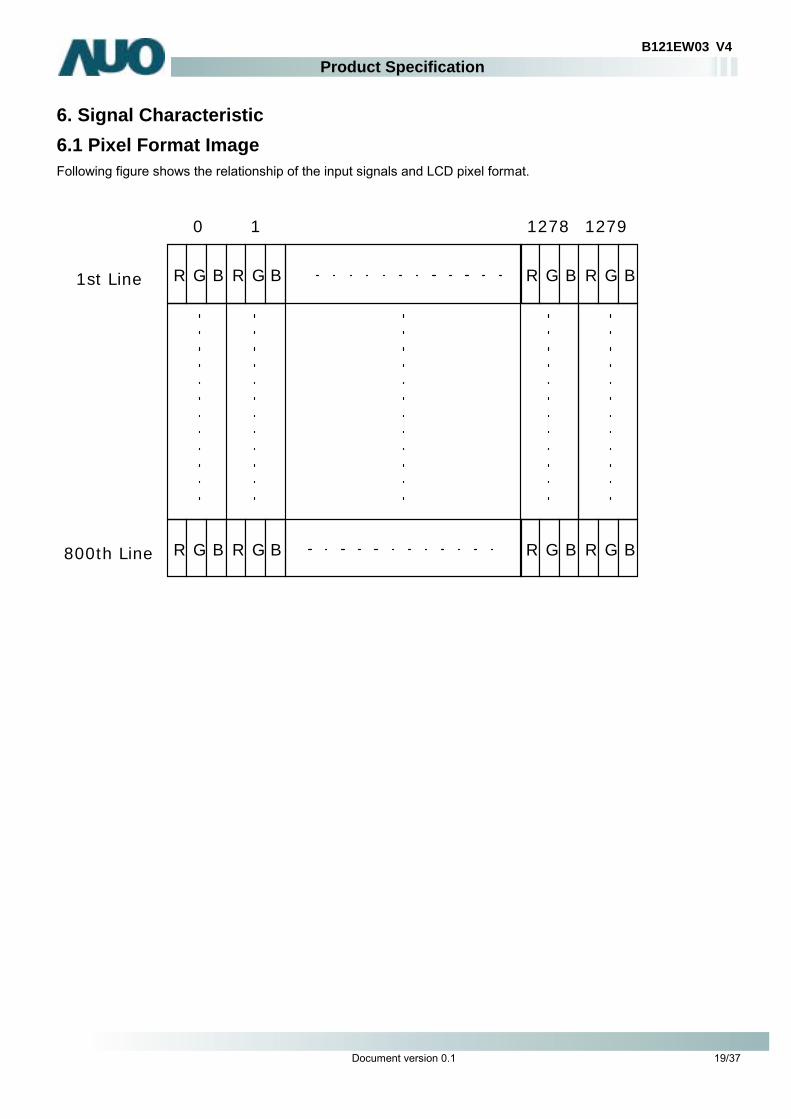
6. Signal Characteristic 6.1 Pixel Format Image Following figure shows the relationship of the input signals and LCD pixel format.
R G B R G B
R G B R G B
R G B R G B
R G B R G B
0 1 1278 1279
1st Line
800th Line
Document version 0.1 20/37
Product SpecificationB121EW03 V4
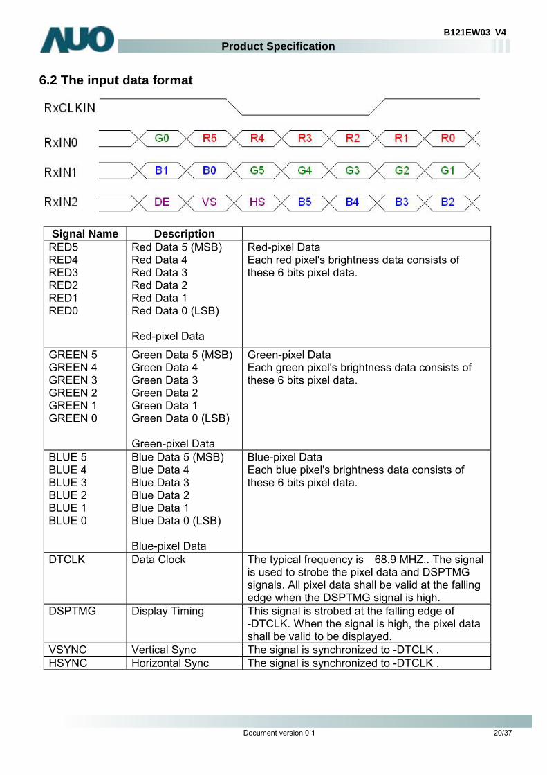
6.2 The input data format
Signal Name Description
RED5 RED4 RED3 RED2 RED1 RED0
Red Data 5 (MSB) Red Data 4 Red Data 3 Red Data 2 Red Data 1 Red Data 0 (LSB) Red-pixel Data
Red-pixel Data Each red pixel's brightness data consists of these 6 bits pixel data.
GREEN 5 GREEN 4 GREEN 3 GREEN 2 GREEN 1 GREEN 0
Green Data 5 (MSB) Green Data 4 Green Data 3 Green Data 2 Green Data 1 Green Data 0 (LSB) Green-pixel Data
Green-pixel Data Each green pixel's brightness data consists of these 6 bits pixel data.
BLUE 5 BLUE 4 BLUE 3 BLUE 2 BLUE 1 BLUE 0
Blue Data 5 (MSB) Blue Data 4 Blue Data 3 Blue Data 2 Blue Data 1 Blue Data 0 (LSB) Blue-pixel Data
Blue-pixel Data Each blue pixel's brightness data consists of these 6 bits pixel data.
DTCLK Data Clock The typical frequency is 68.9 MHZ.. The signal is used to strobe the pixel data and DSPTMG signals. All pixel data shall be valid at the falling edge when the DSPTMG signal is high.
DSPTMG Display Timing This signal is strobed at the falling edge of -DTCLK. When the signal is high, the pixel data shall be valid to be displayed.
VSYNC Vertical Sync The signal is synchronized to -DTCLK . HSYNC Horizontal Sync The signal is synchronized to -DTCLK .
Document version 0.1 21/37
Product SpecificationB121EW03 V4
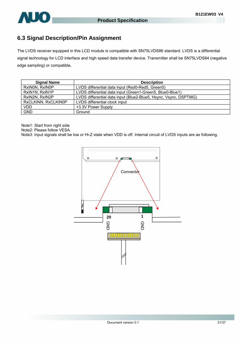
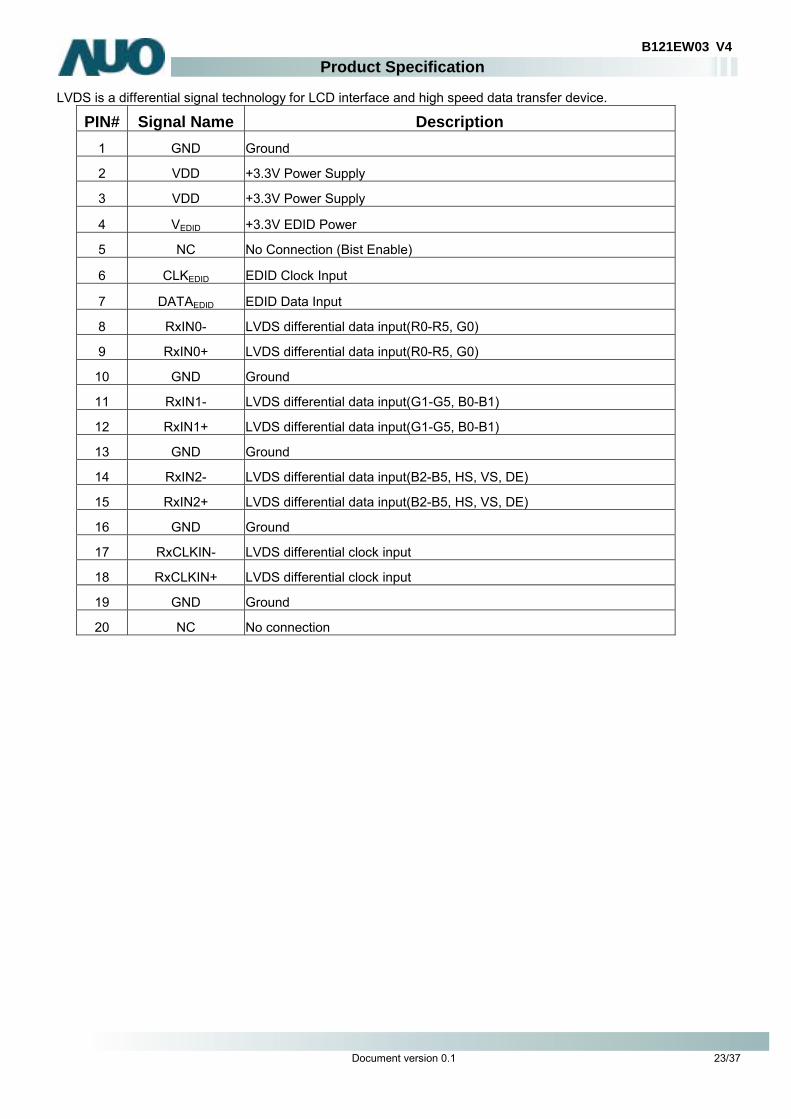
6.3 Signal Description/Pin Assignment
The LVDS receiver equipped in this LCD module is compatible with SN75LVDS86 standard. LVDS is a differential
signal technology for LCD interface and high speed data transfer device. Transmitter shall be SN75LVDS84 (negative
edge sampling) or compatible.
Signal Name Description RxIN0N, RxIN0P LVDS differential data input (Red0-Red5, Green0) RxIN1N, RxIN1P LVDS differential data input (Green1-Green5, Blue0-Blue1) RxIN2N, RxIN2P LVDS differential data input (Blue2-Blue5, Hsync, Vsync, DSPTMG) RxCLKINN, RxCLKIN0P LVDS differential clock input VDD +3.3V Power Supply GND Ground
Note1: Start from right side
Note2: Please follow VESA. Note3: Input signals shall be low or Hi-Z state when VDD is off. Internal circuit of LVDS inputs are as following.
Connector
20 1
GN
D
GN
D
Document version 0.1 22/37
Product SpecificationB121EW03 V4
The module uses a 100ohm resistor between positive and negative data lines of each receiver input
R
R
R
R
Signal Input
Pin No.
9
11
12
14
15
17
18
8
RxIN0+
RxIN0-
RxIN1+
RxIN1-
RxIN2+
RxIN2-
RxCLKIN+
RxCLKIN-
LVDS Receiver
Document version 0.1 23/37
Product SpecificationB121EW03 V4
LVDS is a differential signal technology for LCD interface and high speed data transfer device.
PIN# Signal Name Description 1 GND Ground 2 VDD +3.3V Power Supply 3 VDD +3.3V Power Supply 4 VEDID +3.3V EDID Power 5 NC No Connection (Bist Enable) 6 CLKEDID EDID Clock Input 7 DATAEDID EDID Data Input 8 RxIN0- LVDS differential data input(R0-R5, G0) 9 RxIN0+ LVDS differential data input(R0-R5, G0) 10 GND Ground 11 RxIN1- LVDS differential data input(G1-G5, B0-B1) 12 RxIN1+ LVDS differential data input(G1-G5, B0-B1) 13 GND Ground 14 RxIN2- LVDS differential data input(B2-B5, HS, VS, DE) 15 RxIN2+ LVDS differential data input(B2-B5, HS, VS, DE) 16 GND Ground 17 RxCLKIN- LVDS differential clock input 18 RxCLKIN+ LVDS differential clock input 19 GND Ground 20 NC No connection
Document version 0.1 24/37
Product SpecificationB121EW03 V4
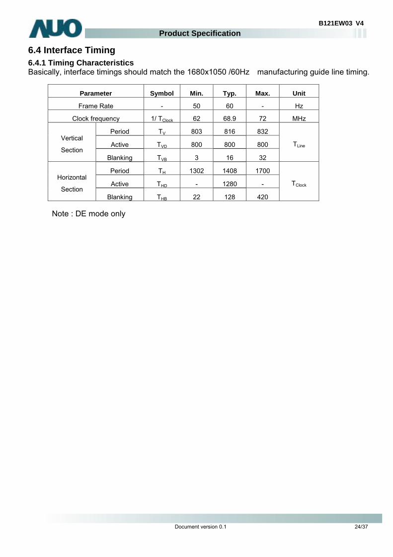
6.4 Interface Timing 6.4.1 Timing Characteristics Basically, interface timings should match the 1680x1050 /60Hz manufacturing guide line timing.
Parameter Symbol Min. Typ. Max. Unit
Frame Rate - 50 60 - Hz
Clock frequency 1/ TClock 62 68.9 72 MHz
Period TV 803 816 832
Active TVD 800 800 800 Vertical
Section Blanking TVB 3 16 32
TLine
Period TH 1302 1408 1700
Active THD - 1280 - Horizontal
Section Blanking THB 22 128 420
TClock
Note : DE mode only
Document version 0.1 25/37
Product SpecificationB121EW03 V4
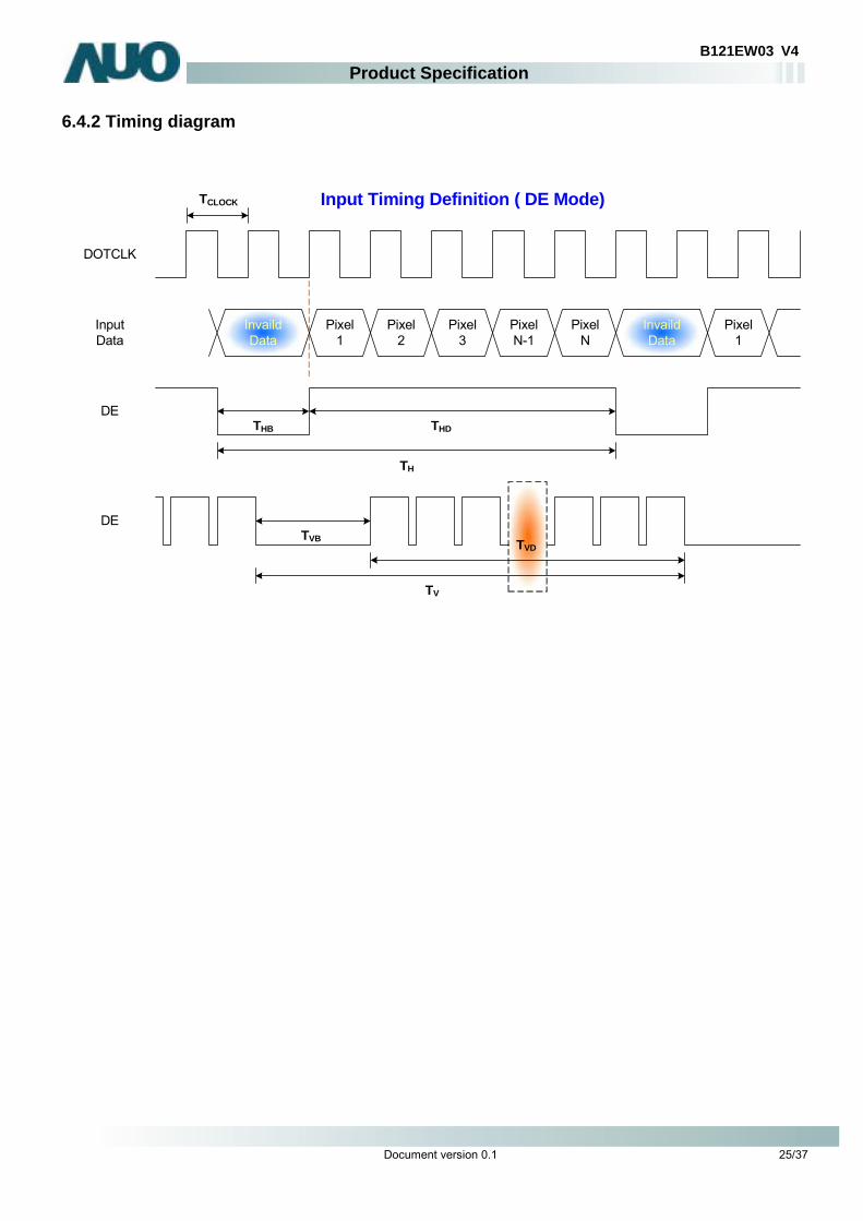
6.4.2 Timing diagram
DOTCLK
DE
TH
THB THD
DE
TV
TVB TVD
Input Timing Definition ( DE Mode) TCLOCK
InputData
Pixel1
Pixel2
Pixel3
PixelN-1
PixelN
InvaildData
InvaildData
Pixel1
Document version 0.1 26/37
Product SpecificationB121EW03 V4
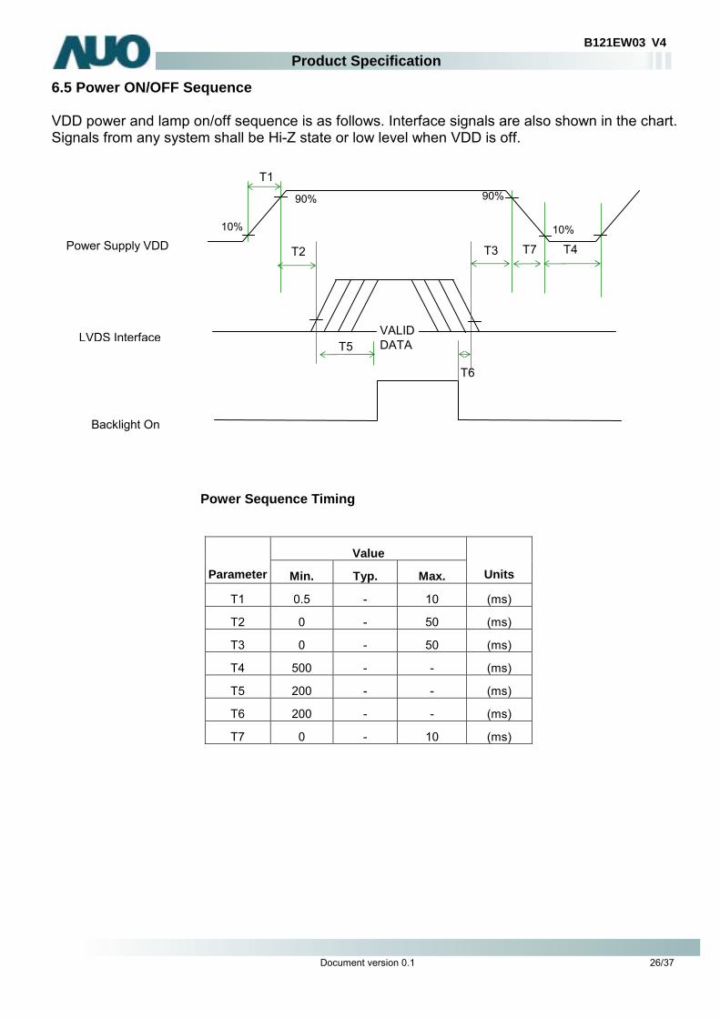
6.5 Power ON/OFF Sequence VDD power and lamp on/off sequence is as follows. Interface signals are also shown in the chart. Signals from any system shall be Hi-Z state or low level when VDD is off.
Power Sequence Timing
Value Parameter Min. Typ. Max. Units
T1 0.5 - 10 (ms) T2 0 - 50 (ms) T3 0 - 50 (ms) T4 500 - - (ms) T5 200 - - (ms) T6 200 - - (ms) T7 0 - 10 (ms)
T4 T3T2
T5 VALID DATA
T1
10%
90%
10%
90%
T6
T7 Power Supply VDD
LVDS Interface
Backlight On
Document version 0.1 27/37
Product SpecificationB121EW03 V4
7. Connector Description
Physical interface is described as for the connector on module.
These connectors are capable of accommodating the following signals and will be following components.
7.1 TFT LCD Module
Connector Name / Designation For Signal Connector
Manufacturer Hirose
Type / Part Number DF19L-20P-1H
Mating Housing/Part Number DF19G-20S-1C or compatible
7.2 Backlight Unit Physical interface is described as for the connector on module.
These connectors are capable of accommodating the following signals and will be following components.
Connector Name / Designation For Lamp Connector
Manufacturer JST
Type / Part Number BHSR-02VS-1
Mating Type / Part Number SM02B-BHSS-1-TB
7.3 Signal for Lamp connector
Pin # Cable color Signal Name 1
Red
Lamp High Voltage
2
White
Lamp Low Voltage
Document version 0.1 28/37
Product SpecificationB121EW03 V4
8. Vibration and Shock Test 8.1 Vibration Test
Test Spec:
Test method: Non-Operation
Acceleration: 1.5G
Frequency: 26 – 500Hz Random
Sweep: 30 Minutes each Axis (X,Y,Z)
8.2 Shock Test Spec: Test Spec:
Test method: Non-Operation
Acceleration: 180 G . Half sine wave
Active time: 2 ms
Pulse: X,Y,Z .one time for each side

Document version 0.1 29/37
Product SpecificationB121EW03 V4
9. Reliability
Items Required Condition Note Temperature Humidity Bias 40 /90%,300Hr℃
High Temperature Operation 50 /Dry,300Hr℃
Low Temperature Operation 0 ,300Hr℃
On/Off Test 25 ,150hrs(ON/10℃ sec. OFF/10sec., 10,000 cycles) Hot Storage 60 /35% RH ,250 hours℃ Cold Storage -20 /50% RH ,250 hours℃ Thermal Shock Test -20 /30 min ,60 /30 min 100cycles℃ ℃ Hot Start Test 50 /1 Hr min. power on/off per 5 minutes, 5 times℃ Cold Start Test 0 /1 Hr℃ min. power on/off per 5 minutes, 5 times Shock Test (Non-Operating) 180G, 2ms, Half-sine wave
Vibration Test (Non-Operating)
Random vibration, 1.5 G zero-to-peak, 26 to 500 Hz, 30 mins in each of three mutually perpendicular axes
ESD Contact : ±8KV/ operation Air : ±15KV / operation
Note 1
Room temperature Test 25 , 2000hours, Operating with loop pattern℃
Note1: According to EN61000-4-2 , ESD class B: Some performance degradation allowed. No data lost
. Self-recoverable. No hardware failures.
Note2: CCFL Life time: 10,000 hours minimum under normal module usage.
Note3: MTBF (Excluding the CCFL): 30,000 hours with a confidence level 90%
Document version 0.1 30/37
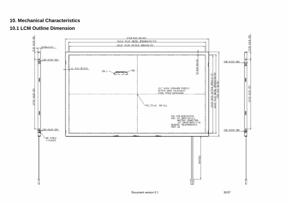
10. Mechanical Characteristics 10.1 LCM Outline Dimension
Document version 0.1 31/37
Document version 0.1 32/37
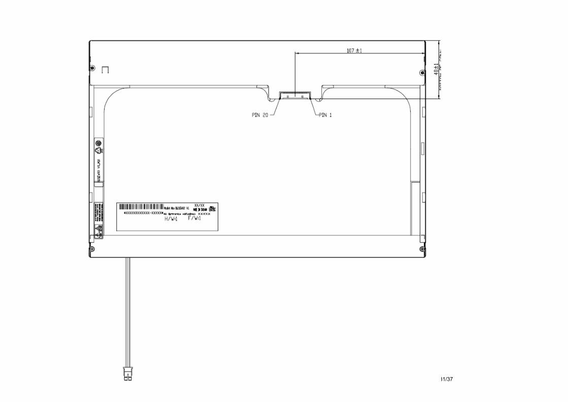
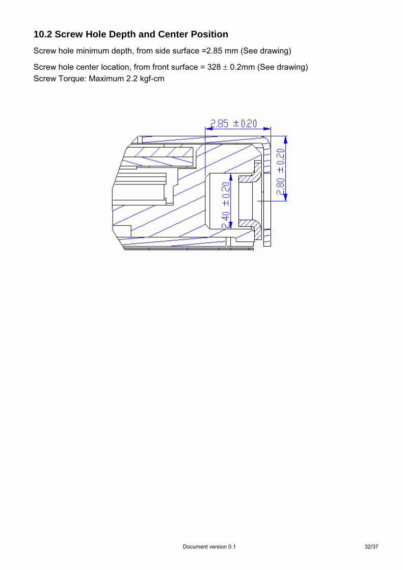
10.2 Screw Hole Depth and Center Position Screw hole minimum depth, from side surface =2.85 mm (See drawing)
Screw hole center location, from front surface = 328 ± 0.2mm (See drawing) Screw Torque: Maximum 2.2 kgf-cm
Document version 0.1 33/37
11. Shipping and Package
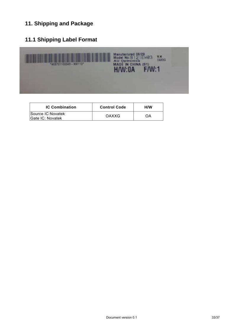
11.1 Shipping Label Format
IC Combination Control Code H/W Source IC:Novatek Gate IC: Novatek OAXXG OA
Document version 0.1 34/37
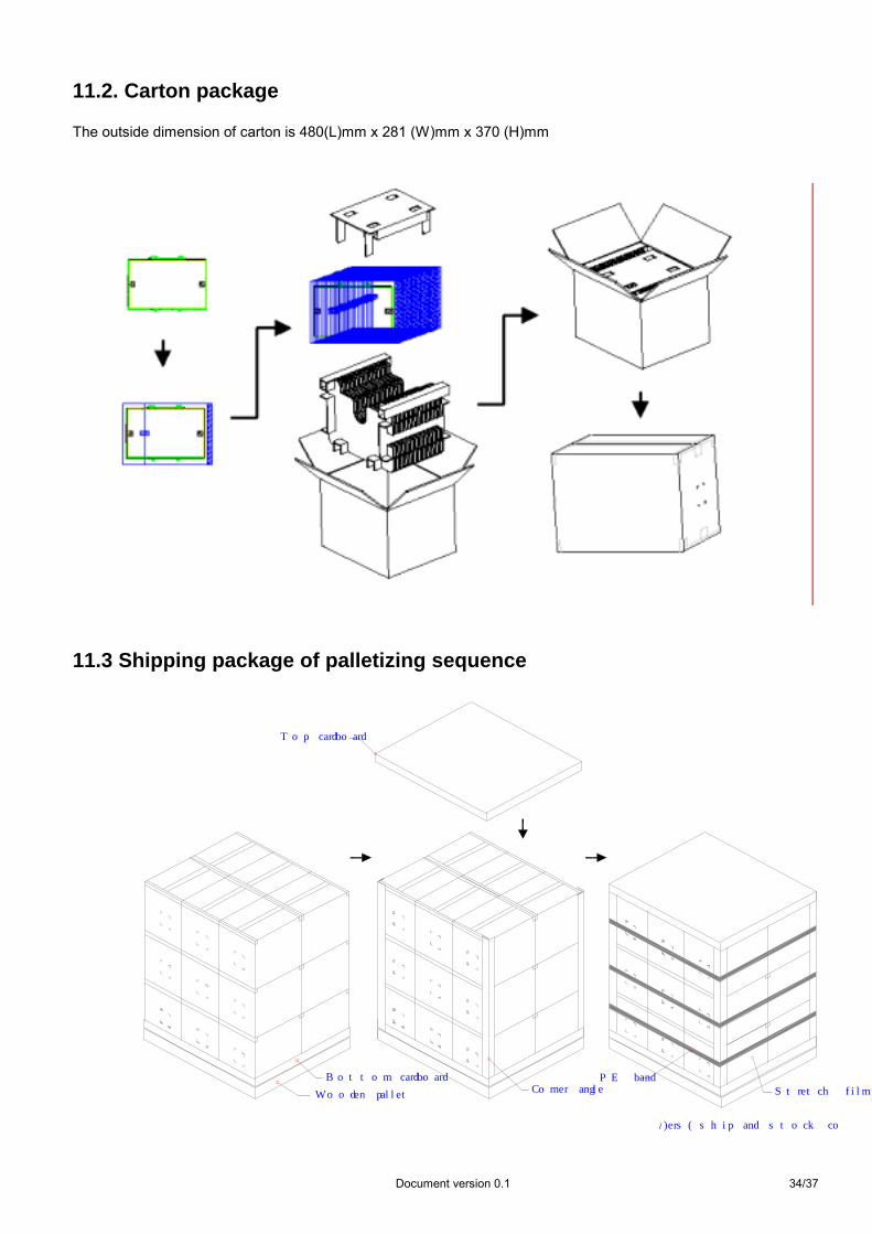
11.2. Carton package The outside dimension of carton is 480(L)mm x 281 (W)mm x 370 (H)mm
11.3 Shipping package of palletizing sequence
Top cardboard
Wooden pallet
Bottom cardboardCorner angle Stretch film
PE band
Note : Limit of box palletizing = Max 3 layers(ship and stock conditions)
Document version 0.1 35/37
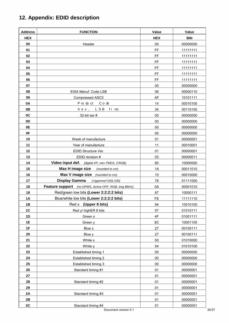
12. Appendix: EDID description
Address FUNCTION Value Value
HEX HEX BIN 00 Header 00 00000000
01 FF 11111111
02 FF 11111111
03 FF 11111111
04 FF 11111111
05 FF 11111111
06 FF 11111111
07 00 00000000
08 EISA Manuf. Code LSB 06 00000110
09 Compressed ASCII AF 10101111
0A Product Code 14 00010100
0B hex, LSB first 34 00110100
0C 32-bit ser # 00 00000000
0D 00 00000000
0E 00 00000000
0F 00 00000000
10 Week of manufacture 01 00000001
11 Year of manufacture 11 00010001
12 EDID Structure Ver. 01 00000001
13 EDID revision # 03 00000011
14 Video input def. (digital I/P, non-TMDS, CRGB) 80 10000000
15 Max H image size (rounded to cm) 1A 00011010
16 Max V image size (rounded to cm) 10 00010000
17 Display Gamma (=(gamma*100)-100) 78 01111000
18 Feature support (no DPMS, Active OFF, RGB, tmg Blk#1) 0A 00001010
19 Red/green low bits (Lower 2:2:2:2 bits) 87 10000111
1A Blue/white low bits (Lower 2:2:2:2 bits) FE 11111110
1B Red x (Upper 8 bits) 94 10010100
1C Red y/ highER 8 bits 57 01010111
1D Green x 4F 01001111
1E Green y 8C 10001100
1F Blue x 27 00100111
20 Blue y 27 00100111
21 White x 50 01010000
22 White y 54 01010100
23 Established timing 1 00 00000000
24 Established timing 2 00 00000000
25 Established timing 3 00 00000000
26 Standard timing #1 01 00000001
27 01 00000001
28 Standard timing #2 01 00000001
29 01 00000001
2A Standard timing #3 01 00000001
2B 01 00000001
2C Standard timing #4 01 00000001
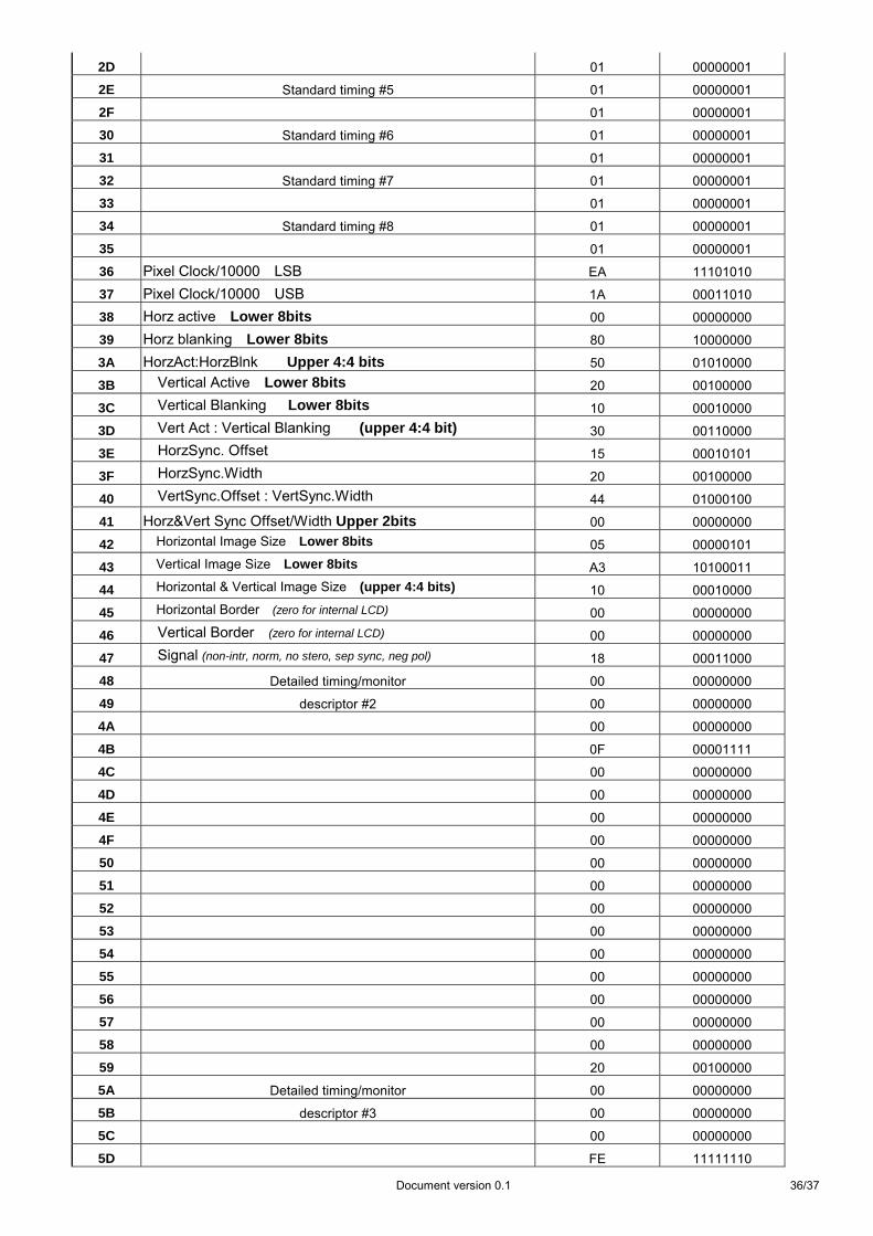
Document version 0.1 36/37
2D 01 00000001
2E Standard timing #5 01 00000001
2F 01 00000001
30 Standard timing #6 01 00000001
31 01 00000001
32 Standard timing #7 01 00000001
33 01 00000001
34 Standard timing #8 01 00000001
35 01 00000001
36 Pixel Clock/10000 LSB EA 11101010
37 Pixel Clock/10000 USB 1A 00011010
38 Horz active Lower 8bits 00 00000000
39 Horz blanking Lower 8bits 80 10000000
3A HorzAct:HorzBlnk Upper 4:4 bits 50 01010000
3B Vertical Active Lower 8bits 20 00100000
3C Vertical Blanking Lower 8bits 10 00010000
3D Vert Act : Vertical Blanking (upper 4:4 bit) 30 00110000
3E HorzSync. Offset 15 00010101
3F HorzSync.Width 20 00100000
40 VertSync.Offset : VertSync.Width 44 01000100
41 Horz&Vert Sync Offset/Width Upper 2bits 00 00000000
42 Horizontal Image Size Lower 8bits 05 00000101
43 Vertical Image Size Lower 8bits A3 10100011
44 Horizontal & Vertical Image Size (upper 4:4 bits) 10 00010000
45 Horizontal Border (zero for internal LCD) 00 00000000
46 Vertical Border (zero for internal LCD) 00 00000000
47 Signal (non-intr, norm, no stero, sep sync, neg pol) 18 00011000
48 Detailed timing/monitor 00 00000000
49 descriptor #2 00 00000000
4A 00 00000000
4B 0F 00001111
4C 00 00000000
4D 00 00000000
4E 00 00000000
4F 00 00000000
50 00 00000000
51 00 00000000
52 00 00000000
53 00 00000000
54 00 00000000
55 00 00000000
56 00 00000000
57 00 00000000
58 00 00000000
59 20 00100000
5A Detailed timing/monitor 00 00000000
5B descriptor #3 00 00000000
5C 00 00000000
5D FE 11111110
Document version 0.1 37/37
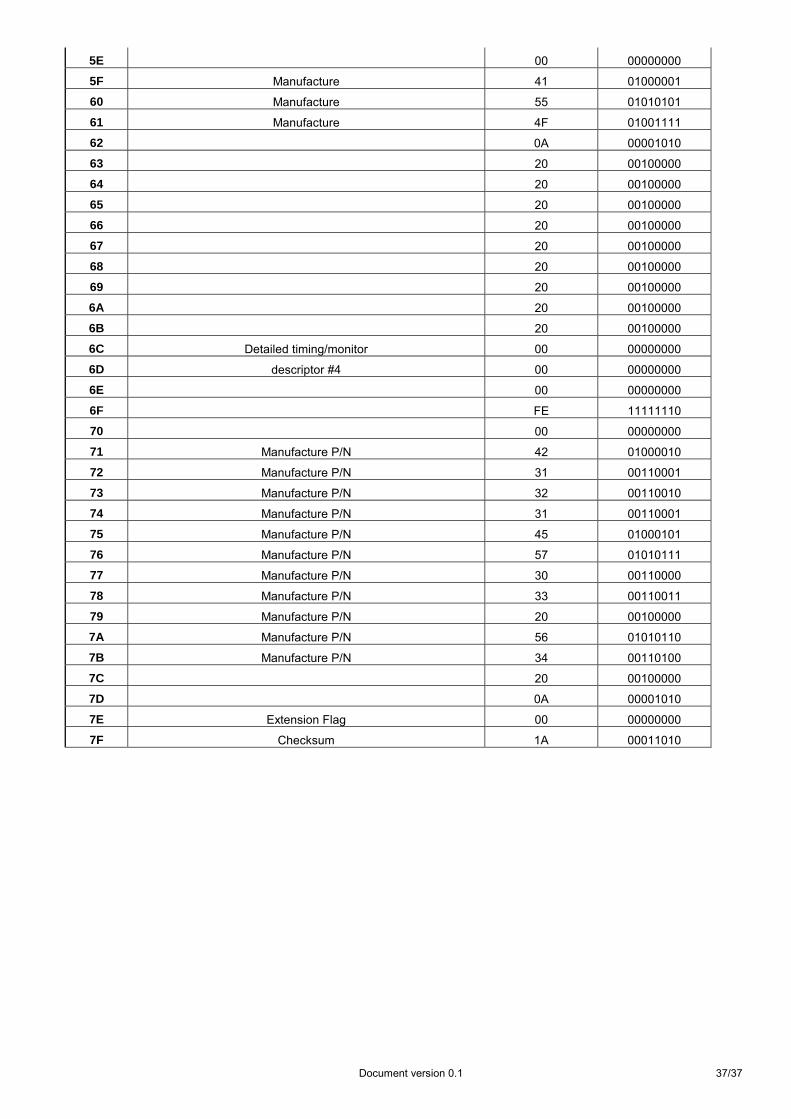
5E 00 00000000
5F Manufacture 41 01000001
60 Manufacture 55 01010101
61 Manufacture 4F 01001111
62 0A 00001010
63 20 00100000
64 20 00100000
65 20 00100000
66 20 00100000
67 20 00100000
68 20 00100000
69 20 00100000
6A 20 00100000
6B 20 00100000
6C Detailed timing/monitor 00 00000000
6D descriptor #4 00 00000000
6E 00 00000000
6F FE 11111110
70 00 00000000
71 Manufacture P/N 42 01000010
72 Manufacture P/N 31 00110001
73 Manufacture P/N 32 00110010
74 Manufacture P/N 31 00110001
75 Manufacture P/N 45 01000101
76 Manufacture P/N 57 01010111
77 Manufacture P/N 30 00110000
78 Manufacture P/N 33 00110011
79 Manufacture P/N 20 00100000
7A Manufacture P/N 56 01010110
7B Manufacture P/N 34 00110100
7C 20 00100000
7D 0A 00001010
7E Extension Flag 00 00000000
7F Checksum 1A 00011010