Embed Size (px)
Citation preview
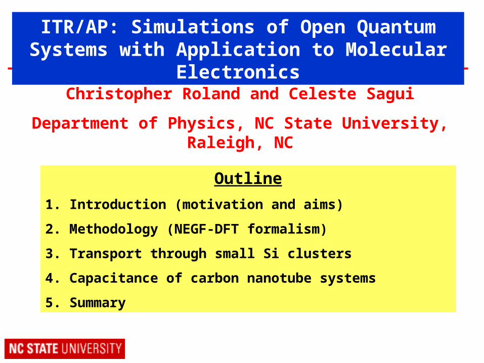
ITR/AP: Simulations of Open Quantum Systems with Application to Molecular Electronics
Christopher Roland and Celeste Sagui
Department of Physics, NC State University, Raleigh, NC
Outline
1. Introduction (motivation and aims)
2. Methodology (NEGF-DFT formalism)
3. Transport through small Si clusters
4. Capacitance of carbon nanotube systems
5. Summary
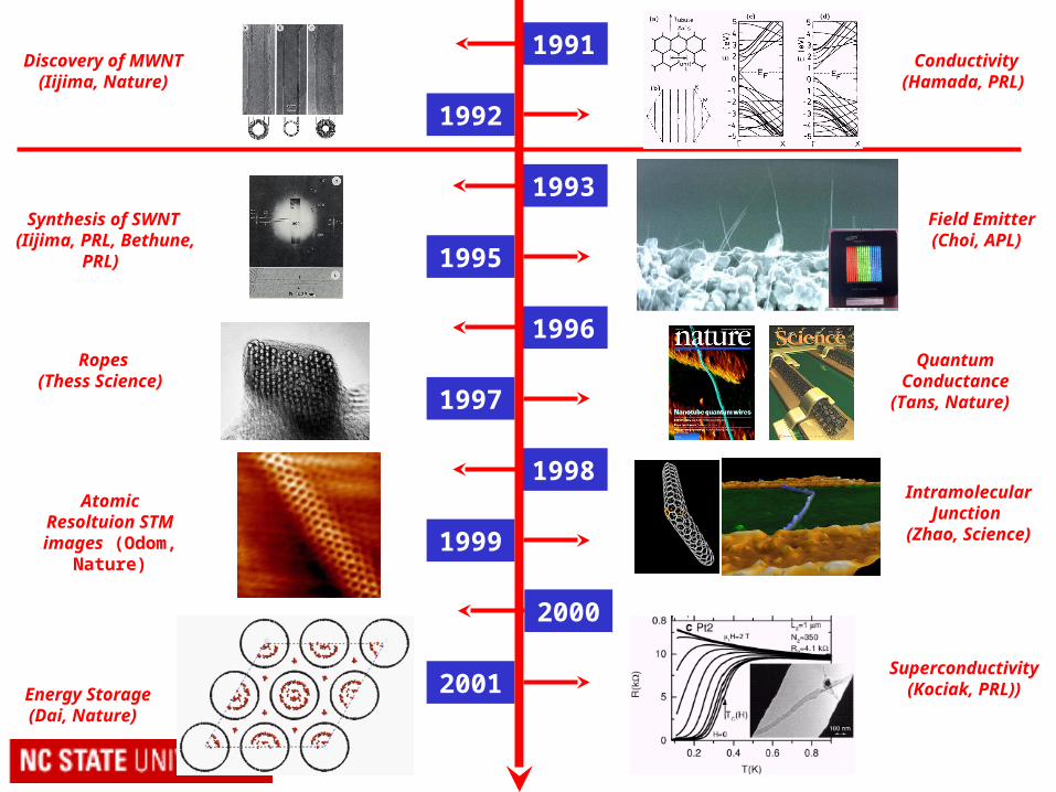
1992
1993
1995
1996
1997
1998
1999
2000
1991Discovery of MWNT
(Iijima, Nature) Conductivity
(Hamada, PRL)
Ropes (Thess Science)
Synthesis of SWNT (Iijima, PRL, Bethune,
PRL)
Field Emitter(Choi, APL)
Superconductivity (Kociak, PRL))
Quantum Conductance
(Tans, Nature)
2001Energy Storage(Dai, Nature)
Atomic Resoltuion STM images (Odom,
Nature)
Intramolecular Junction
(Zhao, Science)
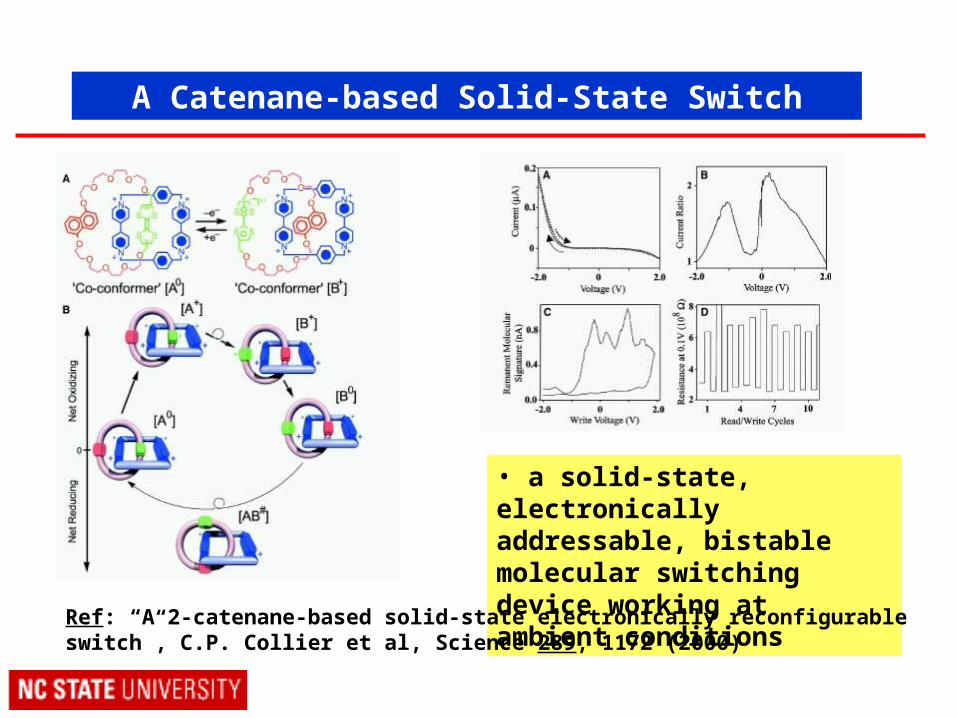
A Catenane-based Solid-State Switch
• a solid-state, electronically addressable, bistable molecular switching device working at ambient conditions
Ref: “A 2-catenane-based solid-state electronically reconfigurable switch”, C.P. Collier et al, Science 289, 1172 (2000)
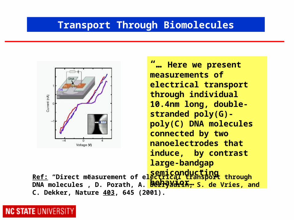
Transport Through Biomolecules
“… Here we present measurements of electrical transport through individual 10.4nm long, double-stranded poly(G)-poly(C) DNA molecules connected by two nanoelectrodes that induce, by contrast large-bandgap semiconducting behavior…”
Ref: “Direct measurement of electrical transport through DNA molecules”, D. Porath, A. Bezryadrin, S. de Vries, and C. Dekker, Nature 403, 645 (2001).
What fundamental aspects of molecular-scale devices need exploration ?
What principles underlie the operation of nanoscale devices?
What controls current flow in molecules ?
What classes of molecules make good devices and sensors?
How to best deal with interactions, far-from equilibrium effects, dynamic response, spin effects, nonlinear coupling of devices, …?Ultimately, one wants to predict the quantum transport characteristics with as few adjustable parameters as possible !
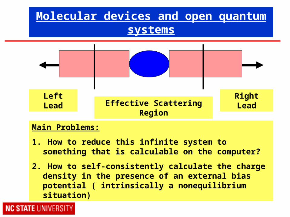
Molecular devices and open quantum systems
Effective Scattering RegionLeft Lead Right Lead
Main Problems:
1. How to reduce this infinite system to something that is calculable on the computer?
2. How to self-consistently calculate the charge density in the presence of an external bias potential ( intrinsically a nonequilibrium situation)
Theoretical Approaches to Quantum Transport
1. Semi-empirical methods: non-selfconsistent methods, typically involving tight-binding Hamiltonians (many authors)
2. Ab initio supercell methods: solve Kohn-Sham equations with periodic boundary conditions; good way to calculate conductances, but not I-V curves (e.g., Choi and Ihm, PRB 59, 2267 (1995) and others)
3. Lippman-Schwinger approach: typically leads are Jellium based with charge density constructed from scattering states (Lang and coworkers)
4. Nonequilibrium Greens function approach: combined with DFT (Taylor, Guo, and Wang, PRB 63, 245407 (2001))**
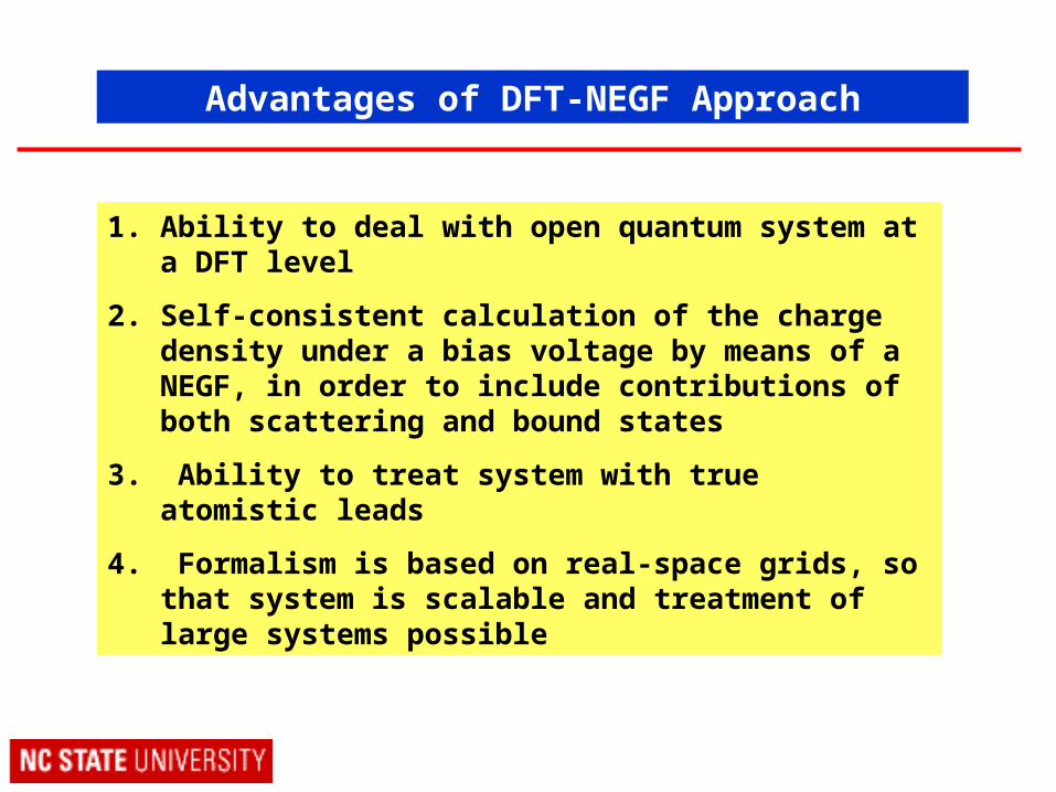
Advantages of DFT-NEGF Approach
1. Ability to deal with open quantum system at a DFT level
2. Self-consistent calculation of the charge density under a bias voltage by means of a NEGF, in order to include contributions of both scattering and bound states
3. Ability to treat system with true atomistic leads
4. Formalism is based on real-space grids, so that system is scalable and treatment of large systems possible
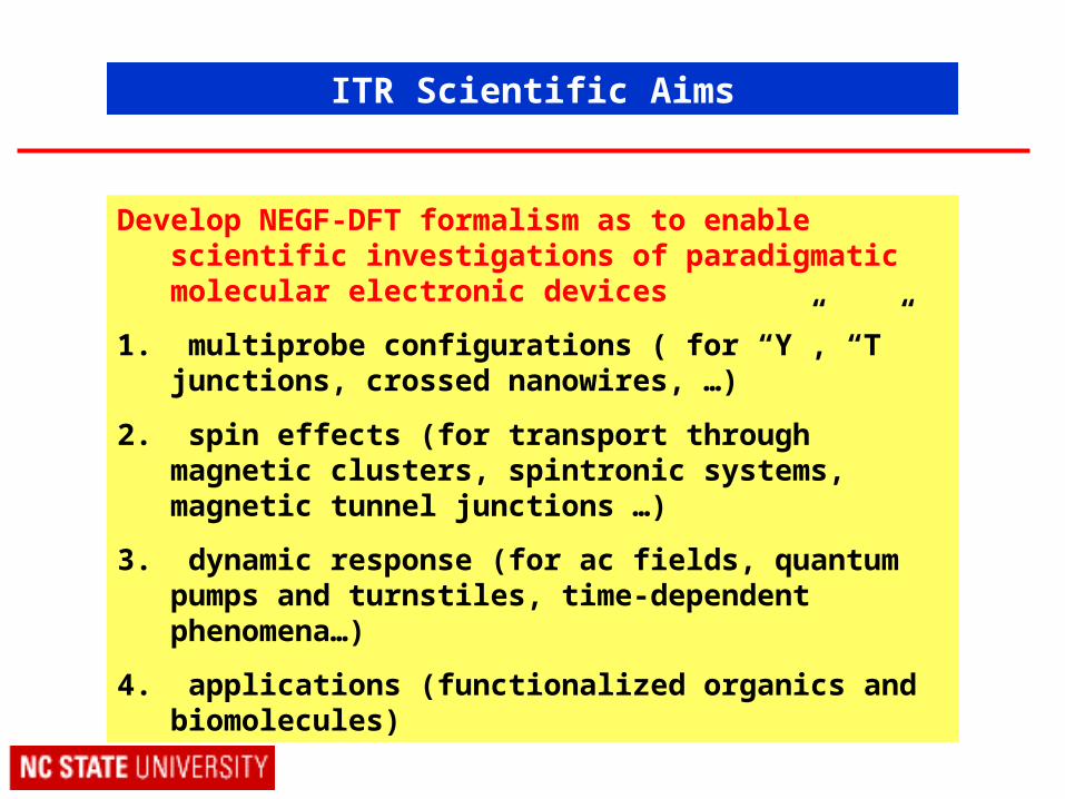
ITR Scientific Aims
Develop NEGF-DFT formalism as to enable scientific investigations of paradigmatic molecular electronic devices
1. multiprobe configurations ( for “Y”, “T” junctions, crossed nanowires, …)
2. spin effects (for transport through magnetic clusters, spintronic systems, magnetic tunnel junctions …)
3. dynamic response (for ac fields, quantum pumps and turnstiles, time-dependent phenomena…)
4. applications (functionalized organics and biomolecules)
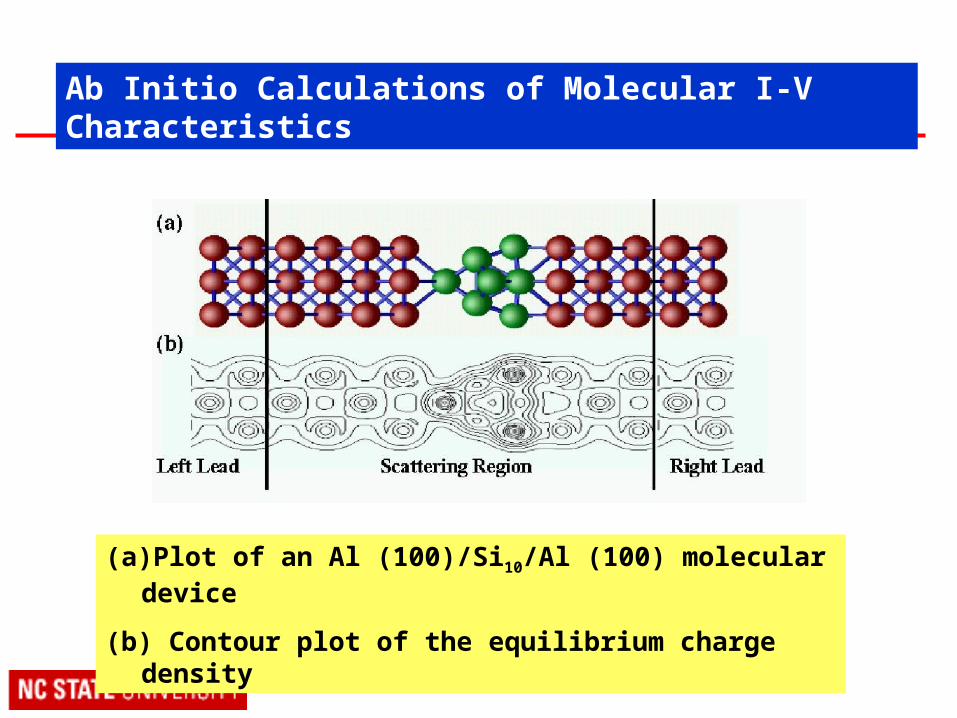
(a)Plot of an Al (100)/Si10/Al (100) molecular device
(b) Contour plot of the equilibrium charge density
Ab Initio Calculations of Molecular I-V Characteristics
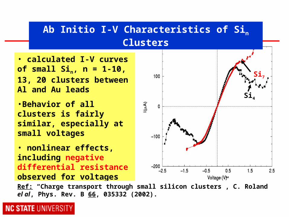
Si4
Si7
• calculated I-V curves of small Sin, n = 1-10, 13, 20 clusters between Al and Au leads
•Behavior of all clusters is fairly similar, especially at small voltages
• nonlinear effects, including negative differential resistance observed for voltages greater than 0.6 V
Ref: “Charge transport through small silicon clusters”, C. Roland el al, Phys. Rev. B 66, 035332 (2002).
Ab Initio I-V Characteristics of Sin Clusters
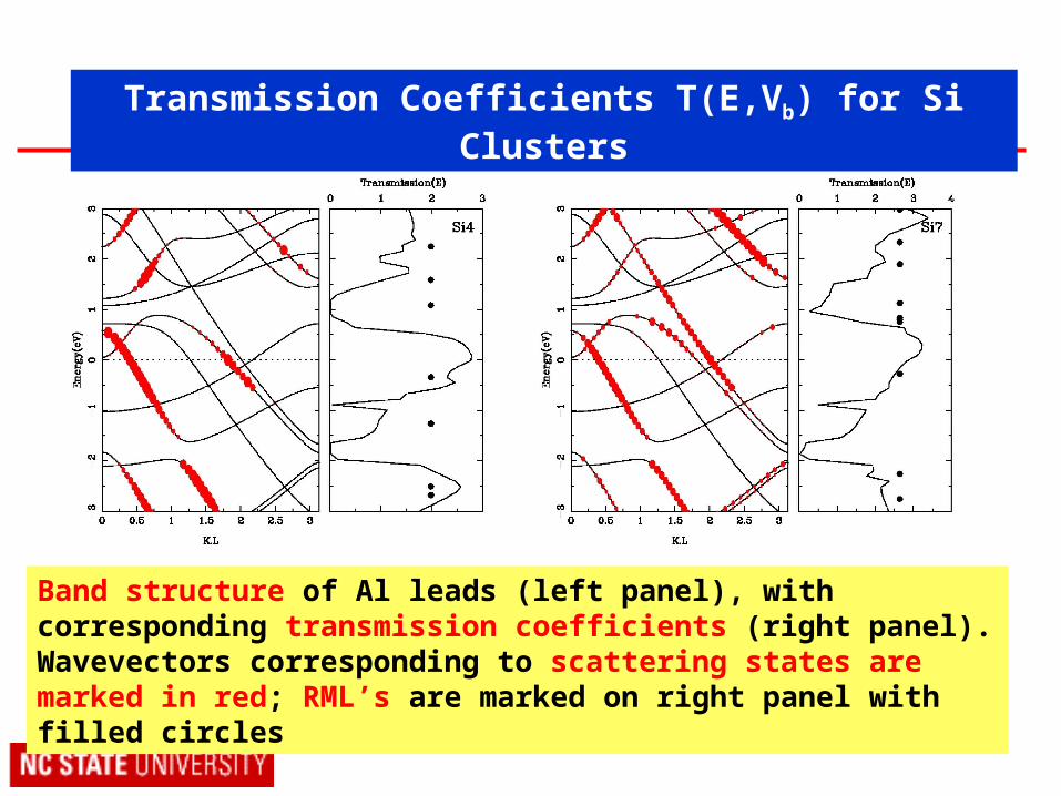
Band structure of Al leads (left panel), with corresponding transmission coefficients (right panel). Wavevectors corresponding to scattering states are marked in red; RML’s are marked on right panel with filled circles
Transmission Coefficients T(E,Vb) for Si Clusters
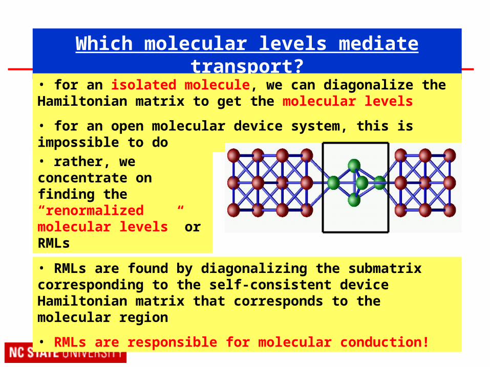
Which molecular levels mediate transport?
• for an isolated molecule, we can diagonalize the Hamiltonian matrix to get the molecular levels
• for an open molecular device system, this is impossible to do
• rather, we concentrate on finding the “renormalized molecular levels” or RMLs
• RMLs are found by diagonalizing the submatrix corresponding to the self-consistent device Hamiltonian matrix that corresponds to the molecular region
• RMLs are responsible for molecular conduction!
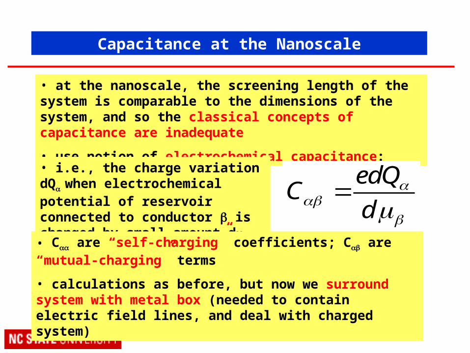
• at the nanoscale, the screening length of the system is comparable to the dimensions of the system, and so the classical concepts of capacitance are inadequate
• use notion of electrochemical capacitance:
edQC
d
• i.e., the charge variation dQ when electrochemical potential of reservoir connected to conductor is changed by small amount d
• C are “self-charging” coefficients; C are “mutual-charging” terms
• calculations as before, but now we surround system with metal box (needed to contain electric field lines, and deal with charged system)
Capacitance at the Nanoscale
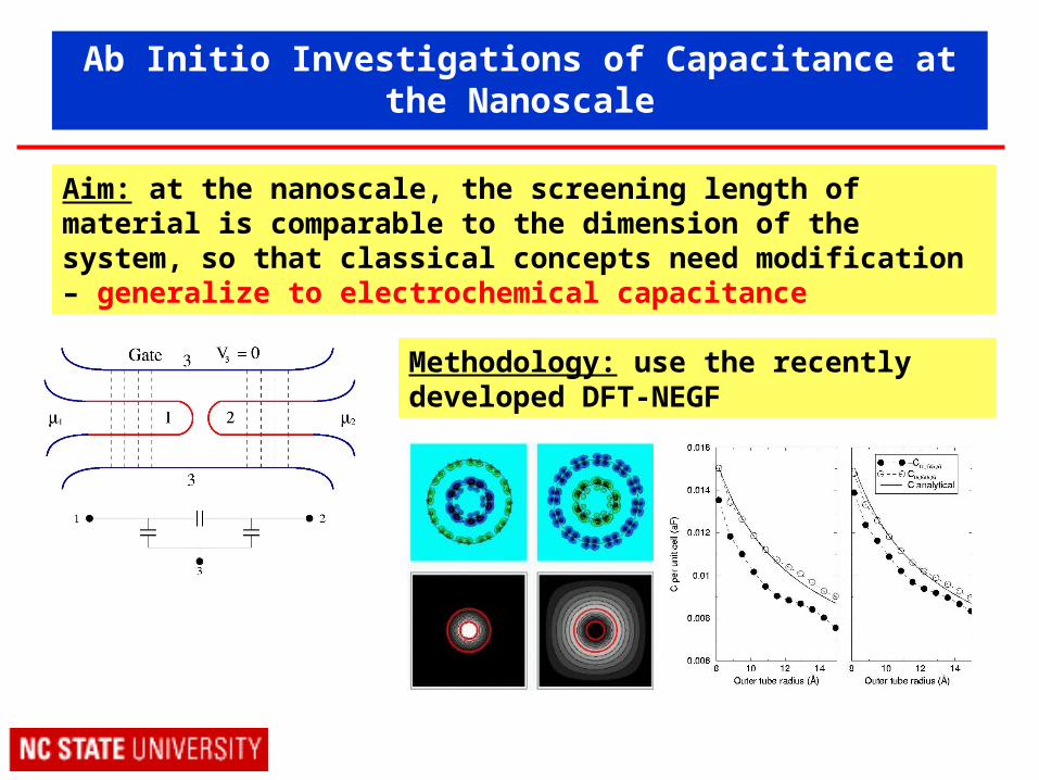
Ab Initio Investigations of Capacitance at the Nanoscale
Aim: at the nanoscale, the screening length of material is comparable to the dimension of the system, so that classical concepts need modification – generalize to electrochemical capacitance
Methodology: use the recently developed DFT-NEGF
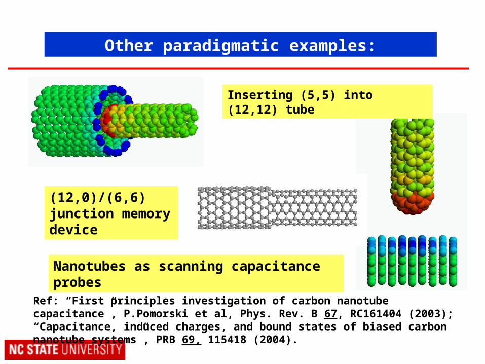
Other paradigmatic examples:
Ref: “First principles investigation of carbon nanotube capacitance”, P.Pomorski et al, Phys. Rev. B 67, RC161404 (2003); “Capacitance, induced charges, and bound states of biased carbon nanotube systems”, PRB 69, 115418 (2004).
Nanotubes as scanning capacitance probes
(12,0)/(6,6) junction memory device
Inserting (5,5) into (12,12) tube
Summary
Aim is to investigate open quantum systems, with application to molecular electronic systems, by means of a recently developed NEGF-DFT formalism
Examples:
I-V characteristics of Si-cluster based devices
Capacitance of carbon nanotubes
![INDIAN INCOME TAX RETURN ACKNOWLEDGEMENT ......[Where the data of the Return of Income in Form ITR-1 (SAHAJ), ITR-2, ITR-3, ITR-4 , ITR-5, ITR-6,ITR-7 filed and verified electronically]](https://img.pdfslide.us/doc/110x75/61250246c71ac647a36c0516/indian-income-tax-return-acknowledgement-where-the-data-of-the-return-of.jpg)


![INDIAN INCOME TAX RETURN ACKNOWLEDGEMENT data the of Income in Form ITR-I (SAHAJ), ITR-2, 'TR-3 i TR. , iTR-5, ITR-6,ITR-7 transmitted electronically with digital signature] PAN](https://img.pdfslide.us/doc/110x75/6124fffffae81757105d8747/-indian-income-tax-return-acknowledgement-data-the-of-income-in-form-itr-i-sahaj.jpg)