Embed Size (px)
Citation preview

1
Welcome to the third newsletter of
CABRISS project!
CABRISS implements a pioneering approach towards a PV circular
economy demonstrating the re-usability and recyclability of key PV
materials for PV and other applications like electronics, metallurgy
and glass industries.
UPCOMING: STANDARDIZATION WORKSHOP
Save the date: TU Vienna is happy to welcome you for the CABRISS
Standardization Seminar. The workshop is free of charge and it will
be held at TU Wien Campus Getreidemarkt 9, 1060 Wien, TutheSky,
11th floor, Wednesday, December 07th, 2016, 12:00 – 16:00
NEWSLETTER Issue: 3
November 2016
www.spire2030.eu/cabriss
CABRISS - Implementation of a
CirculAr economy Based on Recycled,
reused and recovered Indium, Silicon
and Silver materials for photovoltaic
and other applications
H2020-WASTE-2014
Starting date: June 1st, 2015
Project duration: 36 months
Coordinator: CEA-INES
Contact point: David Pelletier
+33(0)-632-218-691
+33(0)-479-792-061
E-mail: [email protected]
This project has received funding from
the European Union's Horizon 2020
research and innovation programme,
under grant agreement No. 641972.

2
Overview
CABRISS Standardisation workshop and activities 2
Report on economic opportunities and markets for PV waste 4
CABRISS – Work in progress 7
STANDARDIZATION WORKSHOP
Save the date: TU Vienna is happy to welcome you for the CABRISS Standardization Seminar.
Venue: TU Wien Campus Getreidemarkt 9, 1060 Wien, TutheSky, 11th floor
Time: Wednesday, December 07th, 2016, 12:00 – 16:00
Integrating research with standardisation has a number of advantages for researchers, businesses,
and for society. Standards can form the foundations for further developments, new research and
ultimately new knowledge, creating a virtuous knowledge circle for standards and research. It is
becoming increasingly important to integrate research results into standards, as well as establish
new areas of standards activities. This leads to better standards and creates the potential for new
business opportunities for European companies. The seminar will be held by Ms. Andreea Gulacsi
Gologan. She will share her valuable experience as a Research Integration Unit Manager at the CEN
and CENELEC - European Standardization Committee. Her key areas of work are coordinating and
facilitating the link between standardization and research, providing support
to the CEN and CENELEC members engaged with Horizon2020 and to
research projects to address standardization in their proposals and projects.
The seminar aims at helping researchers and businesses to understand the
role of standardization in innovation and to address related questions at an
early stage in the development process, thereby supporting market uptake
and exploitation. (CEN – EU Committee for Standardization/ CENELEC - EU
Committee for Electrotechnical Standardization /www.cencenelec.eu).
For information, agenda and registration (participation is free of charge), please contact
Additional information can be found on the project website: www.spire2030.eu/cabriss.

3
STANDARDIZATION
Standardization within CABRISS aims at providing a bridge that connects research to industry. This
is of importance as investors in new technologies have to overcome the critical phase between
demonstration and commercialization. To cross this well-known “valley of death”, a good awareness
and understanding of all pre-requirements for accessing the market is crucial.
Two technology steps are addressed in CABRISS:
- collection of end-of-life modules, cells and PV waste
- dismantling, extraction and recovery
Both are strongly influenced by the European directive WEEE (Waste Electrical and Electronic
Equipment Directive) which became effective on 14th February 2014. WEEE regulates the treatment
of electrical and electronic waste at the end of life cycle.
The Commission requested the European standardization organizations to develop standards for
the recycling treatment, including separation and removal of key components, such as frames, glass,
polymers, plastics and metals, including cables. Among these organisations, CABRISS has established
contacts to SEMI and CEN/CENELEC for a closer interaction and knowledge exchange.
Meanwhile, CABRISS has deepened collaboration with CENELEC’s CLC/TC 111X Environment (prEN
50625-2-4) which deals with collection, logistics and treatment requirements for WEEE- part2-4:
„Specific requirements for the treatment of photovoltaic panels“. In September 2016, the chair of
TC111X invited the CABRISS consortium to comment the draft documents which are expected to be
available in November 2016.
On 10th November 2016, CABRISS was presented to CENELEC’s CLC/TC 111X in Brussels during the
plenary meeting.

4
WASTES FROM SILICON PV MANUFACTURING AND THEIR ECONOMIC VALUE
The CABRISS project aims at providing new technologies and new insights that support a circular
economy for the PV sector. To elucidate the economic environment, the project plan foresees one
deliverable focusing on a thorough market and competitive analysis. The following chapter presents
parts of the analysis.
A number of wastes are generated during the PV cell production process and some of these wastes
can be recycled both in and outside of the PV industry. Today, the two main wastes that are recycled
within the production process are the silicon off-cuts that are created when cutting either the cast
multi-crystalline silicon or the monocrystalline ingot. Much of this high-quality silicon can readily be
recycled within ingot manufacturing and therefore represents closed-loop recycling at this point in
the value chain. The second recycling process that is currently used in the industry involves slurry
recycling.
Whereas ingot block cutting creates silicon waste of generally very high quality that can be easily
recycled within ingot manufacture, the wafering process creates large quantities of silicon kerf
(powder) loss as the result of cutting the ingots into thin (today 180 micron thick) wafers. The
wafering step leads to approximately a 45% loss of silicon volume, and this volume is either in the
form of dry powder, in the case where cutting uses a diamond saw, is the form of silicon powder
mixed with the abrasive (silicon-carbide based) cutting slurry in the case of traditional steel wire
cutting.
Other potential wastes for recycling come from cell and module manufacture, including final
installation. During cell processing, we can define three main stages at which the wafer can
potentially be recycled. If the wafer is broken early on before processing has begun, it can “easily”
be resold to the ingot/wafer maker for re-melting and reintroduction into the process of ingot
manufacture. In the case that cell processing has begun, but before the stage of latter stages of
metallization, the cell can be processed through a series of chemical cleaning and lapping stages
again returned for ingot manufacture (assuming such a process makes economic sense for the cell
maker). In the third situation, in which either a breakage occurs after metallization has begun (or
the final cell is simply not within specification) the cell is much more difficult to recycle, but falls into
the scope of CABRISS, in the sense that the silicon and the silver can in principal be recovered and
used either inside or outside of PV applications. For modules broken during the production process,
the aluminium frame may be easily recoverable for immediate reuse, but panels broken during the
installation process are very similar to end-of-life panels from a recycling perspective.

5
The figure below summarizes the recycling potential (the focus of CABRISS) including the recycling
of silicon kerf from block-cutting, wafering and from broken cells and part-produced modules and
silver used in the cell-manufacturing process. Production wastes will clearly be a function of
production volumes and therefore wastes from PV production in Europe will be more modest than
those in Asia.
Figure 1 Source: CEA. Silicon production flow and losses.
The figures calculated from this material-flow analysis provide some perspective on the current level
of silicon waste generated unintentionally in the industry. For every 2.4 g per watt of power that
end up in the final panel, 5.1 g were consumed somewhere in the production value chain. Assuming
a market of 50 GW and a polysilicon price of $15 per kilogram for pure solar grade polysilicon, the
implied value of the silicon waste is approximately equal to $2.2 billion per annum globally.

6
SOLAR PHOTOVOLTAIC PANELS: END-OF-LIFE MANGEMENT
For further reading, we recommend the report: “End-of-Life Management: Solar Photovoltaic
Panels” which was published in June 2016 by the international Energy Agency Photovoltaic Power
Systems Program (IEA-PVPS) in collaboration with the International Renewable Energy Agency
(IRENA). IEA (www.iea-pvps.org) is an autonomous body within the framework of the Organization
for Economic Co-operation and Development (OECD) that carries out a comprehensive program of
energy co-operation among its member countries. IRENA (www.irena.org) is an intergovernmental
organization that supports countries in their transition to a sustainable energy future and serves as
the principal platform for international co-operation, a centre of excellence and a repository of
policy, technology, resource and financial knowledge on renewable energy. This report represents
the first global projection for future PV panel waste volumes to 2050. It highlights that recycled PV
represents an opportunity to create and pursue new economic avenues. This study analyses national
approaches to PV waste management and lays open volumes of decommissioned PV panels,
opportunities for the 3 R’s (Reduce, Reuse, Recycle), as well as costs and requirements for an
expanded waste management infrastructure.
Keeping track of the work of both institutions (i.e. reflecting the documents they issue) helps to
predict the future legal and technological requirements.
The entire report can be found and downloaded via the following link:
http://iea-pvps.org/index.php?id=95&eID=dam_frontend_push&docID=3222
7
CABRISS WORK IN PROGRESS
The technology development in CABRISS is organised in five workpackages (WPs):
WP1 PV Waste collection and dismantling, materials extraction
WP2 Purification of silicon recovered in PV wastes
WP3 Fabrication of silicon wafers using recycled materials
WP4 Fabrication of silicon solar cells using recycled materials
WP5 Transformation of recycled materials into usable products
At midterm, WP1 and WP2 have delivered sufficient output to feed the product cycle of the subsequent WPs,
while at the same time testing alternative / additional pathways. In the following, we report some current
developments from WP3 and WP4.
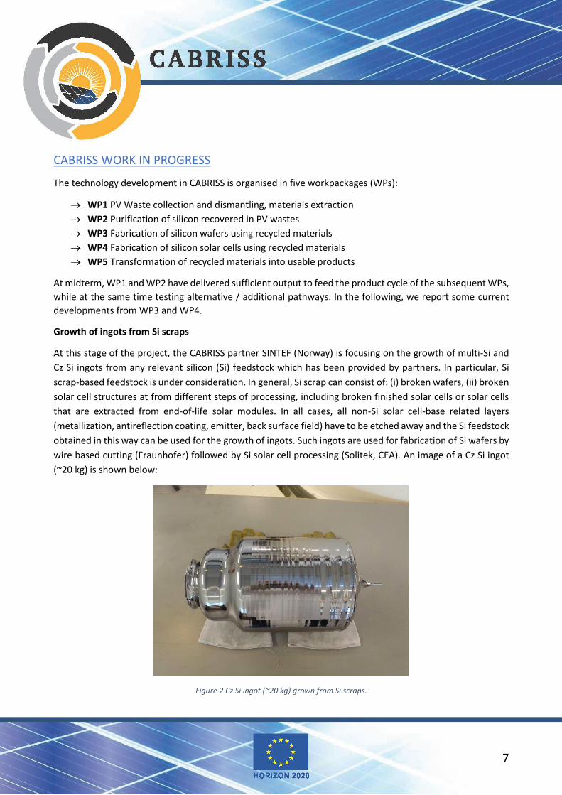
Growth of ingots from Si scraps
At this stage of the project, the CABRISS partner SINTEF (Norway) is focusing on the growth of multi-Si and
Cz Si ingots from any relevant silicon (Si) feedstock which has been provided by partners. In particular, Si
scrap-based feedstock is under consideration. In general, Si scrap can consist of: (i) broken wafers, (ii) broken
solar cell structures at from different steps of processing, including broken finished solar cells or solar cells
that are extracted from end-of-life solar modules. In all cases, all non-Si solar cell-base related layers
(metallization, antireflection coating, emitter, back surface field) have to be etched away and the Si feedstock
obtained in this way can be used for the growth of ingots. Such ingots are used for fabrication of Si wafers by
wire based cutting (Fraunhofer) followed by Si solar cell processing (Solitek, CEA). An image of a Cz Si ingot
(~20 kg) is shown below:
Figure 2 Cz Si ingot (~20 kg) grown from Si scraps.

8
Transformation of Silicon kerf to ingots
The CABRISS partner RHP (Austria) is looking into the transformation of recycled silicon powder into ingots.
As a starting material RHP uses silicon powder that is provided by the project partner RESITEC (Norway). The
silicon powder is available in different particle size and was investigated with respect to the densification
behaviour using a pressure assisted sintering technique such as hot pressing. One of the goals of RHP is to
develop an industrial process which allows a fast transformation of the powders to ingots. To do so, a rapid
hot pressing process was applied and investigated. The silicon powders are inserted into a pressing mold
which is typically made from graphite. One of the issues to solve was to identify suitable processing conditions
that allow to obtain a high densification of >95%. This requires temperatures which are close to the melting
point of silicon. Consequently, appropriate protection layers for the graphite tooling have to be studied.
By applying a rapid hot pressing process heating rates of 50-100 Kelvin per minute can be realized. Therefore,
the cycle for the ingot processing is significant faster compared to conventional hot pressing. An additional
advantage of the used powder metallurgical process is the possibility to tune the electrical conductivity by
using doping of the silicon with elements such as boron. First ingots could be processed with a size of 156
mm x 156 mm. The ingots are now tested for multi-wire cutting and subsequent manufacturing of cells.
Figure 3 Left: Pseudo-square ingot with size of 156 mm X 156 mm. Right: Ingot with a height of > 105 mm could be obtained.
UPCOMING: CABRISS M18 PROGRESS MEETING
The internal Month 18 CABRISS progress meeting will be held from 8th to 9th December 2016 at the
Technische Universität Wien, Austria.

![Impurities and defects in monocrystalline Cz silicon...Figure 20 - Overview of crystal defects in silicon lattice [41] – a – interstitial impurity atom, b – edge dislocation,](https://img.pdfslide.us/doc/110x75/61254e946899e646f32c1b1f/impurities-and-defects-in-monocrystalline-cz-silicon-figure-20-overview-of.jpg)