Embed Size (px)
Citation preview
FN7714Rev.4.00
Jun 7, 2019
ISL976874-Channel LED Driver with Phase Shift Control and 10-Bit Dimming Resolution
DATASHEET
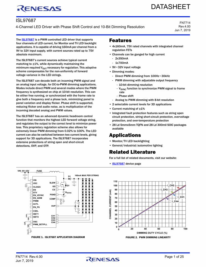
The ISL97687 is a PWM controlled LED driver that supports four channels of LED current, for Monitor and TV LCD backlight applications. It is capable of driving 160mA per channel from a 9V to 32V input supply, with current sources rated up to 75V absolute maximum.
The ISL97687’s current sources achieve typical current matching to ±1%, while dynamically maintaining the minimum required VOUT necessary for regulation. This adaptive scheme compensates for the non-uniformity of forward voltage variance in the LED strings.
The ISL97687 can decode both an incoming PWM signal and an analog input voltage, for DC-to-PWM dimming applications. Modes include direct PWM and several modes where the PWM frequency is synthesized on chip at 10-bit resolution. This can be either free running, or synchronized with the frame rate to give both a frequency and a phase lock, minimizing panel to panel variation and display flicker. Phase shift is supported, reducing flicker and audio noise, as is multiplication of the incoming decoded analog and PWM values.
The ISL97687 has an advanced dynamic headroom control function that monitors the highest LED forward voltage string, and regulates the output to the correct level to minimize power loss. This proprietary regulation scheme also allows for extremely linear PWM dimming from 0.02% to 100%. The LED current can also be switched between two current levels, giving support for 3D applications. The ISL97687 incorporates extensive protections of string open and short-circuit detections, OVP, and OTP.
Features• 4x160mA, 75V rated channels with integrated channel
regulation FETs
• Channels can be ganged for high current - 2x350mA
- 1x700mA
• 9V~32V input voltage
• Dimming modes:
- Direct PWM dimming from 100Hz~30kHz
- PWM dimming with adjustable output frequency
- 10-bit dimming resolution- VSYNC function to synchronize PWM signal to frame
rate- Phase shift
- Analog to PWM dimming with 8-bit resolution
• 2 selectable current levels for 3D applications
• Current matching of ±1%
• Integrated fault protection features such as string open circuit protection, string short-circuit protection, overvoltage protection, and over-temperature protection
• 28 Ld 5mmx5mm TQFN and 28 Ld 300mil SOIC packages available
Applications• Monitor/TV LED backlighting
• General/industrial/automotive lighting
Related LiteratureFor a full list of related documents, visit our website:
• ISL97687 device page
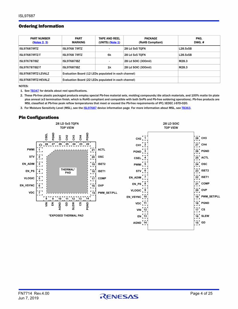
FIGURE 1. ISL97687 APPLICATION DIAGRAM FIGURE 2. PWM DIMMING LINEARITY
PWMI
EN_ADIM
OSC
GD
PWM_SET/PLL
EN
OVP
VIN
STV
VLOGIC
VDC
EN_VSYNC
D1
CS
CH1CH2CH3CH4
CSEL
ISET2
EN_PS
COMP
FUSE
ACTL
PGND
SLEW
VIN: 9V~32V
160mA MAX PER STRING
Q1
RSENSE
ISET1
0
10
20
30
40
50
60
70
80
90
100
110
0 20 40 60 80 100
DIMMING DUTY CYCLE (%)
I_CH2
CH
AN
NE
L C
UR
RE
NT
(m
A)
I_CH1
I_CH3
I_CH4
FN7714 Rev.4.00 Page 1 of 25Jun 7, 2019

ISL97687
Table of ContentsOverview . . . . . . . . . . . . . . . . . . . . . . . . . . . . . . . . . . . . . . . . . . . . . . . . . . . . . . . . . . . . . . . . . . . . . . . . . . . . . . . . . . . . . . . . . . . . . . . . . . . . . . . . . . . 3
Block Diagram . . . . . . . . . . . . . . . . . . . . . . . . . . . . . . . . . . . . . . . . . . . . . . . . . . . . . . . . . . . . . . . . . . . . . . . . . . . . . . . . . . . . . . . . . . . . . . . . . . . .3Ordering Information. . . . . . . . . . . . . . . . . . . . . . . . . . . . . . . . . . . . . . . . . . . . . . . . . . . . . . . . . . . . . . . . . . . . . . . . . . . . . . . . . . . . . . . . . . . . . . .4Pin Configurations . . . . . . . . . . . . . . . . . . . . . . . . . . . . . . . . . . . . . . . . . . . . . . . . . . . . . . . . . . . . . . . . . . . . . . . . . . . . . . . . . . . . . . . . . . . . . . . . .4Pin Descriptions . . . . . . . . . . . . . . . . . . . . . . . . . . . . . . . . . . . . . . . . . . . . . . . . . . . . . . . . . . . . . . . . . . . . . . . . . . . . . . . . . . . . . . . . . . . . . . . . . . .5
Absolute Maximum Ratings . . . . . . . . . . . . . . . . . . . . . . . . . . . . . . . . . . . . . . . . . . . . . . . . . . . . . . . . . . . . . . . . . . . . . . . . . . . . . . . . . . . 6
Thermal Information . . . . . . . . . . . . . . . . . . . . . . . . . . . . . . . . . . . . . . . . . . . . . . . . . . . . . . . . . . . . . . . . . . . . . . . . . . . . . . . . . . . . . . . . . 6
Operating Conditions . . . . . . . . . . . . . . . . . . . . . . . . . . . . . . . . . . . . . . . . . . . . . . . . . . . . . . . . . . . . . . . . . . . . . . . . . . . . . . . . . . . . . . . . 6
Electrical Specifications . . . . . . . . . . . . . . . . . . . . . . . . . . . . . . . . . . . . . . . . . . . . . . . . . . . . . . . . . . . . . . . . . . . . . . . . . . . . . . . . . . . . . 6
Typical Performance Curves. . . . . . . . . . . . . . . . . . . . . . . . . . . . . . . . . . . . . . . . . . . . . . . . . . . . . . . . . . . . . . . . . . . . . . . . . . . . . . . . . . . . . . . . . . . 8
Theory of Operation. . . . . . . . . . . . . . . . . . . . . . . . . . . . . . . . . . . . . . . . . . . . . . . . . . . . . . . . . . . . . . . . . . . . . . . . . . . . . . . . . . . . . . . . . . . . . . . . . 11PWM Boost Converter . . . . . . . . . . . . . . . . . . . . . . . . . . . . . . . . . . . . . . . . . . . . . . . . . . . . . . . . . . . . . . . . . . . . . . . . . . . . . . . . . . . . . . . . . . . . 11OVP and VOUT . . . . . . . . . . . . . . . . . . . . . . . . . . . . . . . . . . . . . . . . . . . . . . . . . . . . . . . . . . . . . . . . . . . . . . . . . . . . . . . . . . . . . . . . . . . . . . . . . . 11Current Matching and Current Accuracy. . . . . . . . . . . . . . . . . . . . . . . . . . . . . . . . . . . . . . . . . . . . . . . . . . . . . . . . . . . . . . . . . . . . . . . . . . . . . 11Dynamic Headroom Control . . . . . . . . . . . . . . . . . . . . . . . . . . . . . . . . . . . . . . . . . . . . . . . . . . . . . . . . . . . . . . . . . . . . . . . . . . . . . . . . . . . . . . . 11Dimming Controls . . . . . . . . . . . . . . . . . . . . . . . . . . . . . . . . . . . . . . . . . . . . . . . . . . . . . . . . . . . . . . . . . . . . . . . . . . . . . . . . . . . . . . . . . . . . . . . 11LED DC Current Setting . . . . . . . . . . . . . . . . . . . . . . . . . . . . . . . . . . . . . . . . . . . . . . . . . . . . . . . . . . . . . . . . . . . . . . . . . . . . . . . . . . . . . . . . . . . 11PWM Dimming Frequency Adjustment. . . . . . . . . . . . . . . . . . . . . . . . . . . . . . . . . . . . . . . . . . . . . . . . . . . . . . . . . . . . . . . . . . . . . . . . . . . . . . 13Phase Shift Control . . . . . . . . . . . . . . . . . . . . . . . . . . . . . . . . . . . . . . . . . . . . . . . . . . . . . . . . . . . . . . . . . . . . . . . . . . . . . . . . . . . . . . . . . . . . . . 13VOUT Control when LEDs are Off. . . . . . . . . . . . . . . . . . . . . . . . . . . . . . . . . . . . . . . . . . . . . . . . . . . . . . . . . . . . . . . . . . . . . . . . . . . . . . . . . . . . 14Switching Frequency . . . . . . . . . . . . . . . . . . . . . . . . . . . . . . . . . . . . . . . . . . . . . . . . . . . . . . . . . . . . . . . . . . . . . . . . . . . . . . . . . . . . . . . . . . . . . 145V and 2.4V Low Dropout Regulators . . . . . . . . . . . . . . . . . . . . . . . . . . . . . . . . . . . . . . . . . . . . . . . . . . . . . . . . . . . . . . . . . . . . . . . . . . . . . . . 14Soft-Start and Boost Current Limit . . . . . . . . . . . . . . . . . . . . . . . . . . . . . . . . . . . . . . . . . . . . . . . . . . . . . . . . . . . . . . . . . . . . . . . . . . . . . . . . . 14Fault Protection and Monitoring . . . . . . . . . . . . . . . . . . . . . . . . . . . . . . . . . . . . . . . . . . . . . . . . . . . . . . . . . . . . . . . . . . . . . . . . . . . . . . . . . . . 14Short-Circuit Protection (SCP) . . . . . . . . . . . . . . . . . . . . . . . . . . . . . . . . . . . . . . . . . . . . . . . . . . . . . . . . . . . . . . . . . . . . . . . . . . . . . . . . . . . . . 15Open Circuit Protection (OCP) . . . . . . . . . . . . . . . . . . . . . . . . . . . . . . . . . . . . . . . . . . . . . . . . . . . . . . . . . . . . . . . . . . . . . . . . . . . . . . . . . . . . . 15Undervoltage Lockout . . . . . . . . . . . . . . . . . . . . . . . . . . . . . . . . . . . . . . . . . . . . . . . . . . . . . . . . . . . . . . . . . . . . . . . . . . . . . . . . . . . . . . . . . . . . 15Over-Temperature Protection (OTP) . . . . . . . . . . . . . . . . . . . . . . . . . . . . . . . . . . . . . . . . . . . . . . . . . . . . . . . . . . . . . . . . . . . . . . . . . . . . . . . . 15Shutdown . . . . . . . . . . . . . . . . . . . . . . . . . . . . . . . . . . . . . . . . . . . . . . . . . . . . . . . . . . . . . . . . . . . . . . . . . . . . . . . . . . . . . . . . . . . . . . . . . . . . . . 15
Component Selections . . . . . . . . . . . . . . . . . . . . . . . . . . . . . . . . . . . . . . . . . . . . . . . . . . . . . . . . . . . . . . . . . . . . . . . . . . . . . . . . . . . . . . . . . . . . . . 16Input Capacitor. . . . . . . . . . . . . . . . . . . . . . . . . . . . . . . . . . . . . . . . . . . . . . . . . . . . . . . . . . . . . . . . . . . . . . . . . . . . . . . . . . . . . . . . . . . . . . . . . . 16Inductor. . . . . . . . . . . . . . . . . . . . . . . . . . . . . . . . . . . . . . . . . . . . . . . . . . . . . . . . . . . . . . . . . . . . . . . . . . . . . . . . . . . . . . . . . . . . . . . . . . . . . . . . 17Output Capacitors . . . . . . . . . . . . . . . . . . . . . . . . . . . . . . . . . . . . . . . . . . . . . . . . . . . . . . . . . . . . . . . . . . . . . . . . . . . . . . . . . . . . . . . . . . . . . . . 17Channel Capacitor . . . . . . . . . . . . . . . . . . . . . . . . . . . . . . . . . . . . . . . . . . . . . . . . . . . . . . . . . . . . . . . . . . . . . . . . . . . . . . . . . . . . . . . . . . . . . . . 17Schottky Diode . . . . . . . . . . . . . . . . . . . . . . . . . . . . . . . . . . . . . . . . . . . . . . . . . . . . . . . . . . . . . . . . . . . . . . . . . . . . . . . . . . . . . . . . . . . . . . . . . . 17High Current Applications . . . . . . . . . . . . . . . . . . . . . . . . . . . . . . . . . . . . . . . . . . . . . . . . . . . . . . . . . . . . . . . . . . . . . . . . . . . . . . . . . . . . . . . . . 17
PCB Layout Considerations . . . . . . . . . . . . . . . . . . . . . . . . . . . . . . . . . . . . . . . . . . . . . . . . . . . . . . . . . . . . . . . . . . . . . . . . . . . . . . . . . . . . . . . . . . 18Two Layers PCB Layout with TQFN Package . . . . . . . . . . . . . . . . . . . . . . . . . . . . . . . . . . . . . . . . . . . . . . . . . . . . . . . . . . . . . . . . . . . . . . . . . 18General Power PAD Design Considerations . . . . . . . . . . . . . . . . . . . . . . . . . . . . . . . . . . . . . . . . . . . . . . . . . . . . . . . . . . . . . . . . . . . . . . . . . . 18One Layer PCB Layout with SOIC Package. . . . . . . . . . . . . . . . . . . . . . . . . . . . . . . . . . . . . . . . . . . . . . . . . . . . . . . . . . . . . . . . . . . . . . . . . . . 18
Equivalent Circuit Diagrams. . . . . . . . . . . . . . . . . . . . . . . . . . . . . . . . . . . . . . . . . . . . . . . . . . . . . . . . . . . . . . . . . . . . . . . . . . . . . . . . . . . . . . . . . . 21
Revision History . . . . . . . . . . . . . . . . . . . . . . . . . . . . . . . . . . . . . . . . . . . . . . . . . . . . . . . . . . . . . . . . . . . . . . . . . . . . . . . . . . . . . . . . . . . . . . . . . . . . 22
Package Outline Drawings . . . . . . . . . . . . . . . . . . . . . . . . . . . . . . . . . . . . . . . . . . . . . . . . . . . . . . . . . . . . . . . . . . . . . . . . . . . . . . . . . . . . . . . . . . . 23
FN7714 Rev.4.00 Page 2 of 25Jun 7, 2019

ISL97687
OverviewBlock Diagram
FIGURE 3. ISL97687 BLOCK DIAGRAM
REFGEN
VIN
GMAMP
COMP
+-
CH1
CH4
LOGICFET
DRIVERS
OVP
REG1
OSC & RAMP COMP
IMAXILIMIT
FAULT/STATUSREGISTER
HIGHEST VF STRING DETECT
VDC
TEMPSENSOR
PWM_SET/PLL
OSC
EN_PS
ISET1
+-
GND
O/P SHORT
REF_OVPREF_VSC
ANALOG BIAS
+-
OPEN CKT, SHORT CKT DETECTS
1
FAULT/STATUS CONTROL
OVP
4
VSET
FSWOSC
STV
PWMI
LEDDIMMING
CONTROLLER
EN
23
DIGITAL BIASVLOGIC
160mA MAX PER STRING
ISET2
CSEL
GD CS
VIN: 9V~32V
EN_VSYNC
SLEW
FUSE
OVP
ACTL
SERIAL INTERFACE
ANALOG INTERFACE
EN_ADIM
PLL
REG2
= 0
FN7714 Rev.4.00 Page 3 of 25Jun 7, 2019
ISL97687
Ordering Information
Pin Configurations
PART NUMBER(Notes 2, 3)
PART MARKING
TAPE AND REEL(UNITS) (Note 1)
PACKAGE(RoHS Compliant)
PKG.DWG. #
ISL97687IRTZ ISL9768 7IRTZ - 28 Ld 5x5 TQFN L28.5x5B
ISL97687IRTZ-T ISL9768 7IRTZ 6k 28 Ld 5x5 TQFN L28.5x5B
ISL976787IBZ ISL97687IBZ - 28 Ld SOIC (300mil) M28.3
ISL976787IBZ-T ISL97687IBZ 1k 28 Ld SOIC (300mil) M28.3
ISL97687IRTZ-LEVALZ Evaluation Board (12 LEDs populated in each channel)
ISL97687IRTZ-HEVALZ Evaluation Board (22 LEDs populated in each channel)
NOTES:
1. See TB347 for details about reel specifications.
2. These Pb-free plastic packaged products employ special Pb-free material sets, molding compounds/die attach materials, and 100% matte tin plate plus anneal (e3 termination finish, which is RoHS compliant and compatible with both SnPb and Pb-free soldering operations). Pb-free products are MSL classified at Pb-free peak reflow temperatures that meet or exceed the Pb-free requirements of IPC/JEDEC J-STD-020.
3. For Moisture Sensitivity Level (MSL), see the ISL97687 device information page. For more information about MSL, see TB363.
28 LD 5x5 TQFNTOP VIEW
28 LD SOICTOP VIEW
PG
ND
CH
1
CH
2
CH
3
CH
4
PG
ND
VIN EN
AG
ND
GD
SL
EW CS
PWMI
STV
EN_ADIM
EN_PS
VLOGIC
EN_VSYNC
VDC
ACTL
OSC
ISET2
ISET1
COMP
OVP
1
2
3
4
5
6
7
21
20
19
18
17
16
8 9 10 11 12 13
THERMAL* PAD
PWM_SET/PLL15
14
PG
ND
28 27 26 25 24 23 22
CS
EL
*EXPOSED THERMAL PAD
1
2
3
4
5
6
7
8
9
10
11
12
13
14
28
27
26
25
24
23
22
21
20
19
18
17
16
15
CH2
EN_ADIM
EN_PS
VLOGIC
ISET2
ISET1
CH1
PGND
CSEL
PWMI
STV
EN_VSYNC
VDC
VIN
EN
AGND GD
SLEW
CS
PGND
PWM_SET/PLL
OVP
COMP
OSC
ACTL
PGND
CH4
CH3
FN7714 Rev.4.00 Page 4 of 25Jun 7, 2019
ISL97687
Pin Descriptions
TQFN SOIC PIN NAME PIN TYPE PIN DESCRIPTION
1 5 PWMI I PWM brightness control input pin
2 6 STV I Start vertical frame signal; used in VSYNC mode
3 7 EN_ADIM I Enable analog dimming
4 8 EN_PS I Enable phase shift
5 9 VLOGIC S Internal 2.5V digital bias regulator. Needs decoupling capacitor added to ground.
6 10 EN_VSYNC I Frame synchronization enable. Ties high to VDC for enable VSYNC function. PWM_SET/PLL also needs to be configured with an RC network. Pin can be tied to VDC or VLOGIC to enable function.
7 11 VDC S Internal 5V analog bias regulator. Needs decoupling capacitor added to ground.
8 12 VIN S Main power input. Range: 9V to 32V.
9 13 EN I LED driver enable. The whole chip shuts down when low.
10 14 AGND S Analog ground
11 15 GD O External boost FET gate control
12 16 SLEW I Boost regulation switching slew rate control
13 17 CS I External boost FET current sense input
14 18 PGND S Boost FET gate driver power ground and ground reference for the CS pin.
15 19 PWM_SET/PLL
I For direct PWM mode, tie this pin high to VDC. For other non-VSYNC modes, connect to a resistor to set the dimming frequency. If the VSYNC function is enabled, connect this pin to the PLL loop filter network.
16 20 OVP I Overvoltage protection input and output voltage feedback pin.
17 21 COMP I Boost compensation
18 22 ISET1 I Resistor connection for setting LED current. 28.7kΩ = 100mA.
19 23 ISET2 I Resistor connection for setting LED current. 28.7kΩ = 100mA.
20 24 OSC I Boost switching frequency adjustment.
21 25 ACTL I Analog dimming input (input range is 0.3V to 3V).
22 26 PGND S Power Ground return for LED current.
23 27 CH4 I LED PWM driver
24 28 CH3 I LED PWM driver
25 1 CH2 I LED PWM driver
26 2 CH1 I LED PWM driver
27 3 PGND S Power ground return for LED current.
28 4 CSEL I ISET resistor selection pin. CSEL = 0 : ISET 1 resistor sets LED currentCSEL = 1 : ISET 2 resistor sets LED current
FN7714 Rev.4.00 Page 5 of 25Jun 7, 2019

ISL97687
Absolute Maximum Ratings (TA = +25°C) Thermal InformationVIN, EN, PWMI, ACTL . . . . . . . . . . . . . . . . . . . . . . . . . . . . . . . . . . -0.3V to 45VVDC. . . . . . . . . . . . . . . . . . . . . . . . . . . . . . . . . . . . . . . . . . . . . . . -0.3V to 5.75VVLOGIC . . . . . . . . . . . . . . . . . . . . . . . . . . . . . . . . . . . . . . . . . . . . -0.3V to 2.75VCOMP, ISET1, ISET2, PWM_SET,
OSC, CS, OVP. . . . . . . . . . . . . . . . . . . . . . .-0.3V to min (VDC+0.3V, 5.75V)EN_VSYNC, CSEL. . . . . . . . . . . . . . . . . . . . . . . . . . . . . . . . . . . . -0.3V to 5.75VSTV, EN_ADIM, EN_PS . . . . . . . . . . . . . . . . . . . . . . . . . . . . . . . -0.3V to 5.75VCH1 - CH4 . . . . . . . . . . . . . . . . . . . . . . . . . . . . . . . . . . . . . . . . . . . -0.3V to 75VGD, SLEW. . . . . . . . . . . . . . . . . . . . . . . . . . . . . . . . . . . . . . . . . . . . -0.3V to 18VPGND . . . . . . . . . . . . . . . . . . . . . . . . . . . . . . . . . . . . . . . . . . . . . -0.3V to +0.3VAbove voltage ratings are all with respect to AGND pin
ESD RatingHuman Body Model (Tested per JESD22-A114F) . . . . . . . . . . . . . . . . 2kVMachine Model (Tested per JESD22-A115C) . . . . . . . . . . . . . . . . . . 200VCharged Device Model (JESD22-C101E) . . . . . . . . . . . . . . . . . . . . . . . 1kV
Latch Up (Tested per JESD-78B; Class 2, Level A) . . . . . . . . . . . . . . 100mA
Thermal Resistance JA (°C/W) JC (°C/W)28 Ld TQFN (4 layer + vias, Notes 4, 5) . . . 32 428 Ld SOIC (4 layer, Notes 6, 7) . . . . . . . . . 54 25
Thermal Characterization (Typical, Note 8) PSIJT (°C/W)
28 Ld TQFN . . . . . . . . . . . . . . . . . . . . . . . . . . . . . . . . . . . . 128 Ld SOIC. . . . . . . . . . . . . . . . . . . . . . . . . . . . . . . . . . . . . 4
Maximum Continuous Junction Temperature . . . . . . . . . . . . . . . . .+125°CStorage Temperature . . . . . . . . . . . . . . . . . . . . . . . . . . . . .-65°C to +150°CPower Dissipation TQFN (W) SOIC (W)TA < +25°C . . . . . . . . . . . . . . . . . . . . . . . . . . . . 3.13 1.85TA < +70°C . . . . . . . . . . . . . . . . . . . . . . . . . . . . 1.72 1.02TA < +85°C . . . . . . . . . . . . . . . . . . . . . . . . . . . . 1.25 0.74TA < +105°C . . . . . . . . . . . . . . . . . . . . . . . . . . . 0.63 0.37Pb-Free Reflow Profile . . . . . . . . . . . . . . . . . . . . . . . . . . . . . . . . . . see TB493
Operating ConditionsTemperature Range . . . . . . . . . . . . . . . . . . . . . . . . . . . . . . .-40°C to +105°C
CAUTION: Do not operate at or near the maximum ratings listed for extended periods of time. Exposure to such conditions can adversely impact productreliability and result in failures not covered by warranty.
NOTES:
4. JA is measured in free air with the component mounted on a high-effective thermal conductivity test board with “direct attach” features. See TB379.
5. For JC, the “case temp” location is the center of the exposed metal pad on the package underside.
6. For JC, the “case temp” location is taken at the package top center.
7. JA is measured with the component mounted on a high-effective thermal conductivity test board in free air. See TB379 for details.
8. PSIJT is the PSI junction-to-top thermal characterization parameter. If the package top temperature can be measured with this rating then the die junction temperature can be estimated more accurately than the JC and JC thermal resistance ratings.
Electrical Specifications All specifications below are characterized at TA = -40°C to +105°C; VIN = 12V, EN = 5V. Boldface limits apply across the operating temperature range, -40°C to +105°C.
PARAMETER SYMBOL CONDITIONMIN
(Note 9) TYPMAX
(Note 9) UNIT
GENERAL
Backlight Supply Voltage VIN (Note 10) 9 32 V
VIN Shutdown Current IVIN_STBY EN = 0 5 µA
Switching IVIN_ACTIVE RFPWM = 3.3kΩ,ILED = 100mA,fSW = 600kHz,COUT_SW = 1nF
10 13 mA
Non-Switching 4 5.5 mA
Undervoltage Lockout Threshold VUVLO 2.9 3.3 V
Undervoltage Lockout Hysteresis VUVLO_HYS 300 mV
LINEAR REGULATOR
5V Analog Bias Regulator VDC VIN > 6V 4.8 5 5.1 V
VDC LDO Load Regulation Tolerance VDC_DROP IVDC = 30mA 71 100 mV
2.5V Logic Bias Regulator VLOGIC VIN > 6V 2.3 2.4 2.5 V
VLOGIC LDO Load Regulation Tolerance VLOGIC_DROP IVLOGIC = 30mA 31 100 mV
BOOST SWITCH CONTROLLER
Soft-Start tSS 16 ms
Boost FET Current Limit (See Equation 5) ISW_LIMIT RSENSE = 50mΩ 3.1 3.4 3.8 A
Gate Rise Time tR COUT_SW = 1000pF 20 ns
Gate Falling Time tF COUT_SW = 1000pF 17.6 ns
Gate Driver Output Voltage VGD COUT_SW = 1000pF 10 V
FN7714 Rev.4.00 Page 6 of 25Jun 7, 2019

ISL97687
Boost Maximum Duty Cycle DMAX fSW = 600kHz 92 %
Boost Minimum Duty Cycle DMIN fSW = 1.2MHz 26 %
Boost Switching Frequency (See Equation 4) fSW ROSC = 250kΩ 180 200 220 kHz
ROSC = 83kΩ 540 600 660 kHz
ROSC = 42kΩ 1.08 1.2 1.32 MHz
Boost Peak Efficiency EFFPEAK 90 %
REFERENCE
Channel-to-Channel Current Matching IMATCH Channels are in a single IC, ILED: 100mA
-2 ±1 2 %
Absolute Current IACC RISET1/2 = 28.7kΩ -3 3 %
FAULT DETECTION
Channel Short-Circuit Threshold VSC 7.2 8 8.8 V
Over-Temperature Threshold VTEMP 150 °C
Over-Temperature Threshold Accuracy VTEMP_ACC 5 °C
Overvoltage Limit on OVP Pin VOVP_OUT 1.18 1.22 1.24 V
Overvoltage Limit on VIN Pin VOVP_IN 35 V
DIGITAL I/O LOGIC LEVEL SPECIFICATIONS
Logic Input Low Voltage - STV, EN_PS, EN_VSYNC, EN_ADIM, PWMI, CSEL, EN
VIL 0.8 V
Logic Input High Voltage - STV, EN_PS, EN_VSYNC, EN_ADIM, PWMI, CSEL, EN
VIH 1.5 5.5 V
Frame Frequency STV 30 240 Hz
CURRENT SOURCES
Dominant Channel Current Source Headroom at CH Pin VHEADROOM ILED = 160mATA = +25°C
0.75(Note 11)
V
Dominant Channel Current Sink Headroom Range at CHx Pin
VHEADROOM_RANGE ILED = 20mA,TA = +25°C
90 mV
Voltage at ISET1 and 2 Pins VISET1,2 1.18 1.21 1.24 V
Maximum LED Current per Channel ILED_MAX 160 mA
PWM GENERATOR
Generated PWM Frequency (See Equation 3) fPWM RPWM_SET = 333kΩ 45 50 55 Hz
RPWM_SET = 3.3kΩ 4.5 5 5.5 kHz
PWM Dimming Duty Cycle Limits Dimming Range fPWM ≤ 20kHz 0.1 100 %
PWMI Input Frequency Range fPWMI 60 20k Hz
PWM_SET Voltage VPWM_SET RPWM_SET = 3.3kΩ 1.18 1.21 1.25 V
Analog Dimming Input VACTL 0% Dimming 0.28 0.3 0.31 V
100% Dimming 2.95 3 3.1 V
Minimum PWM On-Time in Direct PWM Mode tPWM_MIN 350 ns
NOTES:
9. Parameters with MIN and/or MAX limits are 100% tested at +25°C, unless otherwise specified. Temperature limits established by characterization and are not production tested.
10. At maximum VIN of 32V, minimum VOUT is 35V. Minimum VOUT can be lower at lower VIN.
11. Varies within the range specified by VHEADROOM_RANGE.
Electrical Specifications All specifications below are characterized at TA = -40°C to +105°C; VIN = 12V, EN = 5V. Boldface limits apply across the operating temperature range, -40°C to +105°C. (Continued)
PARAMETER SYMBOL CONDITIONMIN
(Note 9) TYPMAX
(Note 9) UNIT
FN7714 Rev.4.00 Page 7 of 25Jun 7, 2019
ISL97687
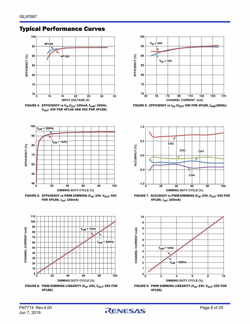
Typical Performance Curves
FIGURE 4. EFFICIENCY vs VIN (ICH: 100mA, fDIM: 200Hz, VOUT: 45V FOR 4P14S AND 55V FOR 4P18S)
FIGURE 5. EFFICIENCY vs ICH (VOUT: 55V FOR 4P18S, fDIM:200Hz)
FIGURE 6. EFFICIENCY vs PWM DIMMING (VIN: 24V, VOUT: 55V FOR 4P18S, ICH: 100mA)
FIGURE 7. ACCURACY vs PWM DIMMING (VIN: 24V, VOUT: 55V FOR 4P18S, ICH: 100mA)
FIGURE 8. PWM DIMMING LINEARITY (VIN: 24V, VOUT: 55V FOR 4P18S)
FIGURE 9. PWM DIMMING LINEARITY (VIN: 24V, VOUT: 55V FOR 4P18S)
70
75
80
85
90
95
100
5 10 15 20 25 30 35INPUT VOLTAGE (V)
EF
FIC
IEN
CY
(%
)
4P18S
4P14S
70
75
80
85
90
95
100
30 50 70 90 110 130 150 170
CHANNEL CURRENT (mA)
EF
FIC
IEN
CY
(%
)
VIN = 24V
VIN = 19V
40
50
60
70
80
90
100
0 20 40 60 80 100
DIMMING DUTY CYCLE (%)
EF
FIC
IEN
CY
(%
)
fDIM = 1kHz
fDIM = 200Hz
-1.0
-0.5
0.0
0.5
1.0
0 20 40 60 80 100
AC
CU
RA
CY
(%
)
DIMMING DUTY CYCLE (%)
CH2
CH1CH3
CH4
0
10
20
30
40
50
60
70
80
90
100
110
0 20 40 60 80 100
DIMMING DUTY CYCLE (%)
CH
AN
NE
L C
UR
RE
NT
(m
A)
fDIM = 1kHz
fDIM = 200Hz
0
1
2
3
4
5
6
7
8
9
10
0 2 4 6 8 10
DIMMING DUTY CYCLE (%)
CH
AN
NE
L C
UR
RE
NT
(m
A)
fDIM = 1kHz
fDIM = 200Hz
FN7714 Rev.4.00 Page 8 of 25Jun 7, 2019

ISL97687
FIGURE 10. START-UP (DIRECT PWM DIMMING, VIN: 19V, ICH: 120mA, LEDs: 4P18S, fDIM: 200Hz)
FIGURE 11. DIRECT PWM DIMMING (VIN: 19V, LEDs: 4P18S, fDIM: 200Hz)
FIGURE 12. START-UP WITHOUT PHASE SHIFT (VIN : 19V, ICH: 120mA, LEDs: 4P18S, fDIM: 200Hz)
FIGURE 13. START-UP WITH PHASE SHIFT (VIN : 19V, ICH: 120mA, LEDs: 4P18S, fDIM: 200Hz)
FIGURE 14. PWM DIMMING WITHOUT PHASE SHIFT (VIN: 19V, ICH: 120mA, LEDs: 4P18S, fDIM: 200Hz)
FIGURE 15. PWM DIMMING WITH PHASE SHIFT (VIN: 19V, ICH: 120mA, LEDs: 4P18S, fDIM: 200Hz)
Typical Performance Curves (Continued)
I_INDUCTOR
V_OUT
V_CH
I_CH
V_PWMI
V_LX
V_CH1
I_CH2
I_INDUCTOR
V_CH2
I_CH1
V_OUT
I_INDUCTOR
V_CH2
I_CH1
V_OUT
I_INDUCTOR
V_CH1
I_CH2
I_INDUCTOR
V_CH1
I_CH2
FN7714 Rev.4.00 Page 9 of 25Jun 7, 2019
ISL97687
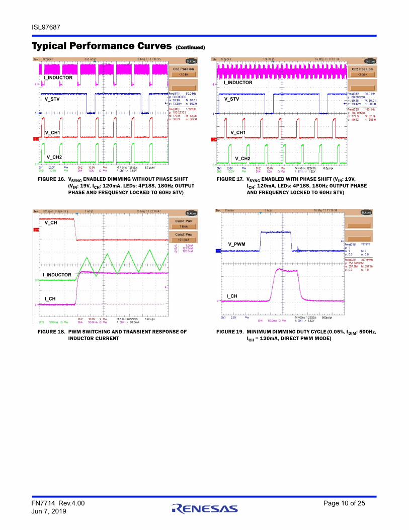
FIGURE 16. VSYNC ENABLED DIMMING WITHOUT PHASE SHIFT (VIN: 19V, ICH: 120mA, LEDs: 4P18S, 180Hz OUTPUT PHASE AND FREQUENCY LOCKED TO 60Hz STV)
FIGURE 17. VSYNC ENABLED WITH PHASE SHIFT (VIN: 19V, ICH: 120mA, LEDs: 4P18S, 180Hz OUTPUT PHASE AND FREQUENCY LOCKED TO 60Hz STV)
FIGURE 18. PWM SWITCHING AND TRANSIENT RESPONSE OF INDUCTOR CURRENT
FIGURE 19. MINIMUM DIMMING DUTY CYCLE (0.05%, fDIM: 500Hz, ICH = 120mA, DIRECT PWM MODE)
Typical Performance Curves (Continued)
I_INDUCTOR
V_CH2
V_CH1
V_STV
I_INDUCTOR
V_CH2
V_CH1
V_STV
I_INDUCTOR
V_CH
I_CH
V_PWM
I_CH
FN7714 Rev.4.00 Page 10 of 25Jun 7, 2019
ISL97687
Theory of OperationPWM Boost ConverterThe current mode PWM boost converter produces the minimal voltage needed to enable the LED string with the highest forward voltage drop to run at the programmed current. The ISL97687 employs current mode control boost architecture that has a fast current sense loop and a slow voltage feedback loop. The number of LEDs that can be driven by ISL97687 depends on the type of LED chosen in the application. The ISL97687 is capable of boosting up to greater than 70V and driving 4 Channels of LEDs at a maximum of 160mA per channel.
OVP and VOUT The Overvoltage Protection (OVP) pin has a function of setting the overvoltage trip level and limiting the VOUT regulation range.
The ISL97687 OVP threshold is set by RUPPER and RLOWER as shown in Equation 1:
and VOUT can only regulate between 30% and 100% of the VOUT_OVP such that:
Allowable VOUT = 30% to 100% of VOUT_OVP
For example, a 1MΩ RUPPER and 19kΩ RLOWER sets OVP to 65.9V. The boost can regulate down to 30% of OVP, so it can go as low as 19.5V. If VOUT needs to be lower than this, the OVP level must be reduced. Otherwise, VOUT regulates to 19.5V, and the ISL97687 may overheat. However, it’s recommended that the OVP be set to no more than 20% above the nominal operating voltage. This prevents the need for output capacitor voltage ratings and the inductor current rating to be set significantly higher than needed under normal conditions, allowing a smaller and cheaper solution, and keeping the maximum voltages and currents that can be seen in the system during fault conditions at less extreme levels.
Place parallel capacitors across the OVP resistors such that RUPPER /RLOWER = CLOWER /CUPPER. Using a CUPPER value of at least 30pF is recommended. These capacitors reduce the AC impedance of the OVP node, which is important when using high value resistors. The ratio of the OVP capacitors should be the inverse of the OVP resistors. For example, if RUPPER/RLOWER = 33/1, CUPPER /C LOWER = 1/33 with CUPPER = 100pF and CLOWER = 3.3nF. These components are not always needed, but it is highly recommended to include placeholders.
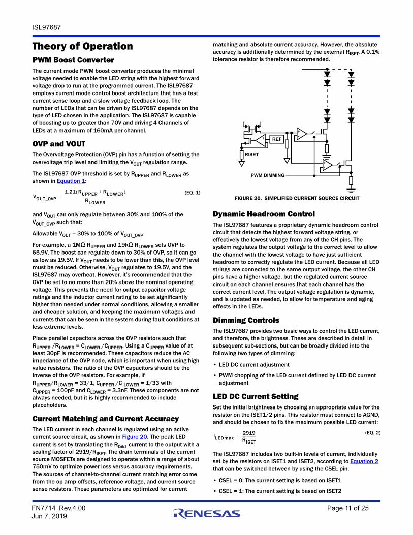
Current Matching and Current AccuracyThe LED current in each channel is regulated using an active current source circuit, as shown in Figure 20. The peak LED current is set by translating the RISET current to the output with a scaling factor of 2919/RISET. The drain terminals of the current source MOSFETs are designed to operate within a range of about 750mV to optimize power loss versus accuracy requirements. The sources of channel-to-channel current matching error come from the op amp offsets, reference voltage, and current source sense resistors. These parameters are optimized for current
matching and absolute current accuracy. However, the absolute accuracy is additionally determined by the external RISET. A 0.1% tolerance resistor is therefore recommended.
Dynamic Headroom ControlThe ISL97687 features a proprietary dynamic headroom control circuit that detects the highest forward voltage string, or effectively the lowest voltage from any of the CH pins. The system regulates the output voltage to the correct level to allow the channel with the lowest voltage to have just sufficient headroom to correctly regulate the LED current. Because all LED strings are connected to the same output voltage, the other CH pins have a higher voltage, but the regulated current source circuit on each channel ensures that each channel has the correct current level. The output voltage regulation is dynamic, and is updated as needed, to allow for temperature and aging effects in the LEDs.
Dimming ControlsThe ISL97687 provides two basic ways to control the LED current, and therefore, the brightness. These are described in detail in subsequent sub-sections, but can be broadly divided into the following two types of dimming:
• LED DC current adjustment
• PWM chopping of the LED current defined by LED DC current adjustment
LED DC Current SettingSet the initial brightness by choosing an appropriate value for the resistor on the ISET1/2 pins. This resistor must connect to AGND, and should be chosen to fix the maximum possible LED current:
The ISL97687 includes two built-in levels of current, individually set by the resistors on ISET1 and ISET2, according to Equation 2 that can be switched between by using the CSEL pin.
• CSEL = 0: The current setting is based on ISET1
• CSEL = 1: The current setting is based on ISET2
VOUT_OVP
1.21 RUPPER RLOWER+
RLOWER-------------------------------------------------------------------=
(EQ. 1)FIGURE 20. SIMPLIFIED CURRENT SOURCE CIRCUIT
+-
+-
REF
RISET
PWM DIMMING
+-
ILEDmax2919RISET---------------=
(EQ. 2)
FN7714 Rev.4.00 Page 11 of 25Jun 7, 2019
ISL97687
This is typically used in 3D systems to provide a higher current level in 3D modes, but is not restricted to this application. CSEL can be switched in operation and updates immediately in direct PWM mode, and at the start of the next PWM dimming cycle in other modes. The different current levels need to be close enough so that the change in output voltages (VOUT) are within 2.3% of VOUT_OVP.
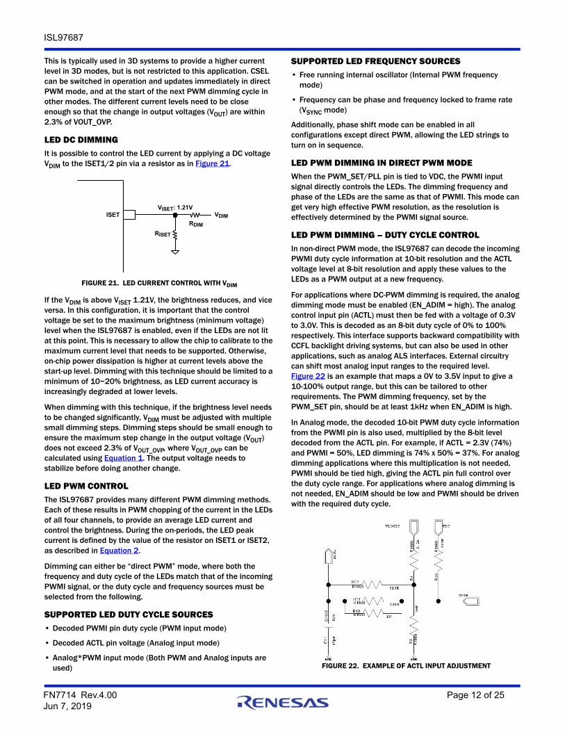
LED DC DIMMINGIt is possible to control the LED current by applying a DC voltage VDIM to the ISET1/2 pin via a resistor as in Figure 21.
If the VDIM is above VISET 1.21V, the brightness reduces, and vice versa. In this configuration, it is important that the control voltage be set to the maximum brightness (minimum voltage) level when the ISL97687 is enabled, even if the LEDs are not lit at this point. This is necessary to allow the chip to calibrate to the maximum current level that needs to be supported. Otherwise, on-chip power dissipation is higher at current levels above the start-up level. Dimming with this technique should be limited to a minimum of 10~20% brightness, as LED current accuracy is increasingly degraded at lower levels.
When dimming with this technique, if the brightness level needs to be changed significantly, VDIM must be adjusted with multiple small dimming steps. Dimming steps should be small enough to ensure the maximum step change in the output voltage (VOUT) does not exceed 2.3% of VOUT_OVP, where VOUT_OVP can be calculated using Equation 1. The output voltage needs to stabilize before doing another change.
LED PWM CONTROLThe ISL97687 provides many different PWM dimming methods. Each of these results in PWM chopping of the current in the LEDs of all four channels, to provide an average LED current and control the brightness. During the on-periods, the LED peak current is defined by the value of the resistor on ISET1 or ISET2, as described in Equation 2.
Dimming can either be “direct PWM” mode, where both the frequency and duty cycle of the LEDs match that of the incoming PWMI signal, or the duty cycle and frequency sources must be selected from the following.
SUPPORTED LED DUTY CYCLE SOURCES• Decoded PWMI pin duty cycle (PWM input mode)
• Decoded ACTL pin voltage (Analog input mode)
• Analog*PWM input mode (Both PWM and Analog inputs are used)
SUPPORTED LED FREQUENCY SOURCES• Free running internal oscillator (Internal PWM frequency
mode)
• Frequency can be phase and frequency locked to frame rate (VSYNC mode)
Additionally, phase shift mode can be enabled in all configurations except direct PWM, allowing the LED strings to turn on in sequence.
LED PWM DIMMING IN DIRECT PWM MODEWhen the PWM_SET/PLL pin is tied to VDC, the PWMI input signal directly controls the LEDs. The dimming frequency and phase of the LEDs are the same as that of PWMI. This mode can get very high effective PWM resolution, as the resolution is effectively determined by the PWMI signal source.
LED PWM DIMMING – DUTY CYCLE CONTROLIn non-direct PWM mode, the ISL97687 can decode the incoming PWMI duty cycle information at 10-bit resolution and the ACTL voltage level at 8-bit resolution and apply these values to the LEDs as a PWM output at a new frequency.
For applications where DC-PWM dimming is required, the analog dimming mode must be enabled (EN_ADIM = high). The analog control input pin (ACTL) must then be fed with a voltage of 0.3V to 3.0V. This is decoded as an 8-bit duty cycle of 0% to 100% respectively. This interface supports backward compatibility with CCFL backlight driving systems, but can also be used in other applications, such as analog ALS interfaces. External circuitry can shift most analog input ranges to the required level. Figure 22 is an example that maps a 0V to 3.5V input to give a 10-100% output range, but this can be tailored to other requirements. The PWM dimming frequency, set by the PWM_SET pin, should be at least 1kHz when EN_ADIM is high.
In Analog mode, the decoded 10-bit PWM duty cycle information from the PWMI pin is also used, multiplied by the 8-bit level decoded from the ACTL pin. For example, if ACTL = 2.3V (74%) and PWMI = 50%, LED dimming is 74% x 50% = 37%. For analog dimming applications where this multiplication is not needed, PWMI should be tied high, giving the ACTL pin full control over the duty cycle range. For applications where analog dimming is not needed, EN_ADIM should be low and PWMI should be driven with the required duty cycle.
FIGURE 21. LED CURRENT CONTROL WITH VDIM
RISET
ISET VDIM
VISET: 1.21V
RDIM
FIGURE 22. EXAMPLE OF ACTL INPUT ADJUSTMENT
FN7714 Rev.4.00 Page 12 of 25Jun 7, 2019

ISL97687
PWM Dimming Frequency AdjustmentThe dimming frequencies of serial interface and ACTL modes are set by an external resistor at the PWM_SET pin, as shown in Equation 3:
where fPWM is the desirable PWM dimming frequency and RPWMSET is the setting resistor.
VSYNC FUNCTIONThe VSYNC function provides accurate LED dimming frequencies and makes sure that the video data is properly aligned with the frame rate. A Phase Locked Loop (PLL) locks the frequency to a multiple of the frame rate. Additionally, the phase of the PWM output is aligned with the frame rate to provide very predictable video performance. In VSYNC mode, the PWM_SET/PLL pin is used as the PLL loop compensation pin and needs a loop filter connected between it and ground.
Frame rates between 30Hz and 300Hz are supported, and an automatic frequency detection circuit provides the same output frequency at 30, 60, 120, 180, 240, and 300Hz.
Additionally, the PWM dimming frequency can be pre-selected to any of the following values shown in Table 1 (Note: For the 60Hz range, the frequencies are scaled by a factor of framerate/60Hz and for the 120Hz range are be scaled by a factor of framerate/120Hz).
Phase Shift ControlThe ISL97687 is capable of delaying the phase of each current source within the PWM cycle. Conventional LED drivers present the worst load transients to the boost converter, by turning on all channels simultaneously, as shown in Figure 23. The ISL97687 can be configured to phase shift each channel by 90°, individually turning them on and off at different points during the PWM dimming period, as shown in Figure 24. At duty cycles below 100%, the load presented to the boost peaks at a lower level and/or spends less time at the peak, when compared to that of a conventional LED driver, as shown in Figure 23. Additionally, load steps are limited to the LED current of one CH pin, one quarter of that of a standard driver. This can help reduce transients on VOUT and also reduces audio noise by limiting the magnitude of changes in magnetic field required in the inductor needed to track the load. Audio noise is also generally improved for PWM frequencies in the audio band, as the effective frequency of the boost load is multiplied by a factor of 4, meaning that, for example, a 5kHz LED frequency offers an effective boost load frequency of 20kHz.
TABLE 1. PRE-SELECTED PWM DIMMING FREQUENCY AT VSYNC MODE
DIMMING FREQUENCY
(Hz) (kHz) (kHz) (kHz)
180 1.26 5.70 13.38
240 1.38 6.18 13.86
300 1.50 6.66 14.34
360 1.62 7.14 14.82
420 1.74 7.62 15.30
480 1.86 8.10 15.78
540 1.98 8.58 16.26
600 2.10 9.06 16.74
660 2.34 9.54 17.22
720 2.58 10.02 17.70
780 2.88 10.50 18.18
840 3.36 10.98 18.66
900 3.78 11.46 19.14
960 4.20 11.94 19.62
1.02k 4.74 12.42 20.10
1.14k 5.22 12.90 20.58
fPWM1.665 710RPWMSET
---------------------------------= (EQ. 3)
FIGURE 23. NON PHASE SHIFT PWM DIMMING AT 50% DUTY CYCLE
FIGURE 24. PHASE SHIFT PWM DIMMING AT 50% DUTY CYCLE
ICH4
ICH_TOTAL
TIME
ICH3
ICH2
ICH1
ICH4
ICH_TOTAL
TIME
ICH3
ICH2
ICH1
FN7714 Rev.4.00 Page 13 of 25Jun 7, 2019
ISL97687
VOUT Control when LEDs are Off When the backlight is enabled but all LEDs are off (such as during the PWM off times), the switching regulator of a typical LED driver stops switching, which can allow the output to begin to discharge.
This is not a problem when the LED off times are short and the duty cycle is running at a high duty cycle, or the output capacitance is large. However, it presents two problems. First, for low duty cycles at low frequencies, VOUT can droop between on-times, resulting in under-regulation of the current when the LEDs are next switched on. Second, at high PWM frequencies or very low duty cycles, LED on-times can be shorter than the minimum number of boost cycles needed to ramp up the inductor current to the required level to support the load. For example, a 1% on-time while running at 20kHz PWM dimming frequency is only 500ns. If the boost switching frequency is set at 500kHz, this only represents a quarter of a switching cycle per LED on-time, which may not be sufficient to ramp the inductor current to the required level.
The ISL97687 incorporates an additional PFM switching mechanism that allows the boost stage to continue to switch at low current levels to replace the energy lost from the output capacitor due to the OVP stack resistance and capacitor self discharge. For very short pulses, this also means that the charge delivered to the LEDs in the on-times is provided entirely by the output capacitor, kept at the correct voltage by the PFM mode in the off-times. This allows the output to always remain very close to the required level, so that when the LEDs are re-enabled, the boost output is already at the correct level. This dramatically improves LED PWM performance, providing industry leading linearity down to sub 1% levels, and reduces the overshoot in the boost inductor current, caused by transient switching when the LEDs are switched on, to a minimum level.
The system continues to maintain VOUT at the target level for 120ms after the last time the LEDs were on. If all LEDs are off for a longer period than this, the converter stops switching and goes into a sleep mode, allowing VOUT to decay to save power during long backlight-off periods.
Switching FrequencyThe boost switching frequency can be adjusted by the resistor on the OSC pin, which must be connected to AGND, and follows Equation 4:
where fSW is the desirable boost switching frequency and ROSC is the setting resistor.
5V and 2.4V Low Dropout RegulatorsA 5V LDO regulator provides the low voltage supply needed to drive internal circuits. The output of this LDO is the VDC pin. A decoupling capacitor of 1µF or more is required between this pin and AGND for correct operation. Similarly, a 2.4V LDO regulator is present at the VLOGIC pin, and also requires a 1µF decoupling capacitor. Both pins can be used as a coarse voltage reference, or as a supply for other circuits, but can only support a load of up to
~10mA and should not be used to power noisy circuits that can feed significant noise onto their supply.
Soft-Start and Boost Current LimitThe boost current limit should be set by using a resistor from CS to PGND. The typical current limit can be calculated as:
The CS resistor should be chosen based on the maximum load that needs to be driven. Typically, a limit of 30~40% more than is required under DC conditions is sufficient to allow for necessary overshoots during load transients. Values of 20~100mΩ are supported.
It is important that PGND pin 14 (QFN)/18 (SOIC) is connected directly to the base of the sense resistor, with no other connection to the ground system, except via this path. This is because this pin is used as a ground reference for the CS pin. Connecting it here gives the maximum noise immunity and the best stability characteristics.
The ISL97687 uses a digital current limit based soft start. The initial limit level is set to one ninth of the full current limit, with eight subsequent steps increasing this by a ninth of the final value every 2ms until it reaches the full limit. In the event that no LEDs have been conducting during the interval since the last step (for example if the LEDs are running at low duty cycle at low PWM frequency), the step is delayed until the LEDs are conducting again.
If the LEDs are off for more than 120ms (making the converter go into sleep mode), soft-start is restarted when the LEDs are re-enabled.
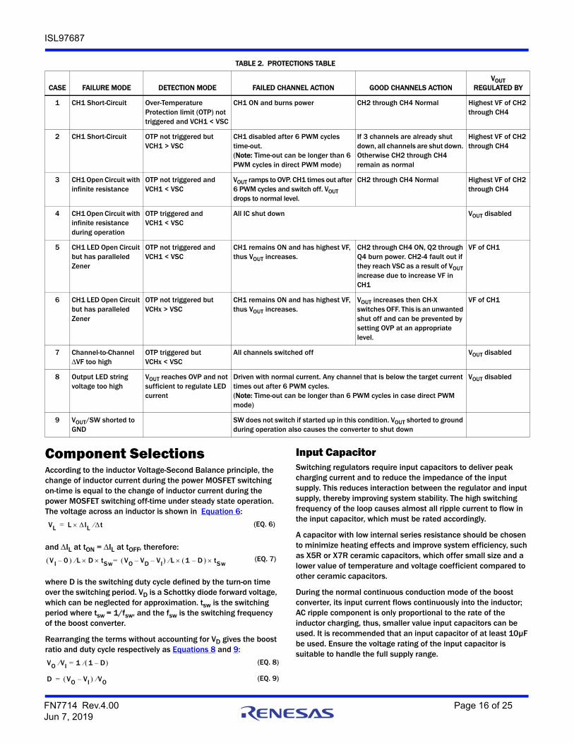
Fault Protection and MonitoringThe ISL97687 features extensive protection functions to cover all perceivable failure conditions. The failure mode of an LED can be either open or short-circuit. The behavior of an open circuit LED can additionally take the form of either infinite or very high resistance or, for some LEDs, a zener diode, which is integrated into the device, in parallel with the now opened LED.
For basic LEDs (which do not have built-in zener diodes) an open circuit LED failure only results in the loss of one LED channel, without affecting other channels. Similarly, a short-circuit condition on a channel that results in that channel being turned off does not affect other channels, unless a similar fault is occurring.
Due to the lag in boost response to any load change at its output, certain transient events (such as significant step changes in LED duty cycle, or a change in LED current caused by CSEL switching) can transiently look like LED fault modes. The ISL97687 uses feedback from the LEDs to determine when it is in a stable operating region and prevents apparent faults during these transient events from allowing any of the LED strings to fault out. See Figure 26 and Table 2 for more details.
fSW5
1010 ROSC
------------------------=(EQ. 4)
ILIMIT0.17RCS------------=
(EQ. 5)
FN7714 Rev.4.00 Page 14 of 25Jun 7, 2019
ISL97687
Short-Circuit Protection (SCP)The short-circuit detection circuit monitors the voltage on each channel and disables faulty channels that are detected to be more than the short-circuit threshold, 8V above the lowest CH pin, following a timeout period.
Open Circuit Protection (OCP)When any of the LEDs become open circuit during the operation, that channel is disabled after a timeout period, and the part continues to drive the other channels. The ISL97687 monitors the current in each channel such that any string which reaches the intended output current is considered “good”. Should the current subsequently fall below the target, the channel is considered an “open circuit”. Furthermore, should the boost output of the ISL97687 reach the OVP limit, all channels which are not “good” are timed out.
Unused CH pins should be grounded, which disables them from start-up. This prevents VOUT having to ramp to OVP at start-up, to determine that they are open.
Undervoltage LockoutIf the input voltage falls below the UVLO level of 2.8V, the device stops switching and resets. Operation restarts, with all digital settings returning to their default states, when the input voltage is back in the normal operating range.
Over-Temperature Protection (OTP)The OTP threshold is set to +150°C. When this is reached, the boost stops switching and the output current sources are switched off and stay off until power or EN is cycled. For the extensive fault protection conditions, see Figure 26 and Table 2.
VIN OVP If VIN exceeds 35V, the part shuts down until power or EN is cycled. At this point, all digital settings are reset to their default states.
ShutdownWhen the EN pin is low the entire chip is shut down to give close to zero shutdown current. The digital interfaces are not active during this time. The EN can be high before VIN.
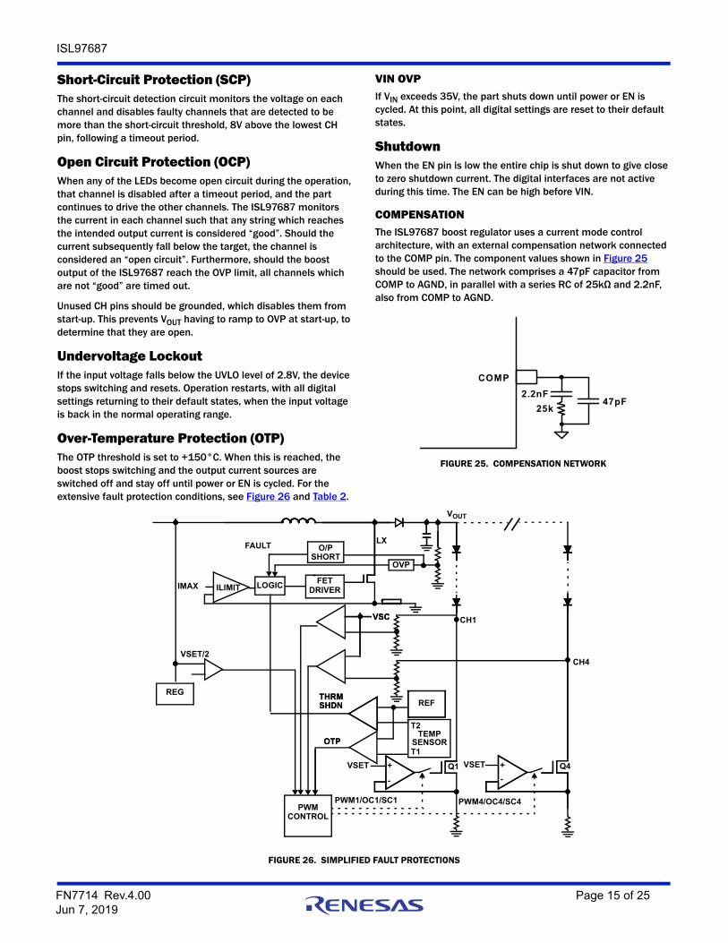
COMPENSATIONThe ISL97687 boost regulator uses a current mode control architecture, with an external compensation network connected to the COMP pin. The component values shown in Figure 25 should be used. The network comprises a 47pF capacitor from COMP to AGND, in parallel with a series RC of 25kΩ and 2.2nF, also from COMP to AGND.
FIGURE 25. COMPENSATION NETWORK
COMP
47pF2.2nF
25k
Q4
VSC
CH4
VSET
PWM1/OC1/SC1
REF
FETDRIVER
LX
IMAX ILIMIT
FAULT
OVP
T2
OTP
THRMSHDN
Q1
VSC CH1
VOUT
PWMCONTROL
VSET
PWM4/OC4/SC4
TEMPSENSOR
LOGIC
T1OTP
THRMSHDN
O/PSHORT
+
-
+
-
REG
VSET/2
FIGURE 26. SIMPLIFIED FAULT PROTECTIONS
FN7714 Rev.4.00 Page 15 of 25Jun 7, 2019
ISL97687
Component SelectionsAccording to the inductor Voltage-Second Balance principle, the change of inductor current during the power MOSFET switching on-time is equal to the change of inductor current during the power MOSFET switching off-time under steady state operation. The voltage across an inductor is shown in Equation 6:
and IL at tON = IL at tOFF, therefore:
where D is the switching duty cycle defined by the turn-on time over the switching period. VD is a Schottky diode forward voltage, which can be neglected for approximation. tsw is the switching period where tsw = 1/fsw, and the fsw is the switching frequency of the boost converter.
Rearranging the terms without accounting for VD gives the boost ratio and duty cycle respectively as Equations 8 and 9:
Input CapacitorSwitching regulators require input capacitors to deliver peak charging current and to reduce the impedance of the input supply. This reduces interaction between the regulator and input supply, thereby improving system stability. The high switching frequency of the loop causes almost all ripple current to flow in the input capacitor, which must be rated accordingly.
A capacitor with low internal series resistance should be chosen to minimize heating effects and improve system efficiency, such as X5R or X7R ceramic capacitors, which offer small size and a lower value of temperature and voltage coefficient compared to other ceramic capacitors.
During the normal continuous conduction mode of the boost converter, its input current flows continuously into the inductor; AC ripple component is only proportional to the rate of the inductor charging, thus, smaller value input capacitors can be used. It is recommended that an input capacitor of at least 10µF be used. Ensure the voltage rating of the input capacitor is suitable to handle the full supply range.
TABLE 2. PROTECTIONS TABLE
CASE FAILURE MODE DETECTION MODE FAILED CHANNEL ACTION GOOD CHANNELS ACTIONVOUT
REGULATED BY
1 CH1 Short-Circuit Over-Temperature Protection limit (OTP) not triggered and VCH1 < VSC
CH1 ON and burns power CH2 through CH4 Normal Highest VF of CH2 through CH4
2 CH1 Short-Circuit OTP not triggered but VCH1 > VSC
CH1 disabled after 6 PWM cycles time-out.(Note: Time-out can be longer than 6 PWM cycles in direct PWM mode)
If 3 channels are already shut down, all channels are shut down. Otherwise CH2 through CH4 remain as normal
Highest VF of CH2 through CH4
3 CH1 Open Circuit with infinite resistance
OTP not triggered and VCH1 < VSC
VOUT ramps to OVP. CH1 times out after 6 PWM cycles and switch off. VOUT drops to normal level.
CH2 through CH4 Normal Highest VF of CH2 through CH4
4 CH1 Open Circuit with infinite resistance during operation
OTP triggered and VCH1 < VSC
All IC shut down VOUT disabled
5 CH1 LED Open Circuit but has paralleled Zener
OTP not triggered and VCH1 < VSC
CH1 remains ON and has highest VF, thus VOUT increases.
CH2 through CH4 ON, Q2 through Q4 burn power. CH2-4 fault out if they reach VSC as a result of VOUT increase due to increase VF in CH1
VF of CH1
6 CH1 LED Open Circuit but has paralleled Zener
OTP not triggered but VCHx > VSC
CH1 remains ON and has highest VF, thus VOUT increases.
VOUT increases then CH-X switches OFF. This is an unwanted shut off and can be prevented by setting OVP at an appropriate level.
VF of CH1
7 Channel-to-Channel VF too high
OTP triggered but VCHx < VSC
All channels switched off VOUT disabled
8 Output LED string voltage too high
VOUT reaches OVP and not sufficient to regulate LED current
Driven with normal current. Any channel that is below the target current times out after 6 PWM cycles.(Note: Time-out can be longer than 6 PWM cycles in case direct PWM mode)
VOUT disabled
9 VOUT/SW shorted to GND
SW does not switch if started up in this condition. VOUT shorted to ground during operation also causes the converter to shut down
VL L IL t= (EQ. 6)
V I 0 L D tSw VO VD VI–– = L 1 D tSw–– (EQ. 7)
VO VI 1 1 D– = (EQ. 8)
D VO VI VO–= (EQ. 9)
FN7714 Rev.4.00 Page 16 of 25Jun 7, 2019
ISL97687
InductorThe selection of the inductor should be based on its maximum current (ISAT) characteristics, power dissipation, EMI susceptibility (shielded vs unshielded), and size. Inductor type and value influence many key parameters, including the inductor ripple current, current limit, efficiency, transient performance, and stability.
The inductor’s maximum current capability must be large enough to handle the peak current at the worst case condition. If an inductor core is chosen with a lower current rating, saturation in the core causes the effective inductor value to fall, leading to an increase in peak to average current level, poor efficiency, and overheating in the core. The series resistance, DCR, within the inductor causes conduction loss and heat dissipation. A shielded inductor is usually more suitable for EMI susceptible applications, such as LED backlighting.
The peak current can be derived from the voltage across the inductor during the off period, as expressed in Equation 10:
The choice of 85% is just an average term for the efficiency approximation. The first term is the average current, which is inversely proportional to the input voltage. The second term is the inductor current change, which is inversely proportional to L and fSW. As a result, for a given switching frequency, minimum input voltage must be used to calculate the input/inductor current as shown in Equation 10. For a given inductor size, the larger the inductance value, the higher the series resistance because of the extra number of turns required, thus, higher conductive losses. The ISL97687 current limit should be less than the inductor saturation current.
Output CapacitorsThe output capacitor acts to smooth the output voltage and supplies load current directly during the conduction phase of the power switch. Output ripple voltage consists of the discharge of the output capacitor during the FET turn-on period and the voltage drop due to load current flowing through the ESR of the output capacitor. The ripple voltage is shown in Equation 11:
where IO represents the output current, CO is the output capacitance, D is the duty ratio as described in Equation 9. ESR is the equivalent series resistance of the output capacitance and fsw is the switching frequency of the converter. Equation 11 shows the importance of using a low ESR output capacitor for minimizing output ripple.
As shown in Equation 11, the output ripple voltage, VCo, can be reduced by increasing the output capacitance, CO or the switching frequency, fSW, or using output capacitors with small ESR. In general, ceramic capacitors are the best choice for output capacitors in small to medium sized LCD backlight applications due to their cost, form factor, and low ESR.
The choice of X7R over Y5V ceramic capacitors is highly recommended because the X7R type capacitor is less sensitive to capacitance change overvoltage. Y5V’s absolute capacitance
can be reduced to 10%~20% of its rated capacitance at the maximum voltage. Because of this, Y5V type ceramic capacitors should be avoided.
A larger output capacitor also eases the driver response during PWM dimming off period due to the longer sample and hold effect of the output drooping. The driver does not need to boost as much on the next on period, which minimizes transient current. The output capacitor also plays an important role for system compensation.
Channel CapacitorIt is recommended to use at least 1nF capacitors from CH pins to VOUT. Larger capacitors reduce LED current ripple at boost frequency, but degrades transient performance at high PWM frequencies. The best value is dependant on PCB layout. Up to 4.7nF is sufficient for most configurations.
Schottky DiodeA high speed rectifier diode is necessary to prevent excessive voltage overshoot, especially in the boost configuration. Low forward voltage and reverse leakage current minimizes losses, making Schottky diodes the preferred choice. Although the Schottky diode turns on only during the boost switch off period, it carries the same peak current as the inductor, therefore, a suitable current rated Schottky diode must be used.
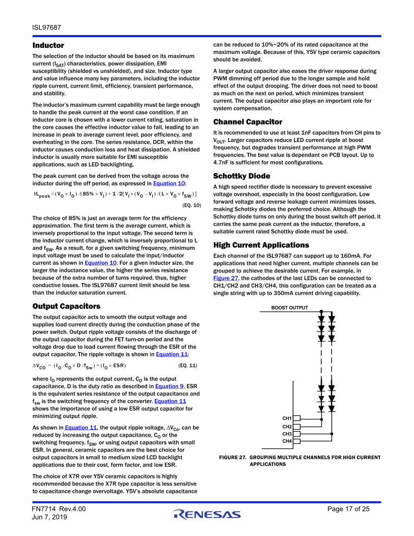
High Current ApplicationsEach channel of the ISL97687 can support up to 160mA. For applications that need higher current, multiple channels can be grouped to achieve the desirable current. For example, in Figure 27, the cathodes of the last LEDs can be connected to CH1/CH2 and CH3/CH4, this configuration can be treated as a single string with up to 350mA current driving capability.
ILpeak VO IO 85% VI 1 2 VI VO VI L VO fSW – +=
(EQ. 10)
VCO I O CO D fSw IO ESR += (EQ. 11)
FIGURE 27. GROUPING MULTIPLE CHANNELS FOR HIGH CURRENT APPLICATIONS
CH1
CH2
CH3
CH4
BOOST OUTPUT
FN7714 Rev.4.00 Page 17 of 25Jun 7, 2019
ISL97687
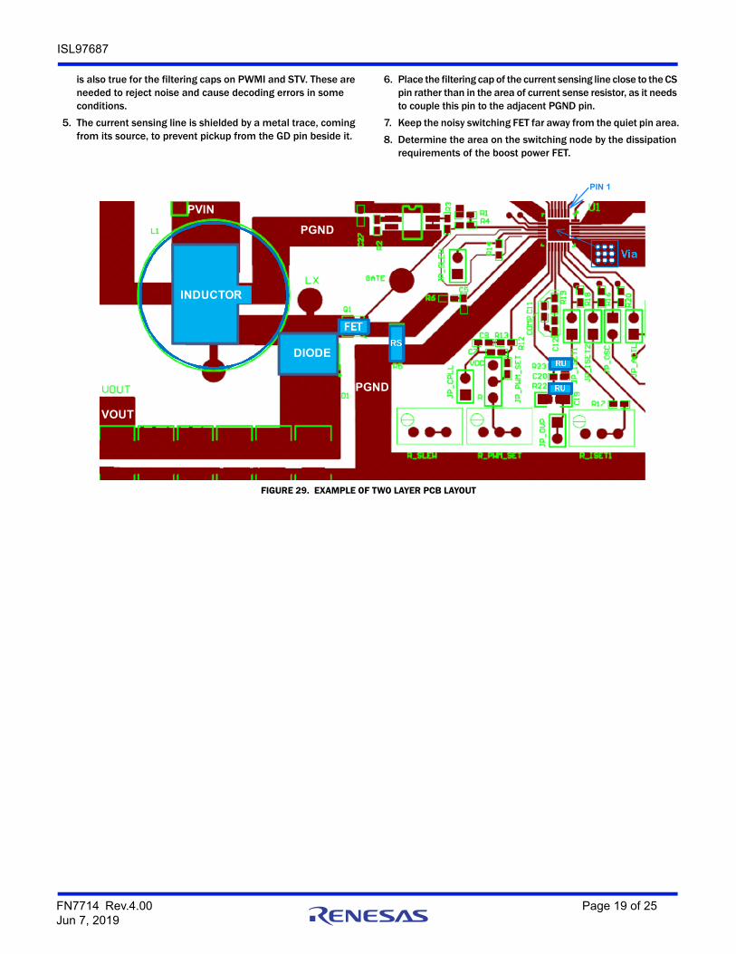
PCB Layout ConsiderationsTwo Layers PCB Layout with TQFN PackageGreat care is needed in designing a PC board for stable ISL97687 operation. As shown in the typical application diagram (Figure 1 on page 1), the separation of PGND and AGND of each ISL97687 is essential, keeping the AGND referenced only local to the chip. This minimizes switching noise injection to the feedback sensing and analog areas, and eliminates DC errors form high current flow in resistive PC board traces. PGND and AGND should be on the top and bottom layers respectively in the two layer PCB. Form a star ground connection by connecting the LED ground return and AGND pins to the thermal pad with 9-12 vias. The ground connection should be into this ground net, on the top plane. The bottom plane then forms a quiet analog ground area, that both shields components on the top plane, and provides easy access to all sensitive components. For example, the ground side of the ISET1/2 resistors can be dropped to the bottom plane, providing a very low impedance path back to the AGND pin, which does not have any circulating high currents to interfere with it. The bottom plane can also be used as a thermal ground, so the AGND area should be sized sufficiently large to dissipate the required power. For multi-layer boards, the AGND plane can be the second layer. This provides easy access to the AGND net, but allows a larger thermal ground and main ground supply to come up through the thermal vias from a lower plane.
This type of layout is particularly important for this type of product, as the ISL97687 has a high power boost, resulting in high current flow in the main loop’s traces. Careful attention should be focussed on the below layout details:
1. Place boost input capacitors, output capacitors, inductor, and Schottky diode together in a nice tight layout. Keeping the grounds of the input, output, ISL97687 and the current sense resistor connected with a low impedance and wide metal is very important to keep these nodes closely coupled.
2. Figure 29 on page 19 shows important traces of current sensor (RS) and OVP resistors (RU, RL). The current sensor track line should be short, so that it remains as close as possible to the Current Sense (CS) pin. Additionally, the CS pin is referenced from the adjacent PGND pin. It is extremely important that this PGND pin is placed with a good reference to the bottom of the sense resistor. In Figure 29 you can see that this ground pin is not connected to the thermal pad, but instead used to effectively sense the voltage at the bottom of the current sense resistor. However, this pin also takes the gate driver current, so it must still have a wide connection and a good connection back from the sense resistor to the star ground. Also, place the RC filter on CS referenced to this PGND pin and close to the chip.
3. If possible, try to maintain central ground node on the board and use the input capacitors to avoid excessive input ripple for high output current supplies. Place the filtering capacitors close by the VIN pin.
4. For optimum load regulation and true VOUT sensing, connect the OVP resistors independently to the top of the output capacitors and away from the higher dv/dt traces. The OVP connection then needs to be as short as possible to the pin. The AGND connection of the lower OVP components is critical
for good regulation. At 70V output, a 100mV change at VOUT translates to a 1.7mV change at OVP, so a small ground error due to high current flow, if referenced to PGND, can be disastrous.
5. The bypass capacitors connected to VDC and VLOGIC need to be as close to the pin as possible, and again should be referenced to AGND. This is also true for the COMP network and the rest of the analog components (on ISEDT1/2, FPWM, etc.).
6. The heat of the chip is mainly dissipated through the exposed thermal pad so maximizing the copper area around it is a good idea. A solid ground is always helpful for the thermal and EMI performance.
7. Mount the inductor and input and output capacitors as tight as possible, to reduce the audible noise and inductive ringing.
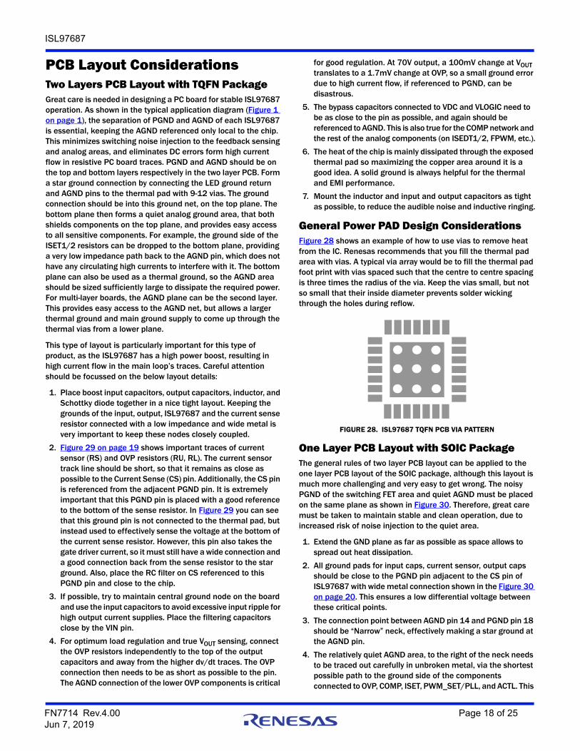
General Power PAD Design ConsiderationsFigure 28 shows an example of how to use vias to remove heat from the IC. Renesas recommends that you fill the thermal pad area with vias. A typical via array would be to fill the thermal pad foot print with vias spaced such that the centre to centre spacing is three times the radius of the via. Keep the vias small, but not so small that their inside diameter prevents solder wicking through the holes during reflow.
One Layer PCB Layout with SOIC PackageThe general rules of two layer PCB layout can be applied to the one layer PCB layout of the SOIC package, although this layout is much more challenging and very easy to get wrong. The noisy PGND of the switching FET area and quiet AGND must be placed on the same plane as shown in Figure 30. Therefore, great care must be taken to maintain stable and clean operation, due to increased risk of noise injection to the quiet area.
1. Extend the GND plane as far as possible as space allows to spread out heat dissipation.
2. All ground pads for input caps, current sensor, output caps should be close to the PGND pin adjacent to the CS pin of ISL97687 with wide metal connection shown in the Figure 30 on page 20. This ensures a low differential voltage between these critical points.
3. The connection point between AGND pin 14 and PGND pin 18 should be “Narrow” neck, effectively making a star ground at the AGND pin.
4. The relatively quiet AGND area, to the right of the neck needs to be traced out carefully in unbroken metal, via the shortest possible path to the ground side of the components connected to OVP, COMP, ISET, PWM_SET/PLL, and ACTL. This
FIGURE 28. ISL97687 TQFN PCB VIA PATTERN
FN7714 Rev.4.00 Page 18 of 25Jun 7, 2019
ISL97687
is also true for the filtering caps on PWMI and STV. These are needed to reject noise and cause decoding errors in some conditions.
5. The current sensing line is shielded by a metal trace, coming from its source, to prevent pickup from the GD pin beside it.
6. Place the filtering cap of the current sensing line close to the CS pin rather than in the area of current sense resistor, as it needs to couple this pin to the adjacent PGND pin.
7. Keep the noisy switching FET far away from the quiet pin area.
8. Determine the area on the switching node by the dissipation requirements of the boost power FET.
FIGURE 29. EXAMPLE OF TWO LAYER PCB LAYOUT
DIODE
INDUCTOR
PGND
PGND
PVIN
VOUT
PIN 1
FN7714 Rev.4.00 Page 19 of 25Jun 7, 2019

ISL97687
FIGURE 30. EXAMPLE OF ONE LAYER PCB LAYOUT
12345671011121314
15
28
27
261716
1918 21
20
CH
3
CH
4
GD
PG
ND
SL
EW
CS
EL
CH
2
CH
1
EN
_V
SY
NC
AC
TL
ISE
T1
CO
MP
VIN
OS
C
VD
CP
GN
D
AG
ND
/SH
UT
VL
OG
ICO
VP
ISE
T2
PG
ND
CS
89
EN
_A
DIM
22
25
24
23
PW
M_
SE
T/P
LL
EN
_PS
PW
MI
ST
V
PVIN
PVOUT
All close to each other with wide metal connection
Narrow connection point of PGND and AGND
Quiet AGND trace
PGND
FN7714 Rev.4.00 Page 20 of 25Jun 7, 2019

ISL97687
Equivalent Circuit Diagrams
VDC
6V
VLOGIC
3V
STV
6V
5200Ω
2MΩ
COMP
VDC
200Ω +
-
OSC
VDC
200Ω
+
-
PWM_SET/PLL
EN_ADIM
EN_PS
EN_VSYNC
LX
VIN
50V
VDC
1000Ω
+
-VLOGIC
2000Ω
EN
50V 2MΩ5V
OVP
CH1~CH4220kΩ
20µA
+
-
50kΩ
CSEL
6V
5200Ω
ISET1
ISET2
VDC
200Ω
CS
GD
20V
VDC
200Ω
40kΩ
VLOGIC
1Ω
1Ω
VIN
SLEW
20V
600Ω
5µA
VDC
VDC
80kΩ
ACTL
50V
600Ω
VDC
PWMI
50V
600Ω
VDC
2MΩ
80V
FN7714 Rev.4.00 Page 21 of 25Jun 7, 2019
ISL97687
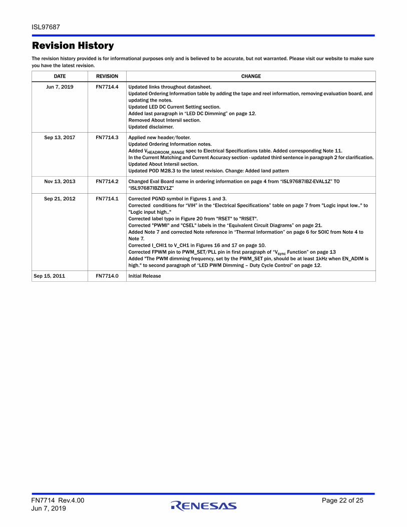
Revision HistoryThe revision history provided is for informational purposes only and is believed to be accurate, but not warranted. Please visit our website to make sure you have the latest revision.
DATE REVISION CHANGE
Jun 7, 2019 FN7714.4 Updated links throughout datasheet.Updated Ordering Information table by adding the tape and reel information, removing evaluation board, and updating the notes.Updated LED DC Current Setting section.Added last paragraph in “LED DC Dimming” on page 12. Removed About Intersil section.Updated disclaimer.
Sep 13, 2017 FN7714.3 Applied new header/footer.Updated Ordering Information notes.Added VHEADROOM_RANGE spec to Electrical Specifications table. Added corresponding Note 11.In the Current Matching and Current Accuracy section - updated third sentence in paragraph 2 for clarification.Updated About Intersil section.Updated POD M28.3 to the latest revision. Change: Added land pattern
Nov 13, 2013 FN7714.2 Changed Eval Board name in ordering information on page 4 from “ISL97687IBZ-EVAL1Z” TO “ISL97687IBZEV1Z”
Sep 21, 2012 FN7714.1 Corrected PGND symbol in Figures 1 and 3.Corrected conditions for “VIH” in the “Electrical Specifications” table on page 7 from "Logic input low.." to "Logic input high.."Corrected label typo in Figure 20 from "RSET" to "RISET".Corrected "PWMI" and "CSEL" labels in the “Equivalent Circuit Diagrams” on page 21.Added Note 7 and corrected Note reference in “Thermal Information” on page 6 for SOIC from Note 4 to Note 7. Corrected I_CHI1 to V_CH1 in Figures 16 and 17 on page 10.Corrected FPWM pin to PWM_SET/PLL pin in first paragraph of “Vsync Function” on page 13Added "The PWM dimming frequency, set by the PWM_SET pin, should be at least 1kHz when EN_ADIM is high." to second paragraph of “LED PWM Dimming – Duty Cycle Control” on page 12.
Sep 15, 2011 FN7714.0 Initial Release
FN7714 Rev.4.00 Page 22 of 25Jun 7, 2019

ISL97687
Package Outline DrawingsL28.5x5B28 LEAD THIN QUAD FLAT NO-LEAD PLASTIC PACKAGERev 1, 10/07
located within the zone indicated. The pin #1 identifier may be
Unless otherwise specified, tolerance : Decimal ± 0.05
Tiebar shown (if present) is a non-functional feature.
The configuration of the pin #1 identifier is optional, but must be
between 0.15mm and 0.30mm from the terminal tip.Dimension b applies to the metallized terminal and is measured
Dimensions in ( ) for Reference Only.
Dimensioning and tolerancing conform to AMSE Y14.5m-1994.
6.
either a mold or mark feature.
3.
5.
4.
2.
Dimensions are in millimeters.1.
NOTES:
BOTTOM VIEW
DETAIL "X"TYPICAL RECOMMENDED LAND PATTERN
TOP VIEW
BOTTOM VIEW
SIDE VIEW
5.00 A
5.0
0
B
INDEX AREAPIN 1
6
(4X) 0.15
28X 0.55 ± 0.05 4
A
28X 0.25 ± 0.05
M0.10 C B
14 8
4X
0.5024X
3.0
6PIN #1 INDEX AREA
3 .25 ± 0 . 10
0 . 75 ± 0.05
BASE PLANE
SEE DETAIL "X"
SEATING PLANE
0.10 CC
0.08 C
0 . 2 REFC
0 . 05 MAX.0 . 00 MIN.
5
( 3. 25)
( 4. 65 TYP )
( 24X 0 . 50)
(28X 0 . 25 )
( 28X 0 . 75)
15
22
21
7
1
28
For the most recent package outline drawing, see L28.5x5B.
FN7714 Rev.4.00 Page 23 of 25Jun 7, 2019
ISL97687
a
INDEXAREA
E
D
N
1 2 3
-B-
0.25(0.010) C AM B S
e
-A-
L
B
M
-C-
A1
A
SEATING PLANE
0.10(0.004)
h x 45o
C
H 0.25(0.010) BM M
(1.50mm)
(9.38mm)
(1.27mm TYP) (0.51mm TYP)
TYPICAL RECOMMENDED LAND PATTERN
M28.3 (JEDEC MS-013-AE ISSUE C)28 Lead Wide Body Small Outline Plastic Package (SOIC)
SYMBOL
INCHES MILLIMETERS
NOTESMIN MAX MIN MAX
A 0.0926 0.1043 2.35 2.65 -
A1 0.0040 0.0118 0.10 0.30 -
B 0.013 0.0200 0.33 0.51 9
C 0.0091 0.0125 0.23 0.32 -
D 0.6969 0.7125 17.70 18.10 3
E 0.2914 0.2992 7.40 7.60 4
e 0.05 BSC 1.27 BSC -
H 0.394 0.419 10.00 10.65 -
h 0.01 0.029 0.25 0.75 5
L 0.016 0.050 0.40 1.27 6
N 28 28 7
0o 8o 0o 8o -
Rev. 1, 1/13
NOTES:
1. Symbols are defined in the “MO Series Symbol List” in Section 2.2 of Publication Number 95.
2. Dimensioning and tolerancing per ANSI Y14.5M-1982.
3. Dimension “D” does not include mold flash, protrusions or gate burrs. Mold flash, protrusion and gate burrs shall not exceed 0.15mm (0.006 inch) per side.
4. Dimension “E” does not include interlead flash or protrusions. Interlead flash and protrusions shall not exceed 0.25mm (0.010 inch) per side.
5. The chamfer on the body is optional. If it is not present, a visual index feature must be located within the crosshatched area.
6. “L” is the length of terminal for soldering to a substrate.
7. “N” is the number of terminal positions.
8. Terminal numbers are shown for reference only.
9. The lead width “B”, as measured 0.36mm (0.014 inch) or greater abovethe seating plane, shall not exceed a maximum value of 0.61mm (0.024inch)
10. Controlling dimension: MILLIMETER. Converted inch dimensions are nonecessarily exact.
For the most recent package outline drawing, see M28.3.
FN7714 Rev.4.00 Page 24 of 25Jun 7, 2019

Corporate HeadquartersTOYOSU FORESIA, 3-2-24 Toyosu,Koto-ku, Tokyo 135-0061, Japanwww.renesas.com
Contact InformationFor further information on a product, technology, the most up-to-date version of a document, or your nearest sales office, please visit:
www.renesas.com/contact/
TrademarksRenesas and the Renesas logo are trademarks of Renesas Electronics Corporation. All trademarks and registered trademarks are the property of their respective owners.