Embed Size (px)
Citation preview
FN6716Rev 0.00
Jun 4, 2008
ISL54105ATMDS Regenerator
DATASHEETKey Features
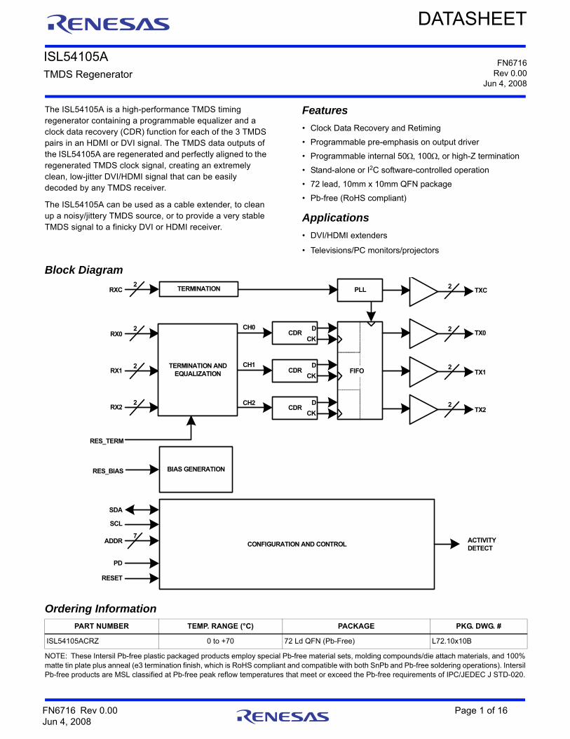
The ISL54105A is a high-performance TMDS timing regenerator containing a programmable equalizer and a clock data recovery (CDR) function for each of the 3 TMDS pairs in an HDMI or DVI signal. The TMDS data outputs of the ISL54105A are regenerated and perfectly aligned to the regenerated TMDS clock signal, creating an extremely clean, low-jitter DVI/HDMI signal that can be easily decoded by any TMDS receiver.
The ISL54105A can be used as a cable extender, to clean up a noisy/jittery TMDS source, or to provide a very stable TMDS signal to a finicky DVI or HDMI receiver.
Features
• Clock Data Recovery and Retiming
• Programmable pre-emphasis on output driver
• Programmable internal 50100, or high-Z termination
• Stand-alone or I2C software-controlled operation
• 72 lead, 10mm x 10mm QFN package
• Pb-free (RoHS compliant)
Applications
• DVI/HDMI extenders
• Televisions/PC monitors/projectors
Block Diagram
2TX1
2TX0
2TXC
2TX2
CONFIGURATION AND CONTROL
RES_BIAS
SCL
PD
RESET
ACTIVITY DETECT
7ADDR
SDA
RX0
2
2
RX1
RX2
CDRCH0
CDRCH1
CDR
2
PLL
RES_TERM
BIAS GENERATION
TERMINATION AND EQUALIZATION
TERMINATIONRXC2
CK
D
CK
D
CK
D
FIFO
CH2
Ordering Information
PART NUMBER TEMP. RANGE (°C) PACKAGE PKG. DWG. #
ISL54105ACRZ 0 to +70 72 Ld QFN (Pb-Free) L72.10x10B
NOTE: These Intersil Pb-free plastic packaged products employ special Pb-free material sets, molding compounds/die attach materials, and 100% matte tin plate plus anneal (e3 termination finish, which is RoHS compliant and compatible with both SnPb and Pb-free soldering operations). Intersil Pb-free products are MSL classified at Pb-free peak reflow temperatures that meet or exceed the Pb-free requirements of IPC/JEDEC J STD-020.
FN6716 Rev 0.00 Page 1 of 16Jun 4, 2008
ISL54105A
Absolute Maximum Ratings Thermal Information
Voltage on VD (referenced to GND). . . . . . . . . . . . . . . . . . . . . . 4.0VVoltage on any Input Pin (referenced to GND) . . . -0.3V to VD+0.3VVoltage on any “5V Tolerant” Input Pin
(referenced to GND). . . . . . . . . . . . . . . . . . . . . . . . -0.3V to +6.0VCurrent into any Output Pin . . . . . . . . . . . . . . . . . . . . . . . . . . ±20mAESD Classification
Human Body Model . . . >4000V, higher voltage testing in progressMachine Model . . . . . . . .>200V, higher voltage testing in progress
Thermal Resistance (Typical, Note 1) JA (°C/W)
QFN Package. . . . . . . . . . . . . . . . . . . . . . . . . . . . . . . . . . 27Maximum Biased Junction Temperature . . . . . . . . . . . . . . . . +125°CStorage Temperature . . . . . . . . . . . . . . . . . . . . . . . . -65°C to +150°CPb-Free Reflow Profile. . . . . . . . . . . . . . . . . . . . . . . . .see link below
http://www.intersil.com/pbfree/Pb-FreeReflow.asp
Recommended Operating ConditionsTemperature . . . . . . . . . . . . . . . . . . . . . . . . . . . . . . . . 0°C to +70°CSupply Voltage. . . . . . . . . . . . . . . . . . . . . . . . . . . . . . . . . . VD = 3.3V
CAUTION: Do not operate at or near the maximum ratings listed for extended periods of time. Exposure to such conditions may adversely impact product reliability andresult in failures not covered by warranty.
NOTE:
1. JA is measured in free air with the component mounted on a high effective thermal conductivity test board with “direct attach” features. See Tech Brief TB379.
Electrical Specifications Specifications apply for VD = 3.3V, pixel rate = 165MHz, TA = +25°C, RES_TERM = 1kRES_BIAS = 3.16kTMDS output load = 50, TMDS output termination voltage VTERM = 3.3V unless otherwise noted.
SYMBOL PARAMETER COMMENTMIN
(Note 2) TYPMAX
(Note 2) UNIT
FULL CHANNEL CHARACTERISTICS
fDATA_MAX Maximum Rx Clock Frequency/Pixel Rate (Note 3) 165 225 MHz
fDATA_MIN Minimum Rx Clock Frequency/Pixel Rate 25 MHz
TMDS RECEIVER CHARACTERISTICS
VSENS Minimum Differential Input Sensitivity 50 150 mVP-P
R50 50 Termination Resistance 45 50 55
R100 100 Termination Resistance 90 97 110
CLKDUTY Rx Clock Duty Cycle 20 80 %
TMDS TRANSMITTER CHARACTERISTICS
jTX_CLOCK Total Jitter on Clock Outputs Independent of incoming jitter 32 ps
jTX_DATA Total Jitter on Data Outputs Independent of incoming jitter 52 ps
SKEWINTRA Intra-Pair (+ to -) Differential Skew ±4 ps
SKEWINTER Inter-Pair (channel-to-channel) Skew Added with respect to incoming inter-pair skew
2 UI
tRISE Rise Time into 50 Load to 3.3V 20% to 80% 80 240 ps
tFALL Fall Time into 50 Load to 3.3V 20% to 80% 80 240 ps
TX VOH Single-Ended High Level Output Voltage VTERM - 10 VTERM + 10 mV
TX VOL Single-Ended Low Level Output Voltage VTERM - 600 VTERM - 400 mV
DIGITAL SCHMITT INPUT CHARACTERISTICS
VIH High Threshold Voltage 2.0 V
VIL High to Low Threshold Voltage 0.8 V
I Input Leakage Current ±10 nA
RPU Internal Pull-Up Resistance SDA and SCL pins 65 k
RPD Internal Pull-Down Resistance AUTO_CH_SEL, CH_SEL_x, RESET, ADDRx, PD pins
60 k
CIN Input Capacitance 5 pF
FN6716 Rev 0.00 Page 2 of 16Jun 4, 2008
ISL54105A
DIGITAL OUTPUT CHARACTERISTICS
VOH Output HIGH Voltage, IO = 8mA 2.4 V
VOL Output LOW Voltage, IO = -8mA 0.4 V
POWER SUPPLY REQUIREMENTS
VD Supply Voltage 3 3.3 3.6 V
ID Supply Current Inputs driven by 165Mpixel/s TMDS signals.Default register settings
357 405 mA
ID Supply Current in Power-down Mode All available inputs driven by 165Mpixel/s TMDS signals.
20 26 mA
AC TIMING CHARACTERISTICS (2-WIRE INTERFACE)
fSCL SCL Clock Frequency 0 400 kHz
tAA SCL LOW to SDA Data Out Valid 200 470 ns
tBUF Time the Bus Must be Free Before a New Transmission Can Start
1.3 µs
tLOW Clock LOW Time 1.3 0.1 µs
tHIGH Clock HIGH Time 0.6 0.2 µs
tSU:STA Start Condition Setup Time 0.6 0.03 µs
tHD:STA Start Condition Hold Time 0.6 0.07 µs
tSU:DAT Data In Setup Time 100 0.03 ns
tHD:DAT Data In Hold Time 0 ns
tSU:STO Stop Condition Setup Time 0.6 µs
tDH Data Output Hold Time 160 ns
NOTE:
2. Parameters with MIN and/or MAX limits are 100% tested at +25°C, unless otherwise specified. Temperature limits established by characterization and are not production tested.
3. Operation up to 165MHz is guaranteed. While many parts will typically operate up to 225MHz, operation above 165MHz is not guaranteed.
Electrical Specifications Specifications apply for VD = 3.3V, pixel rate = 165MHz, TA = +25°C, RES_TERM = 1kRES_BIAS = 3.16kTMDS output load = 50, TMDS output termination voltage VTERM = 3.3V unless otherwise noted.
SYMBOL PARAMETER COMMENTMIN
(Note 2) TYPMAX
(Note 2) UNIT
tSU:STO
tDH
tHIGH
tSU:STAtHD:STA
tHD:DAT
tSU:DATSCL
SDA IN
SDA OUT
tF tLOW
tBUFtAA
tR
FIGURE 1. 2-WIRE INTERFACE TIMING
FN6716 Rev 0.00 Page 3 of 16Jun 4, 2008
ISL54105A
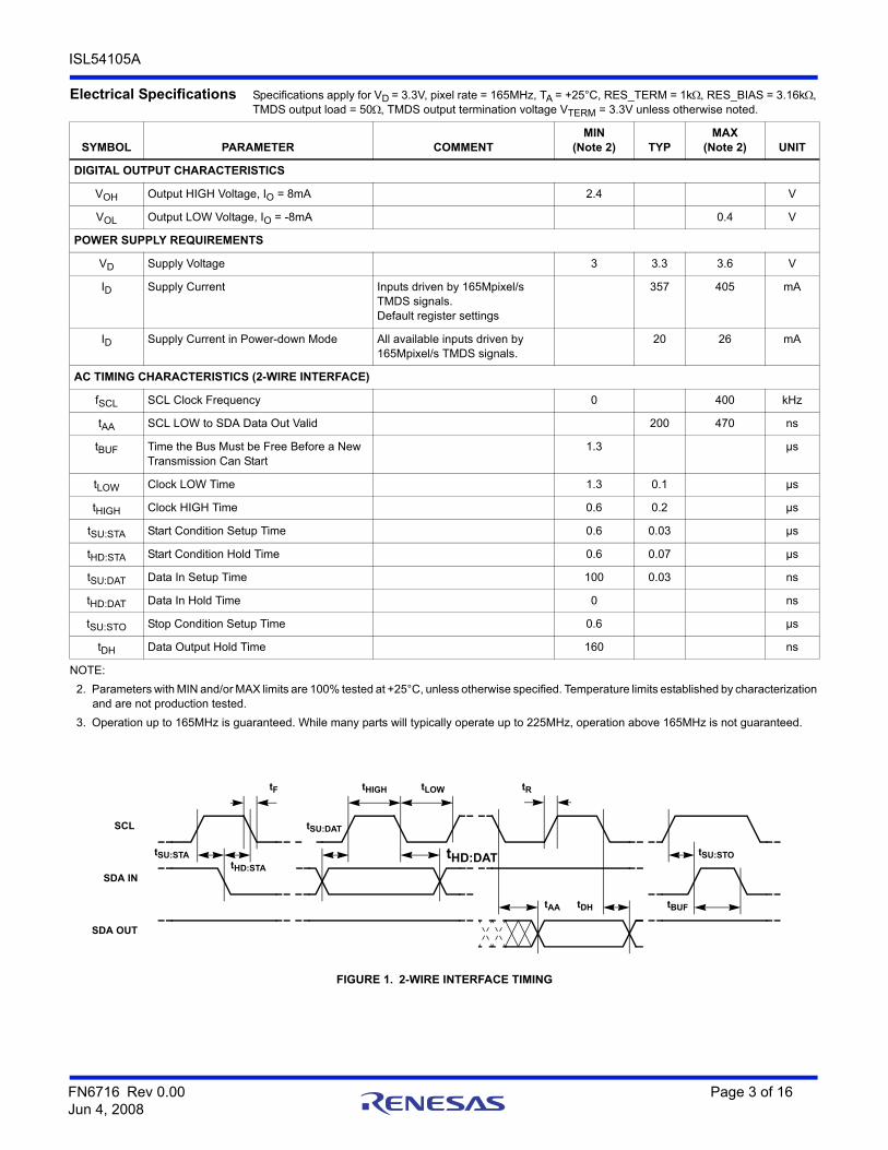
ISL54105A Pin Configuration
NC
NC
NC
AD
DR
2
72 71 70 69 68 67 66 65 64 63 62 61
NC
NC
AD
DR
1
VD
NC
VD
NC
VD
60 59
VD
VD
VD
VD_ESD
VD
VD
TXC+
TXC-
TX2+
TX2-
TX1+
TX1-
TX0+
TX0-
VD
VD_ESD
1
2
3
4
5
6
7
8
9
10
11
12
13
14
54
53
52
51
50
49
48
47
46
45
44
43
42
41
NC
PD
VD
VD
VD
VD
RES_TERM
VD
RES_BIAS
VD
RXC-
RXC+
VD
VD
19 20 21 22 23 24 25 26 27 28 29 30 31 32
AD
DR
3
AD
DR
4
VD
RX
1-
RX
1+
VD
RX
2-
RX
2+
VD
VD
VD
VD
VD
AD
DR
515
16
17
18
RX0-
RX0+
VD
RESET
33 34 35 36
AD
DR
6
NC
VD
NC
VD
TEST
SCL
SDA
40
39
38
37
58 57
NC
AD
DR
0
56 55
AD
NC
FN6716 Rev 0.00 Page 4 of 16Jun 4, 2008
ISL54105A
Pin Descriptions
SYMBOL DESCRIPTION
RX0-, RX0+, RX1-, RX1+, RX2-, RX2+ TMDS Inputs. Incoming TMDS data signals.
RXC-, RXC+ TMDS Inputs. Incoming TMDS clock signals.
TX0-, TX0+, TX1-, TX1+, TX1-, TX1+ TMDS Outputs. TMDS output data for selected channel.
TXC-, TXC+ TMDS Outputs. TMDS output clock for selected channel.
SCL Digital input, 5V tolerant, 500mV hysteresis. Serial data clock for 2-wire interface.Note: Internal 65k pull-up to VD.
SDA Bidirectional Digital I/O, open drain, 5V tolerant. Serial data I/O for 2-wire interface.Note: Internal 65k pull-up to VD.
ADDR[6:0] Digital inputs, 5V tolerant. 7-Bit address for serial interface.Note: Internal 60k pull-down to GND.
AD Digital Output, 3.3V. AD = Activity Detect. Output goes high when an active TMDS clock is detected on RXC.
RES_BIAS Tie to GND through a 3.16k external resistor. Sets up internal bias currents.
RES_TERM Tie to VD through a 1.0k 1% external resistor. During calibration, the termination resistor closest in value to RES_TERM/20 (= 50 is selected.
PD Digital Input, 3.3V. PD = Power-down. Pull high to put the ISL54105A in a minimum power consumption mode. Note: To ensure proper operation, this pin must be held low during power-up. It may be taken high 100ms after the power supplies have settled to 3.3V ±10%. When exiting Power-down, a termination resistor Recalibration cycle must be run to re-trim the termination resistors (see register 0x03[7]).Note: Internal 60k pull-down to GND.
RESET Digital Input, 3.3V. Pull high then low to reset the mux. Tie to GND in final application.Note: Internal 60k pull-down to GND.
TEST Digital Input. Used for production testing only. Tie to GND in final application. This pin has an internal pulldown to GND, so it is also acceptable to leave this pin floating.
VD Power supply. Connect to a 3.3V supply and bypass each pin to GND with 0.1µF.
VD_ESD Power supply for ESD protection diodes. Connect one of these pins (pin 41 or 53) to the 3.3V VD supply rail with a low VF (0.4V or lower) Schottky diode, with the cathode connected to VD_ESD and the anode connected to VD. Bypass each pin to GND with 0.1µF.
THERMAL PAD (GND) Ground return for the entire chip. The thermal pad must have a low impedance connection to GND for the ISL54105A to function at all. The lower electrical impedance, the better the ground, and the better the performance. A low thermal impedance between the thermal pad and the GND plane of the PCB will dissipate the heat from the package more efficiently as well and is recommended.
FN6716 Rev 0.00 Page 5 of 16Jun 4, 2008
ISL54105A
Register Listing
ADDRESS REGISTER (DEFAULT VALUE) BIT(S) FUNCTION NAME DESCRIPTION
0x00 Device ID (read only) 3:0 Device Revision 1 = initial silicon, 2 = second revision, etc.
7:4 Device ID 3 = ISL54105A
0x01 Channel Activity Detect (read only) 1:0 Reserved Reserved
2 Activity Detect 0: TMDS clock not present on RXC1: TMDS clock detected on RXC
0x02 Channel Selection (0x0C) 3:0 Reserved This nibble should always be set to 0xC.
4 Reset Full chip reset. Write a 1 to reset. Will set itself to 0 when reset is complete.
5 Power-down 0: Normal Operation1: Puts the chip in a minimal power consumption mode, turning off all TMDS outputs and open-circuiting all TMDS inputs. This bit is OR'ed with the Power-down input pin. If either is set, the chip will enter power-down. Serial I/O stays operational in PD mode. Note: When exiting Power-down, a termination resistor Recalibration cycle must be run to re-trim the termination resistors (see register 0x03[7]).
0x03 Input Control (0x12)Recommended default: 0x63
0 Reserved Set to 1. Default value of 0 is OK, set to 1 to slightly reduce power consumption.
1 Reserved Set to 1.
2 Tri-state Clock Inputs
0: Clock inputs are terminated into 50/100.1: Clock inputs are tri-stated (to allow chip to operate in parallel with another TMDS receiver with fixed 50termination)
3 Tri-state Data Inputs 0: Data inputs are terminated into 50/100.1: Data inputs are tri-stated (to allow chip to operate in parallel with another TMDS receiver with fixed 50termination)
4 Activity Detect Mode 0: AC Activity. Activity detection is based on the presence of AC activity on TMDS clock inputs. This setting (along with a hysteresis of 20mV enabled) provides reliable activity detection. (recommended setting)1: Common Mode Voltage. If the common mode voltage is above ~3.05V, the input is considered in active. This method has been found to be unreliable with small signal swings and should not be used. This setting is the silicon default but should be changed in software for more reliable activity detection.
5 Clock Rx Hysteresis Enables hysteresis for the clock inputs to prevent false clock detection when both inputs are high. Data inputs do not get hysteresis.0: TMDS input hysteresis disabled1: TMDS input hysteresis enabled. Eliminates false activity detects on unconnected channels. (recommended setting)
6 Clock Rx Hysteresis Magnitude
Controls the amount of hysteresis in the clock inputs.0: 10mV1: 20mV (recommended setting)
7 Recalibrate 0: Normal Operation1: Recalibrates termination resistance. To recalibrate, take this bit high, wait at least 1ms, then take this bit low. Calibration is automatically done after power-on, but performing a recalibration after the supply voltage and temperature have stabilized may result in termination resistances closer to the desired 50.
FN6716 Rev 0.00 Page 6 of 16Jun 4, 2008
ISL54105A
0x04 Termination Control (0x00) 1:0 Reserved Set to 00.
2 Data Termination 0: TMDS Data inputs terminated into 50 (normal operation)1: TMDS Data inputs terminated into 100 (for paralleled inputs)
5:3 Reserved Set to 000.
6 Clk Termination 0: TMDS Clock inputs terminated into 50 (normal operation)1: TMDS Clock inputs terminated into 100 (for paralleled inputs)
7 Reserved Set to 0.
0x05 Output Options (0x00) 0 Tri-state Clock Outputs
0: Normal Operation1: Clock outputs tri-stated (allows another chip to drive the output clock pins)
1 Tri-state Data Outputs
0: Normal Operation1: Data outputs tri-stated (allows another chip to drive the output data pins)
2 Invert Output Polarity
0: Normal Operation1: The polarity of the TMDS data outputs is inverted (+ becomes -, - becomes +). TMDS clock unchanged.
3 Reverse Output Order
0: Normal Operation1: CH0 data is output on CH2 and CH2 data is output on CH0. No change to CH1.
0x06 Data Output Drive (0x00) 3:0 Transmit Current Transmit Drive Current for data signals, adjustable in 0.125mA steps. Clock current is fixed at 10mA.0x0: 10mA0x8: 11mA0xF: 11.875mA
7:4 Transmit Pre-emphasis
Drive boost (in 0.125mA steps) added during first half of each bit period for data signals. Clock signals do not have pre-emphasis.0x0: 0mA0x8: 1mA0xF: 1.875mA
0x07 Reserved (0xCC) 7:0 Reserved Default value of 0xCC is OK, can also be set to 0x00.
0x08 Equalization (0xCC) 3:0 Equalizer Gain Boost (dB) = 1dB + <gain value> * 0.8dB
0x0: 1dB boost at 800MHz0xC: 10.6dB boost at 800MHz (default)0xF: 13dB boost at 800MHz
7:4 Reserved Default value of 0xC is OK, can also be set to 0x0.
0x09 Test Pattern Generator (0x00) 1:0 Generator Mode When a 25MHz to 165MHz clock is applied to the clock input, this function will output a PRBS7 pattern on the TX pins.0: Normal operation (test patterns disabled)1: PRBS7 pattern 2: Low frequency toggle (0000011111…)3: High frequency toggle (1010101010…)Note: When switching from the high frequency toggle pattern to the low frequency toggle pattern, you must first select normal operation.
2 Enable PRBS7 Error Counter
Enables PRBS7 error counter in registers 0x0A to 0x0C.0: Disable PRBS7 Error Counter1: Enable PRBS7 Error Counter
Register Listing (Continued)
ADDRESS REGISTER (DEFAULT VALUE) BIT(S) FUNCTION NAME DESCRIPTION
FN6716 Rev 0.00 Page 7 of 16Jun 4, 2008

ISL54105A
0x0A PRBS7 Error Counter Link 0 (read only) 7:0 PRBS7 Error Counter Link 0
PRBS7 Error Counter of Link 0. Saturates at 0xFF. Reading this register clears this register at end of read
0x0B PRBS7 Error Counter Link 1 (read only) 7:0 PRBS7 Error Counter Link 1
PRBS7 Error Counter of Link 1. Saturates at 0xFF. Reading this register clears this register at end of read
0x0C PRBS7 Error Counter Link 2 (read only) 7:0 PRBS7 Error Counter Link 2
PRBS7 Error Counter of Link 2. Saturates at 0xFF. Reading this register clears this register at end of read
0x10 PLL Bandwidth (0x10)Recommended default: 0x12
1:0 PLL Bandwidth Selects between 4 PLL bandwidth settings0: 4MHz (silicon default)1: 2MHz2: 1MHz (recommended default)3: 500kHz1MHz provides slightly better performance with high jitter/high noise signals.
7:2 Reserved Keep set to 000100 binary.
Register Listing (Continued)
ADDRESS REGISTER (DEFAULT VALUE) BIT(S) FUNCTION NAME DESCRIPTION
FN6716 Rev 0.00 Page 8 of 16Jun 4, 2008

ISL54105A
Application InformationThe ISL54105A is a TMDS regenerator, locking to the incoming DVI or HDMI signal with triple Clock Data Recovery units (CDRs) and a Phase Locked Loop (PLL). The PLL generates a low jitter pixel clock from the incoming TMDS clock. The TMDS data signals are equalized, sliced by the CDR, re-aligned to the PLL clock, and sent out the TMDS outputs.
Activity DetectionThe TMDS input is considered active using one of two methods. The original default activity detect method (register 0x03b4 = 1) is to measure the common mode of the TMDS clock input for each channel. If the common mode is 3.3V, it indicates that there is nothing connected to that input, or that whatever is connected is turned off (inactive). This has been found to be relatively unreliable, particularly with weak signals.
The preferred method of activity detection is looking for an active AC signal on the TMDS clock input for that channel (register 0x03b4 = 1). This is more robust, however disconnected inputs will cause both inputs to the differential receiver to be the same level - 3.3V. If the offset error of the differential TMDS receiver is very small, the receiver can not resolve a 1 or a 0 and will randomly switch between states, which may be detected as an active clock. Register 0x03 bits 5 and 6 allow a 10mV or 20mV offset to be added to the input stage of the clock inputs, eliminating this problem. This offset will slightly reduce the sensitivity of TMDS receiver for the clock lines, but since the clock signals are much lower frequency than the data, they will not be nearly as attenuated, so this is not a problem in practice.
Again, using the AC activity detection method (register 0x03b4 = 0) is recommended.
Rx EqualizationRegister 0x08 bits 3:0 control the amount of equalization applied to the TMDS inputs, providing 4 bits of control. The equalization range available is from a minimum of 1dB boost to a maximum of 13dB at 800MHz, in 0.8dB increments. Ideally, the equalization is adjusted in the final application to provide optimal performance with the specific DVI/HDMI transmitter and cable used. In general, the amount of equalization required is proportional to the cable length. If the equalization must be fixed (can not be adjusted in the final application), an equalization setting of 0xA works well with short cables as well as medium to longer cables.
Tx Pre-emphasisThe transmit pre-emphasis function sinks additional current during the first bit after every transition, increasing the slew rate for a given capacitance, and helping to maintain the slew rate when using longer/higher capacitance cables. Pre-emphasis is controlled by register 0x06 bits 7:4, and ranges from a minimum of 0mA (no pre-emphasis) to 1.875mA (max pre-emphasis).
PLL BandwidthThe 2-bit PLL Bandwidth register controls the loop bandwidth of the PLL used to recover the incoming clock signal. The default 4MHz setting works well in most applications, however a lower bandwidth of 1MHz has proven to work just as well with good TMDS sources and slightly better with marginal sources.
Power-downThe chip can be placed in a Power-down mode when not in use to conserve power. Setting the Power-down bit (register 0x02 bit 5) to a 1 or pulling the PD input pin high places the chip in a minimal power consumption mode, turning off all TMDS outputs and disconnecting all TMDS inputs. Serial I/O stays operational in PD mode. Note that the PD pin must be low during power-on in order to initialize the I2C interface.
Note: When exiting Power-down, a termination resistor Recalibration cycle must be run to re-trim the termination resistors (see register 0x03[7]).
Typical PerformanceSetup A (Figure 2) was used to capture the TMDS eye diagrams shown in Figure 3 and Figure 4:
The 162.5Mpixel/s (UXGA 60Hz) DVI output of the Chroma 2326 was terminated into a TPA2 Plug adapter and measured with a LeCroy differential probe and 6MHz SDA using the LeCroy’s software clock recovery. As Figure 3 shows, the amplitude of the TMDS signal is slightly low, but the eye is otherwise acceptable.
CHROMA 2326 VIDEO PATTERN GENERATOR @
UXGA 60Hz
DELL 2000FP UXGA MONITOR
15m DUAL-LINK DVI CABLE
FIGURE 2. TEST SETUP A
FIGURE 3 FIGURE 4
FIGURE 3. EYE DIAGRAM AT OUTPUT OF CHROMA GENERATOR
FN6716 Rev 0.00 Page 9 of 16Jun 4, 2008
ISL54105A
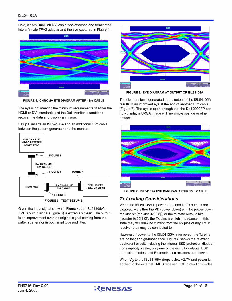
Next, a 15m DualLink DVI cable was attached and terminated into a female TPA2 adapter and the eye captured in Figure 4.
The eye is not meeting the minimum requirements of either the HDMI or DVI standards and the Dell Monitor is unable to recover the data and display an image.
Setup B inserts an ISL54105A and an additional 15m cable between the pattern generator and the monitor:
Given the input signal shown in Figure 4, the ISL54105A’s TMDS output signal (Figure 6) is extremely clean. The output is an improvement over the original signal coming from the pattern generator in both amplitude and jitter.
The cleaner signal generated at the output of the ISL54105A results in an improved eye at the end of another 15m cable (Figure 7). The eye is open enough that the Dell 2000FP can now display a UXGA image with no visible sparkle or other artifacts.
Tx Loading ConsiderationsWhen the ISL54105A is powered-up and its Tx outputs are disabled, via either the PD (power down) pin, the power-down register bit (register 0x02[5]), or the tri-state outputs bits (register 0x05[1:0]), the Tx pins are high impedance. In this state they will draw no current from the Rx pins of any TMDS receiver they may be connected to.
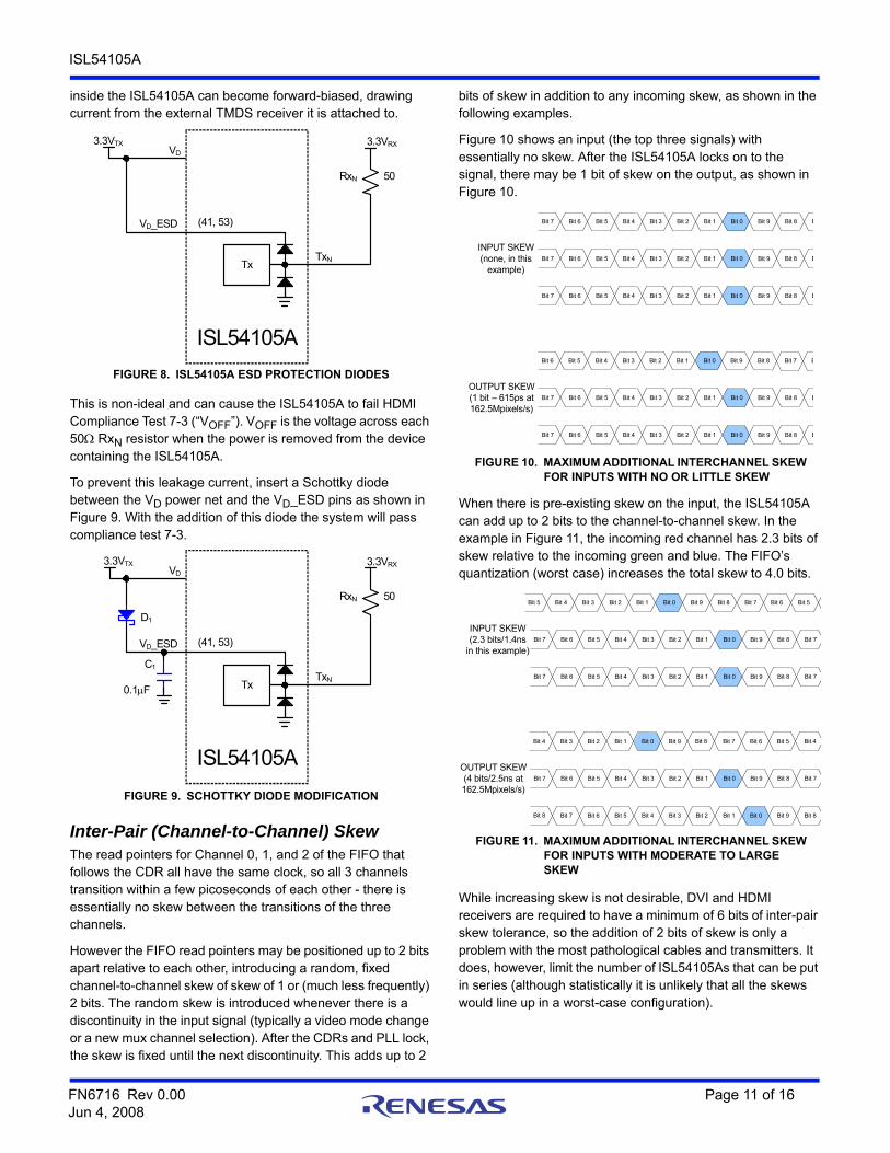
However, if power to the ISL54105A is removed, the Tx pins are no longer high-impedance. Figure 8 shows the relevant equivalent circuit, including the internal ESD protection diodes. For simplicity’s sake, only one of the eight Tx outputs, ESD protection diodes, and Rx termination resistors are shown.
When VD to the ISL54105A drops below ~2.7V and power is applied to the external TMDS receiver, ESD protection diodes
FIGURE 4. CHROMA EYE DIAGRAM AFTER 15m CABLE
CHROMA 2326 VIDEO PATTERN
GENERATOR
15m DUAL-LINK DVI CABLE
DELL 2000FP UXGA MONITOR
ISL54105A 15m DUAL-LINK DVI CABLE
FIGURE 5. TEST SETUP B
FIGURE 6
FIGURE 3
FIGURE 4 FIGURE 7
FIGURE 6. EYE DIAGRAM AT OUTPUT OF ISL54105A
FIGURE 7. ISL54105A EYE DIAGRAM AFTER 15m CABLE
FN6716 Rev 0.00 Page 10 of 16Jun 4, 2008
ISL54105A
inside the ISL54105A can become forward-biased, drawing current from the external TMDS receiver it is attached to.
This is non-ideal and can cause the ISL54105A to fail HDMI Compliance Test 7-3 (“VOFF”). VOFF is the voltage across each 50 RxN resistor when the power is removed from the device containing the ISL54105A.
To prevent this leakage current, insert a Schottky diode between the VD power net and the VD_ESD pins as shown in Figure 9. With the addition of this diode the system will pass compliance test 7-3.
Inter-Pair (Channel-to-Channel) SkewThe read pointers for Channel 0, 1, and 2 of the FIFO that follows the CDR all have the same clock, so all 3 channels transition within a few picoseconds of each other - there is essentially no skew between the transitions of the three channels.
However the FIFO read pointers may be positioned up to 2 bits apart relative to each other, introducing a random, fixed channel-to-channel skew of skew of 1 or (much less frequently) 2 bits. The random skew is introduced whenever there is a discontinuity in the input signal (typically a video mode change or a new mux channel selection). After the CDRs and PLL lock, the skew is fixed until the next discontinuity. This adds up to 2
bits of skew in addition to any incoming skew, as shown in the following examples.
Figure 10 shows an input (the top three signals) with essentially no skew. After the ISL54105A locks on to the signal, there may be 1 bit of skew on the output, as shown in Figure 10.
When there is pre-existing skew on the input, the ISL54105A can add up to 2 bits to the channel-to-channel skew. In the example in Figure 11, the incoming red channel has 2.3 bits of skew relative to the incoming green and blue. The FIFO’s quantization (worst case) increases the total skew to 4.0 bits.
While increasing skew is not desirable, DVI and HDMI receivers are required to have a minimum of 6 bits of inter-pair skew tolerance, so the addition of 2 bits of skew is only a problem with the most pathological cables and transmitters. It does, however, limit the number of ISL54105As that can be put in series (although statistically it is unlikely that all the skews would line up in a worst-case configuration).
FIGURE 8. ISL54105A ESD PROTECTION DIODES
ISL54105A
VD
VD_ESD (41, 53)
3.3VTX
TxNTx
3.3VRX
50RxN
FIGURE 9. SCHOTTKY DIODE MODIFICATION
ISL54105A
VD
VD_ESD (41, 53)
3.3VTX
TxNTx
3.3VRX
50RxN
D1
C1
0.1F
FIGURE 10. MAXIMUM ADDITIONAL INTERCHANNEL SKEW FOR INPUTS WITH NO OR LITTLE SKEW
Bit 4Bit 5Bit 6Bit 7 Bit 0Bit 1Bit 2Bit 3 BBit 8Bit 9
Bit 4Bit 5Bit 6Bit 7 Bit 0Bit 1Bit 2Bit 3 BBit 8Bit 9
Bit 4Bit 5Bit 6Bit 7 Bit 0Bit 1Bit 2Bit 3 BBit 8Bit 9
Bit 4Bit 5Bit 6 Bit 0Bit 1Bit 2Bit 3 BBit 7Bit 8Bit 9
Bit 4Bit 5Bit 6Bit 7 Bit 0Bit 1Bit 2Bit 3 BBit 8Bit 9
Bit 4Bit 5Bit 6Bit 7 Bit 0Bit 1Bit 2Bit 3 BBit 8Bit 9
INPUT SKEW(none, in this
example)
OUTPUT SKEW(1 bit – 615ps at 162.5Mpixels/s)
FIGURE 11. MAXIMUM ADDITIONAL INTERCHANNEL SKEW FOR INPUTS WITH MODERATE TO LARGE SKEW
Bit 4Bit 5 Bit 0Bit 1Bit 2Bit 3 Bit 7Bit 8Bit 9
Bit 4Bit 5Bit 6Bit 7 Bit 0Bit 1Bit 2Bit 3 Bit 7Bit 8Bit 9
Bit 4Bit 5Bit 6Bit 7 Bit 0Bit 1Bit 2Bit 3 Bit 7Bit 8Bit 9
Bit 4 Bit 0Bit 1Bit 2Bit 3 Bit 6Bit 7
Bit 8
Bit 9
Bit 4Bit 5Bit 6Bit 7 Bit 0Bit 1Bit 2Bit 3 Bit 7Bit 8Bit 9
Bit 4Bit 5Bit 6Bit 7 Bit 0Bit 1Bit 2Bit 3 Bit 8Bit 9
INPUT SKEW(2.3 bits/1.4ns
in this example)
OUTPUT SKEW(4 bits/2.5ns at 162.5Mpixels/s)
Bit 5Bit 6
Bit 4Bit 5Bit 8
FN6716 Rev 0.00 Page 11 of 16Jun 4, 2008
ISL54105A
PCB Layout RecommendationsBecause of the high speed of the TMDS signals, careful PCB layout is critical to maximize performance. The following guidelines should be adhered to as closely as possible:
• All TMDS pair traces should have a characteristic impedance of 50 with respect to the power/ground planes and 100 with respect to each other. Failure to meet this requirement will increase reflections, shrinking the available eye.
• Avoid vias for all 3 high speed TMDS pairs. Vias add inductance which causes a discontinuity in the characteristic impedance of the trace. Keep all the traces on the top (or the bottom) of the PCB. The TMDS clock can have vias if necessary, since it is lower speed and less critical. If you must use a via, ensure the vias are symmetrical (put identical vias in both lines of the differential pair).
• For each TMDS channel, the trace lengths of the 3 TMDS pairs (0, 1 and 2) should ideally be the same to reduce inter channel skew introduced by the board.
• The trace length of the clock pair is not critical at all. Since the clock is only used as a frequency reference, its phase/delay is inconsequential. In addition, since the TMDS clock frequency is 1/10th the pixel rate, the clock signal itself is much more noise-immune. So liberties (such as vias and circuitous paths) can be taken when routing the clock lines.
• Minimize capacitance on all TMDS lines. The lower the capacitance, the sharper the rise and fall times.
• Maintain a constant, solid ground (or power) plane under the 3 high speed TMDS signals. Do not route the signals over gaps in the ground plane or over other traces.
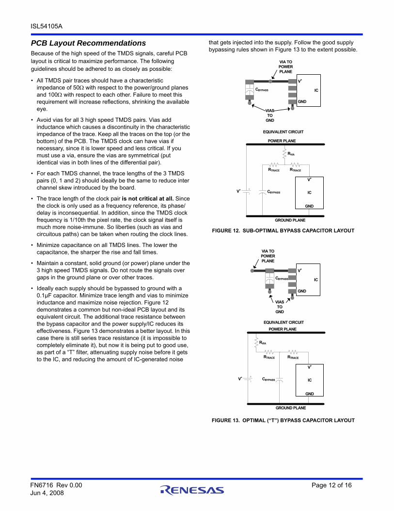
• Ideally each supply should be bypassed to ground with a 0.1µF capacitor. Minimize trace length and vias to minimize inductance and maximize noise rejection. Figure 12 demonstrates a common but non-ideal PCB layout and its equivalent circuit. The additional trace resistance between the bypass capacitor and the power supply/IC reduces its effectiveness. Figure 13 demonstrates a better layout. In this case there is still series trace resistance (it is impossible to completely eliminate it), but now it is being put to good use, as part of a “T” filter, attenuating supply noise before it gets to the IC, and reducing the amount of IC-generated noise
that gets injected into the supply. Follow the good supply bypassing rules shown in Figure 13 to the extent possible.
FIGURE 12. SUB-OPTIMAL BYPASS CAPACITOR LAYOUT
CBYPASS
RTRACE
V+
RTRACE
IC
V+
GND
GROUND PLANE
POWER PLANE
CBYPASS IC
V+
GND
VIAS TO
GND
VIA TO POWER PLANE
EQUIVALENT CIRCUIT
RVIA
FIGURE 13. OPTIMAL (“T”) BYPASS CAPACITOR LAYOUT
CBYPASS
RTRACE
V+
RTRACE
IC
V+
GND
GROUND PLANE
CBYPASS IC
V+
GND
VIAS TO
GND
VIA TO POWER PLANE
EQUIVALENT CIRCUIT
POWER PLANE
RVIA
FN6716 Rev 0.00 Page 12 of 16Jun 4, 2008
ISL54105A
ISL54105A Serial Communication
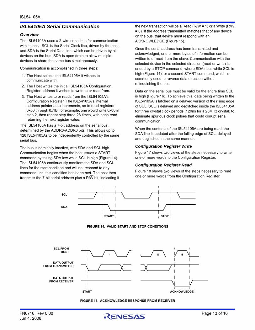
Overview
The ISL54105A uses a 2-wire serial bus for communication with its host. SCL is the Serial Clock line, driven by the host and SDA is the Serial Data line, which can be driven by all devices on the bus. SDA is open drain to allow multiple devices to share the same bus simultaneously.
Communication is accomplished in three steps:
1. The Host selects the ISL54105A it wishes to communicate with.
2. The Host writes the initial ISL54105A Configuration Register address it wishes to write to or read from.
3. The Host writes to or reads from the ISL54105A’s Configuration Register. The ISL54105A’s internal address pointer auto increments, so to read registers 0x00 through 0x1B, for example, one would write 0x00 in step 2, then repeat step three 28 times, with each read returning the next register value.
The ISL54105A has a 7-bit address on the serial bus, determined by the ADDR0-ADDR6 bits. This allows up to 128 ISL54105As to be independently controlled by the same serial bus.
The bus is nominally inactive, with SDA and SCL high. Communication begins when the host issues a START command by taking SDA low while SCL is high (Figure 14). The ISL54105A continuously monitors the SDA and SCL lines for the start condition and will not respond to any command until this condition has been met. The host then transmits the 7-bit serial address plus a R/W bit, indicating if
the next transaction will be a Read (R/W = 1) or a Write (R/W = 0). If the address transmitted matches that of any device on the bus, that device must respond with an ACKNOWLEDGE (Figure 15).
Once the serial address has been transmitted and acknowledged, one or more bytes of information can be written to or read from the slave. Communication with the selected device in the selected direction (read or write) is ended by a STOP command, where SDA rises while SCL is high (Figure 14), or a second START command, which is commonly used to reverse data direction without relinquishing the bus.
Data on the serial bus must be valid for the entire time SCL is high (Figure 16). To achieve this, data being written to the ISL54105A is latched on a delayed version of the rising edge of SCL. SCL is delayed and deglitched inside the ISL54105A for three crystal clock periods (120ns for a 25MHz crystal) to eliminate spurious clock pulses that could disrupt serial communication.
When the contents of the ISL54105A are being read, the SDA line is updated after the falling edge of SCL, delayed and deglitched in the same manner.
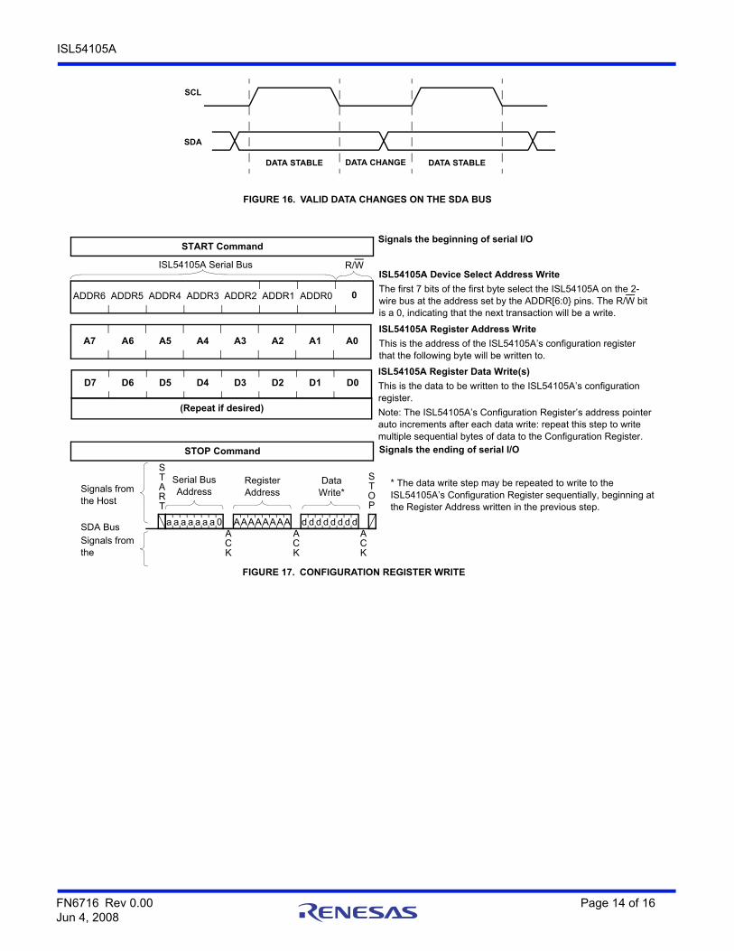
Configuration Register Write
Figure 17 shows two views of the steps necessary to write one or more words to the Configuration Register.
Configuration Register Read
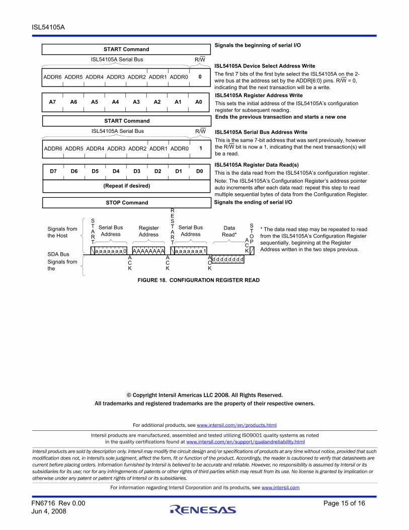
Figure 18 shows two views of the steps necessary to read one or more words from the Configuration Register.
SCL
SDA
START STOP
FIGURE 14. VALID START AND STOP CONDITIONS
SCL FROMHOST
DATA OUTPUTFROM TRANSMITTER
DATA OUTPUTFROM RECEIVER
81 9
START ACKNOWLEDGE
FIGURE 15. ACKNOWLEDGE RESPONSE FROM RECEIVER
FN6716 Rev 0.00 Page 13 of 16Jun 4, 2008
ISL54105A
SCL
SDA
DATA STABLE DATA CHANGE DATA STABLE
FIGURE 16. VALID DATA CHANGES ON THE SDA BUS
D7 D6 D5 D2D4 D3 D1 D0
A0A7 A2A4 A3 A1
ISL54105A Register Data Write(s)
This is the data to be written to the ISL54105A’s configuration register.
Note: The ISL54105A’s Configuration Register’s address pointer auto increments after each data write: repeat this step to write multiple sequential bytes of data to the Configuration Register.
A6 A5
0
R/W
ISL54105A Register Address Write
This is the address of the ISL54105A’s configuration register that the following byte will be written to.
ISL54105A Serial Bus
FIGURE 17. CONFIGURATION REGISTER WRITE
START Command
STOP Command
(Repeat if desired)
Signals the beginning of serial I/O
Signals the ending of serial I/O
START
STOP
Data Write*
Register Address
Serial Bus Address
ACK
AAAAAAAAACK
d d d d d d d dACK
a a a a a a a 0
* The data write step may be repeated to write to the ISL54105A’s Configuration Register sequentially, beginning at the Register Address written in the previous step.
SDA BusSignals from the
Signals from the Host
ISL54105A Device Select Address Write
The first 7 bits of the first byte select the ISL54105A on the 2-wire bus at the address set by the ADDR[6:0} pins. The R/W bit is a 0, indicating that the next transaction will be a write.
ADDR1 ADDR0ADDR3 ADDR2ADDR5 ADDR4ADDR6
FN6716 Rev 0.00 Page 14 of 16Jun 4, 2008
ISL54105A
Intersil products are manufactured, assembled and tested utilizing ISO9001 quality systems as notedin the quality certifications found at www.intersil.com/en/support/qualandreliability.html
Intersil products are sold by description only. Intersil may modify the circuit design and/or specifications of products at any time without notice, provided that such modification does not, in Intersil's sole judgment, affect the form, fit or function of the product. Accordingly, the reader is cautioned to verify that datasheets are current before placing orders. Information furnished by Intersil is believed to be accurate and reliable. However, no responsibility is assumed by Intersil or its subsidiaries for its use; nor for any infringements of patents or other rights of third parties which may result from its use. No license is granted by implication or otherwise under any patent or patent rights of Intersil or its subsidiaries.
For information regarding Intersil Corporation and its products, see www.intersil.com
For additional products, see www.intersil.com/en/products.html
© Copyright Intersil Americas LLC 2008. All Rights Reserved.All trademarks and registered trademarks are the property of their respective owners.
FIGURE 18. CONFIGURATION REGISTER READ
A0A7 A2A4 A3 A1A6 A5
R/W
ISL54105A Register Address Write
This sets the initial address of the ISL54105A’s configuration register for subsequent reading.
ISL54105A Serial Bus
START CommandSignals the beginning of serial I/O
ISL54105A Serial Bus Address Write
This is the same 7-bit address that was sent previously, however the R/W bit is now a 1, indicating that the next transaction(s) will be a read.
D7 D6 D5 D2D4 D3 D1 D0ISL54105A Register Data Read(s)
This is the data read from the ISL54105A’s configuration register.
Note: The ISL54105A’s Configuration Register’s address pointer auto increments after each data read: repeat this step to read multiple sequential bytes of data from the Configuration Register.
R/WISL54105A Serial Bus
START Command
STOP Command
(Repeat if desired)
Ends the previous transaction and starts a new one
Signals the ending of serial I/O
START
STOP
Data Read*
SDA Bus
Signals from the
Signals from the Host
Register Address
Serial Bus Address
ACK
AAAAAAAA
ACK
d d d d d d d dACK
a a a a a a a 0
* The data read step may be repeated to read from the ISL54105A’s Configuration Register sequentially, beginning at the Register Address written in the two steps previous.
RESTART
Serial Bus Address
ACK
a a a a a a a 1
ISL54105A Device Select Address Write
The first 7 bits of the first byte select the ISL54105A on the 2-wire bus at the address set by the ADDR[6:0} pins. R/W = 0, indicating that the next transaction will be a write.
0ADDR1 ADDR0ADDR3 ADDR2ADDR5 ADDR4ADDR6
1ADDR1 ADDR0ADDR3 ADDR2ADDR5 ADDR4ADDR6
FN6716 Rev 0.00 Page 15 of 16Jun 4, 2008
ISL54105A
FN6716 Rev 0.00 Page 16 of 16Jun 4, 2008
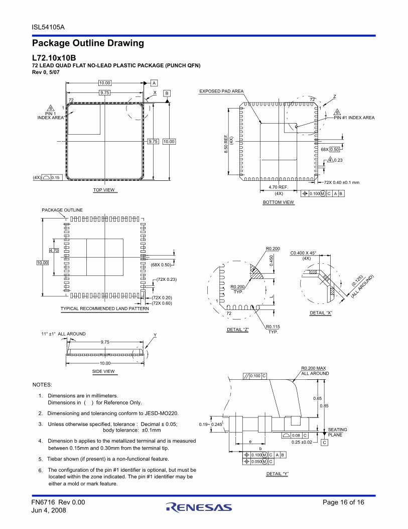
Package Outline Drawing
L72.10x10B72 LEAD QUAD FLAT NO-LEAD PLASTIC PACKAGE (PUNCH QFN)Rev 0, 5/07
BOTTOM VIEW
SIDE VIEW
TOP VIEW
C0.400 X 45°
11° ±1° ALL AROUND
e
b
L0.
450
8.50
RE
F.
4.70 REF.
(0.1
25)
68X
TYPICAL RECOMMENDED LAND PATTERN
PACKAGE OUTLINE
(4X)
INDEX AREA
6PIN 1
4
PIN #1 INDEX AREA6
R0.200 MAX ALL AROUND
(4X)
Y
1
72
0.100 C
DETAIL “Z” TYP.R0.115
TYP.R0.200
R0.200
1
72
EXPOSED PAD AREAX
A
(4X
)
(4X)
PLANESEATING
(ALL
ARO
UND)
Z72
1
0.19~ 0.245
10.00
10.00
9.75
(72X 0.60)
(68X 0.50)
(72X 0.20)
(72X 0.23)
4.70
9.75
10.00
0.85
0.65
0.23
0.50
72X 0.40 ±0.1 mm
B
9.75 10.00
B0.100 M AC
B0.100 M AC
0.050 M C
0.08 C
C0.25 ±0.02
DETAIL “X”
DETAIL “Y”
0.15
located within the zone indicated. The pin #1 identifier may be
Unless otherwise specified, tolerance : Decimal ± 0.05;
Tiebar shown (if present) is a non-functional feature.
The configuration of the pin #1 identifier is optional, but must be
between 0.15mm and 0.30mm from the terminal tip.Dimension b applies to the metallized terminal and is measured
Dimensions in ( ) for Reference Only.
Dimensioning and tolerancing conform to JESD-MO220.
6.
either a mold or mark feature.
3.
5.
4.
2.
Dimensions are in millimeters.1.
NOTES:
body tolerance: ±0.1mm