Embed Size (px)
Citation preview
AL5068S Designer’s Guide
No. AL5068S-E00-106 xmodus swiss GmbH Seite 1 / 25
ISDN Socket Modem
AL5068S, AL5068S-3V Series
Designer’s Guide
Version 106
Released 31. Dezember 2007
AL5068S Designer’s Guide
No. AL5068S-E00-106 xmodus swiss GmbH Seite 2 / 25
Information provided by xmodus swiss GmbH is believed to be accurate and reliable. However, no responsibility is assumed by xmodus swiss for its use, nor any infringement of patents or other rights of third parties which may result from its use. No license is granted by implication or otherwise under any patent rights of xmodus other than for circuitry embodied in xmodus products. Xmodus swiss reserves the right to change circuitry at any time without notice. This document is subject to change without notice. Product names or services listed in this publication are for identification purposes only, and may be trademarks or registered trademarks of their respective companies. All other marks mentioned herein are the property of their respective owners. © 2007 xmodus swiss GmbH Printed in Switzerland All Rights Reserved
AL5068S Designer’s Guide
No. AL5068S-E00-106 xmodus swiss GmbH Seite 3 / 25
TABLE OF CONTENTS 1. INTRODUCTION................................................................................................. 5
1.1 Overview ...................................................................................................... 5 1.2 Product description....................................................................................... 5 1.3 Features ....................................................................................................... 6 1.4 Command Sets and S-Registers .................................................................. 6
2. TECHNICAL OVERVIEW ................................................................................... 7 2.1 Dialing procedures ....................................................................................... 7 2.2 AT Commands ............................................................................................. 7
2.2.1 Configuration Commands ......................................................................... 7 2.2.2 AT Connection Commands....................................................................... 7
2.3 ISDN Protocols:............................................................................................ 8 2.4 Firmware Updates ........................................................................................ 8 2.5 Supported Interfaces .................................................................................... 8 2.7 Power consumption and power down modes............................................... 9 2.8 Command Sets and S-Registers .................................................................. 9
3. HARDWARE INTERFACE................................................................................ 10 3.1 Interface Signals......................................................................................... 10 3.2 Signal Descriptions..................................................................................... 10 3.3 S0 INTERFACE .......................................................................................... 16 3.4 External Reset Interface............................................................................. 17
3.4.1 Recommended Reset Circuit .................................................................. 17 3.5 IOM-2 Bus Interface ................................................................................... 18
4. DESIGN CONSIDERATIONS ........................................................................... 19 4.1 PC Board Layout Guidelines ...................................................................... 19
4.1.1 General................................................................................................... 19 4.1.2 Electromagnetic Interference (EMI) Considerations ............................... 20 4.1.3 Other Considerations.............................................................................. 20
4.2 Manufacturing Considerations.................................................................... 21 5. PACKAGE DIMENSIONS................................................................................. 22
6. SOCKET MODEM APPROVALS ..................................................................... 23 6.1 Considerations for Telecom Approvals....................................................... 23
6.1.1 ISDN Connection .................................................................................... 23 6.2 Considerations for Electrical Safety............................................................ 23
6.2.1 Conditions for Maintaining Safety Compliance. ...................................... 23 6.2.2 Power Supply [EN60950-1:2001, 1.6]..................................................... 23
6.3 Considerations for EMC ............................................................................. 24 6.3.1 EMC Compliance (EU Countries) ........................................................... 24 6.3.2 Installation in Host Systems (European Countries)................................ 24
7. Appendix A ...................................................................................................... 25 7.1 Schematic of external codecs .................................................................... 25
AL5068S Designer’s Guide
No. AL5068S-E00-106 xmodus swiss GmbH Seite 4 / 25
List of Figures
FIGURE 1-1. TYPICAL SERIAL BLOCK DIAGRAMS ................................................ 8
FIGURE 3.1 – SERIAL TTL PINOUT ....................................................................... 11
FIGURE 4-1. AL5068S SOCKET MODEM PHYSICAL DIMENSIONS ................... 22
List of Tables TABLE 3.1. SERIAL TTL SIGNALS................................................................................. 11 TABLE 3.2 / SIGNAL DESCRIPTIONS.............................................................................. 12 TABLE 3.3 / LED INTERFACE SIGNAL DESCRIPTIONS..................................................... 12 TABLE 3.4 / SERIAL INTERFACE SIGNAL DESCRIPTIONS.................................................. 13 TABLE 3.5 / DIGITAL ELECTRICAL CHARACTERISTICS ..................................................... 14 TABLE 3.6 / ABSOLUTE MAXIMUM RATINGS................................................................... 15
AL5068S Designer’s Guide
No. AL5068S-E00-106 xmodus swiss GmbH Seite 5 / 25
1. INTRODUCTION 1.1 Overview
This Designer’s Guide describes the hardware for the following ISDN socket modems of xmodus swiss GmbH: AL5068S ISDN Socket Modem (5V Version) AL5068S-3V ISDN Socket Modem (3V Version) AL5068SI-3V ISDN Socket Modem (3V Version and IOM-2 bus) The description apply to all these isdn-modems with any differences between product families noted. Refer to Modem Firmware Release notes for commands applicable to modem firmware. AT commands and S registers are defined in the AT Command Reference Manual.
1.2 Product description
The xmodus AL5068S and AL5068SI-3V Socket Modem Family provides the OEM with a complete ISDN data/voice/speakerphone modem in a compact socket-mountable module. This modules enables any devices to send and receive data over the ISDN network. The European EuroISDN DSS-1 ISDN network is supported. The module is fully approved and homologated and conforms to the CE regulations. This gives fastest time-to-market to ISDN-enable any devices. The compact size and high level of integration of the Socket Modem minimizes real estate and cost for motherboard and box modem applications. Its low power consumption makes it ideal for a wide variety of embedded control applications. The pin compatibility between the full range of Analog Series Socket Modems, ISDN and GSM Socket Modems allows upgrading and production configurability without hardware changes. As a data modem, the AL5068S Socket Modem can send and receive data at speeds up to 64kbps and 128kbps in the 2-channel version. B-Channel protocols such as V.110, V.120, PPP, transparent and X.75 are supported. For X.25 networks, X.31 Case A and X.31 Case B (D- and B-channel) is supported. The integrated X.3 PAD can be used for data transfer to the X.25 network. The AL5068SI-3V Socket Modem supports Voice features. By adding two external PCM Codecs the modem supports two independent analog voice ports. Digital voice transfer is also supported.
AL5068S Designer’s Guide
No. AL5068S-E00-106 xmodus swiss GmbH Seite 6 / 25
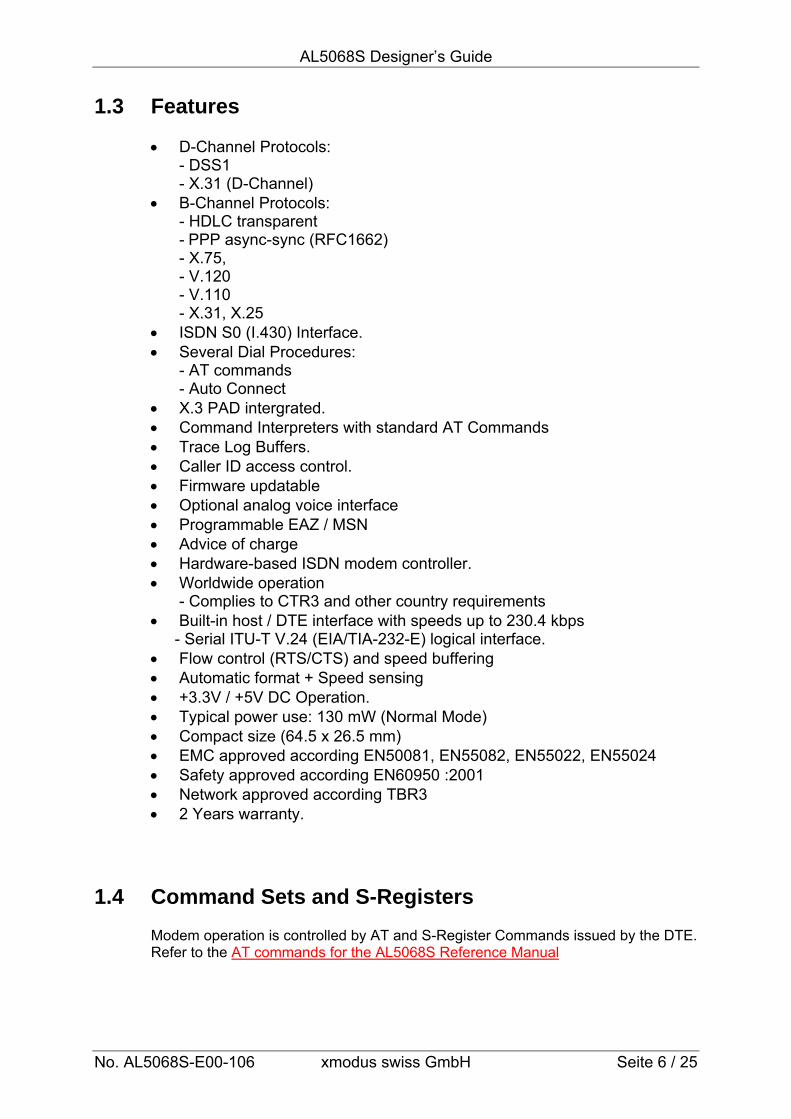
1.3 Features
• D-Channel Protocols: - DSS1 - X.31 (D-Channel) • B-Channel Protocols: - HDLC transparent - PPP async-sync (RFC1662) - X.75, - V.120 - V.110 - X.31, X.25 • ISDN S0 (I.430) Interface. • Several Dial Procedures: - AT commands - Auto Connect • X.3 PAD intergrated. • Command Interpreters with standard AT Commands • Trace Log Buffers. • Caller ID access control. • Firmware updatable • Optional analog voice interface • Programmable EAZ / MSN • Advice of charge • Hardware-based ISDN modem controller. • Worldwide operation - Complies to CTR3 and other country requirements • Built-in host / DTE interface with speeds up to 230.4 kbps - Serial ITU-T V.24 (EIA/TIA-232-E) logical interface. • Flow control (RTS/CTS) and speed buffering • Automatic format + Speed sensing • +3.3V / +5V DC Operation. • Typical power use: 130 mW (Normal Mode) • Compact size (64.5 x 26.5 mm) • EMC approved according EN50081, EN55082, EN55022, EN55024 • Safety approved according EN60950 :2001 • Network approved according TBR3 • 2 Years warranty.
1.4 Command Sets and S-Registers
Modem operation is controlled by AT and S-Register Commands issued by the DTE. Refer to the AT commands for the AL5068S Reference Manual
AL5068S Designer’s Guide
No. AL5068S-E00-106 xmodus swiss GmbH Seite 7 / 25
2. TECHNICAL OVERVIEW 2.1 Dialing procedures
The following dial procedures are supported: • AT commands • Auto-connect (Hotline call) • X.3 PAD
2.2 AT Commands
Via AT-Commands you may control the ISDN connections and change the configuration of the AL5068S. ISDN specific configuration commands are supported.
2.2.1 Configuration Commands
A range of parameters can be controlled by the configuration commands of the AL5068S as listed below: • Setting own msn number • Recommended B channel protocol • Serial Interface Parameters (baud rate, flow control, etc.) • AT / Auto-connect operation mode • Firmware download
2.2.2 AT Connection Commands
Command Function Response ATDxxx Establishes an ISDN connection CONNECT ATH Disconnects an ISDN connection OK
Whenever the ISDN connection with a communication partner is established, a transparent channel for serial data is provided. A detailed description of the AT-Commands is found in the AT-Command manual for the socket modem AL5068S.
AL5068S Designer’s Guide
No. AL5068S-E00-106 xmodus swiss GmbH Seite 8 / 25
2.3 ISDN Protocols:
ISDN Channel Protocols
D-channel protocols: DSS1 X.31 D-channel
B-channel protocols:
HDLC (transparent) PPP sync-async (RFC 1662) X.75 Bit-transparent X.31 / X.25 V.110 V.120
2.4 Firmware Updates
Firmware updates can always be affected via the local serial interface. 2.5 Supported Interfaces
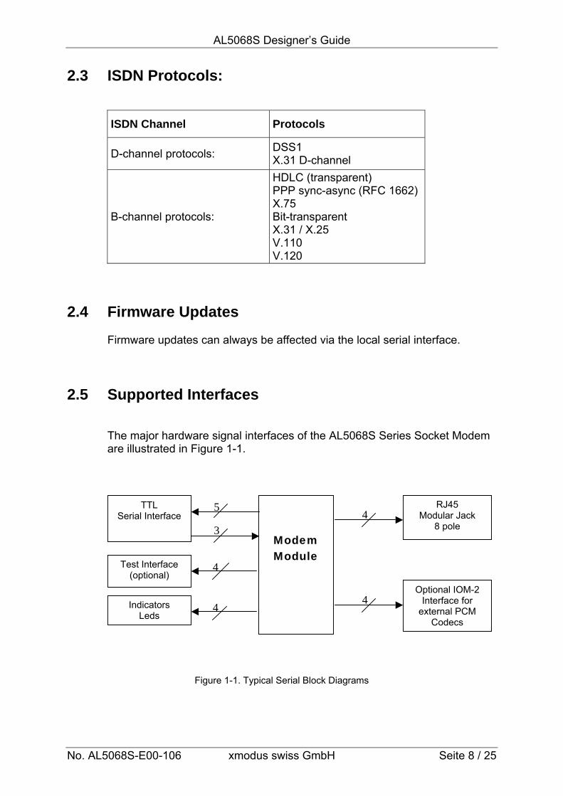
The major hardware signal interfaces of the AL5068S Series Socket Modem are illustrated in Figure 1-1.
Figure 1-1. Typical Serial Block Diagrams
Modem Module
TTL Serial Interface
Indicators Leds
RJ45 Modular Jack
8 pole
5
3
4
4
Optional IOM-2Interface for
external PCM Codecs
4
Test Interface (optional)
4

AL5068S Designer’s Guide
No. AL5068S-E00-106 xmodus swiss GmbH Seite 9 / 25
Serial / Indicator Interface:
DTE serial interface and indicator outputs are supported.
Serial Interface: 8-line TTL logic serial interface to the DTE is supported.
LED Interface: Four direct connect LED indicator outputs are supported
The terminal (DTE) baudrate is determined automatically by the MCU firmware. It provides autobaud from 9600bps to 115200bps.
The terminal (DTE) character format is fixed to 8 bits, no parity and 1 stop bit. There is no setting required for the DTE character format.
ISDN Line Interface: The AL5068S Socket Modem family connects to the ISDN network S0 Interface (spec. I.430). It supports the EDSS-1 (EuroISDN) protocol stack for network access.
IOM-2 Interface:
The AL5068SI-3V modem provides the IOM-2 bus. External PCM codecs can be connected to use analog voice interfaces (see application notes).
2.7 Power consumption and power down modes
To reduce power consumption of the AL5068S, a power down mode can be activated by the AL5068S. The following values are approximate power consumption values in the different states:
Condition Power usage
Power down ~ TBD ISDN active ~ 27 mA
2.8 Command Sets and S-Registers
Modem operation is controlled by AT and S-Register Commands issued by the DTE. Refer to the AT commands for the AL5068S Modem Reference Manual
AL5068S Designer’s Guide
No. AL5068S-E00-106 xmodus swiss GmbH Seite 10 / 25
3. HARDWARE INTERFACE 3.1 Interface Signals
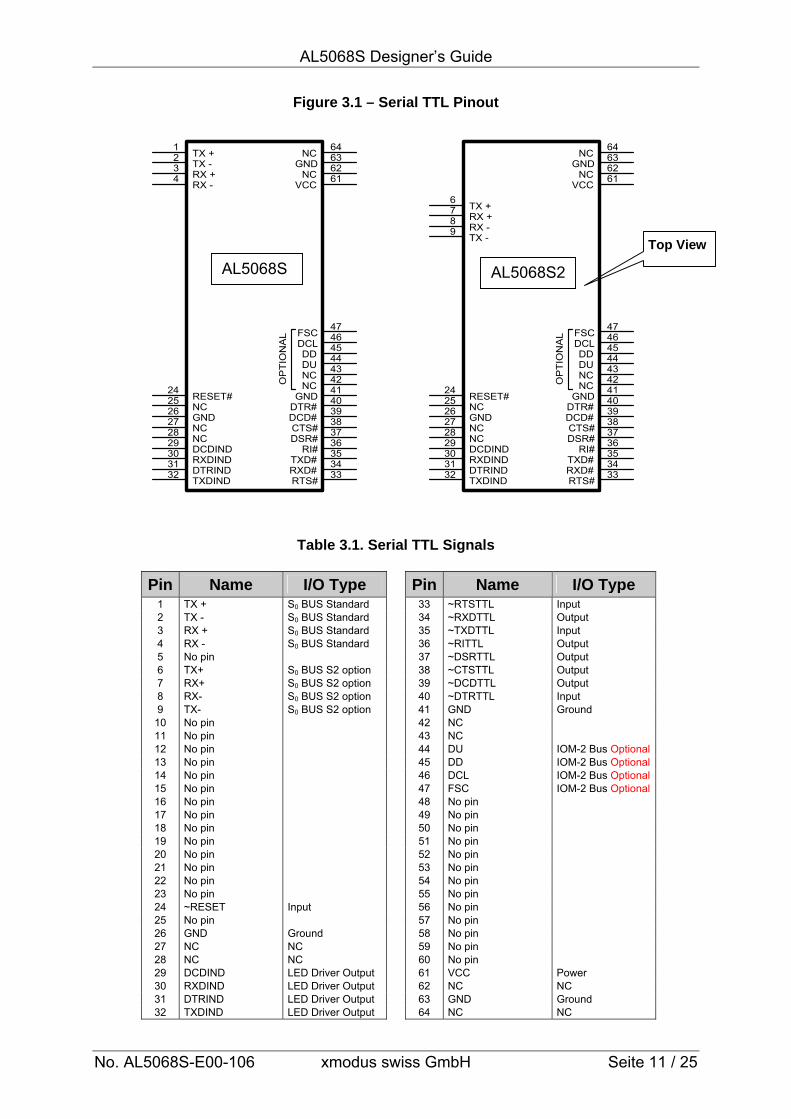
The ISDN Socket Modem pin assignments with DTE serial TTL interface are shown in Figure 3-1 and are listed in Table 3-1.
3.2 Signal Descriptions
The Socket Modem interface signals are described in Table 3.2, 3.3 and 3.4. The digital electrical characteristics are listed in Table 3.5 The absolut maximum ratings are listed in Table 3-6.
AL5068S Designer’s Guide
No. AL5068S-E00-106 xmodus swiss GmbH Seite 11 / 25
Figure 3.1 – Serial TTL Pinout
Table 3.1. Serial TTL Signals
Pin Name I/O Type Pin Name I/O Type 1 TX + S0 BUS Standard 33 ~RTSTTL Input 2 TX - S0 BUS Standard 34 ~RXDTTL Output 3 RX + S0 BUS Standard 35 ~TXDTTL Input 4 RX - S0 BUS Standard 36 ~RITTL Output 5 No pin 37 ~DSRTTL Output 6 TX+ S0 BUS S2 option 38 ~CTSTTL Output 7 RX+ S0 BUS S2 option 39 ~DCDTTL Output 8 RX- S0 BUS S2 option 40 ~DTRTTL Input 9 TX- S0 BUS S2 option 41 GND Ground
10 No pin 42 NC 11 No pin 43 NC 12 No pin 44 DU IOM-2 Bus Optional 13 No pin 45 DD IOM-2 Bus Optional 14 No pin 46 DCL IOM-2 Bus Optional 15 No pin 47 FSC IOM-2 Bus Optional 16 No pin 48 No pin 17 No pin 49 No pin 18 No pin 50 No pin 19 No pin 51 No pin 20 No pin 52 No pin 21 No pin 53 No pin 22 No pin 54 No pin 23 No pin 55 No pin 24 ~RESET Input 56 No pin 25 No pin 57 No pin 26 GND Ground 58 No pin 27 NC NC 59 No pin 28 NC NC 60 No pin 29 DCDIND LED Driver Output 61 VCC Power 30 RXDIND LED Driver Output 62 NC NC 31 DTRIND LED Driver Output 63 GND Ground 32 TXDIND LED Driver Output 64 NC NC
Top View
NC 42
TXDIND32
DTR# 40
RX +7
NC64
NC62
RESET#24
DU44
OP
TIO
NA
L
TXD#35
RTS# 33
NC27
DCL46
DSR#37
DCDIND29
DCD#39
DTRIND31
GND41
NC25
RX -8
GND 63
TX -9
NC 43
TX +6
VCC 61
RXD#34
GND26
DD 45
NC28
RI# 36
FSC 47
CTS# 38
RXDIND30
NC25
DCD#39
GND41
DU44
DTRIND31
DSR#37
TXD#35
RX -4
OP
TIO
NA
L
DCDIND29
RTS# 33
NC27
RESET#24
NC62
DD 45
TX +1
NC 43
NC64
NC 42
TXDIND32
CTS# 38
FSC 47
RXDIND30 RI# 36
DTR# 40
RXD#34
NC28
RX +3
DCL46
GND26
VCC 61TX -2 GND 63
AL5068S AL5068S2
AL5068S Designer’s Guide
No. AL5068S-E00-106 xmodus swiss GmbH Seite 12 / 25
Table 3.2 / Signal Descriptions
Label I/O Type Signal Name Description
VCC PWR +5 VDC / 3.3 VDC
GND GND Ground. Connect to Digital Ground on the interface circuit.
~RESET IC
Modem Reset. The Active Low ~RESET input resets the Socket Modems logic and returns the AT command set to the original factory default values and to “stored values” in NVRAM. ~RESET is connected to a built-in reset circuit on the Socket Modem. This input is 5V tolerant.
TX+ S0 Bus Transmit Positive from ISDN S0 Bus.
TX - S0 Bus Transmit Negative from ISDN S0 Bus.
RX + S0 Bus Receive Positive from ISDN S0 Bus.
RX - S0 Bus Receive Negative from ISDN S0 Bus.
Table 3.3 / LED Interface Signal Descriptions
Label I/O Type Signal Name/Description
LED driver lines are open-drain inverter-driven (74HCT05) lines with 1.5 KΩ, 1/10W pull-up resistors.
DCDIND OG Active High DCD Status
RXDIND OG Active High RXD Status DTRIND OG Active High DTR Status
TXDIND OG Active High TXD Status
AL5068S Designer’s Guide
No. AL5068S-E00-106 xmodus swiss GmbH Seite 13 / 25
Table 3.4 / Serial Interface Signal Descriptions
~RTSTTL IA
Request To Send (TTL Active Low). ~RTS is used to condition the local modem for data transmission and, during half-duplex operation, to control the direction of data transmission. On a full-duplex channel, RTS-OFF maintains the modem in a non-transmit mode. A non-transmit mode does not imply that the ISDN link have been terminated. RTS input ON causes the modem to transmit data on TXD when ~CTS becomes active.
~RXDTTL OA
Received Data (TTL Active Low). The modem uses the ~RXD line to send data received from the ISDN line to the DTE and to send modem responses to the DTE. During command mode, ~RXD data represents the modem responses to the DTE. Modem responses take priority over incoming data when the two signals are in competition for ~RXD.
~TXDTTL IA
Transmitted Data (Active Low). The DTE uses the ~TXD line to send data to the modem for transmission over the ISDN network or to transmit commands to the modem. The DTE should hold this circuit in the mark state when no data is being transmitted or during intervals between characters.
~CTSTTL OA
Clear To Send (TTL Active Low). ~CTS is controlled by the modem to indicate whether or not the modem is ready to transmit data. ~CTS ON, together with the ~RTS ON, ~DSR ON, and ~DTR ON (where implemented), indicates to the DTE that signals presented on TXD will be transmitted to the ISDN network. ~CTS OFF indicates to the DTE that it should not transfer data across the interface on TXD. ~CTS ON is a response to ~DTR ON and ~RTS, delayed as may be appropriate for the modem to establish an ISDN connection.
~RITTL OA Ring Indicate (TTL Active Low). ~RI output ON (low) indicates the presence of ALERTING on the ISDN network.
~DSRTTL OA Data Set Ready (TTL Active Low). ~DSR indicates modem status to the DTE. ~DSR OFF (high) indicates that the DTE is to disregard all signals appearing on the interchange circuits except Ring Indicator (~RI).
~DCDTTL OA Data Carrier Detect (TTL Active Low). ~DCD output is ON (low) when a link is established over the ISDN network and is OFF (high) when no link is present.
~DTRTTL IA
Data Terminal Ready (TTL Active Low). The ~DTR input is turned ON (low) by the DTE when the DTE is ready to transmit or receive data. ~DTR ON prepares the modem to be connected to the ISDN network, and maintains the connection established by the DTE (manual answering) or internally (automatic answering). ~DTR OFF places the modem in the disconnect state under control of the AT Command AT&Dx
AL5068S Designer’s Guide
No. AL5068S-E00-106 xmodus swiss GmbH Seite 14 / 25
Table 3.5 / Digital Electrical Characteristics
Parameter Symbol Min. Typ. Max. Units Test Condition
Input Voltage Type IA Type IC
VI
0 0
- -
5.5 5.5
Vdc
5V tolerant 5V tolerant
Output Voltage Type IA Type IC
VI
0 0
- -
3.3 3.3
Vdc
Input High Voltage Type IA Type IC
VICH
2.0 2.0
- -
- -
Vdc
Input Low Voltage Type IA Type IC
VIL
- -
- -
0.8 0.8
Vdc
Output High Voltage Type OA Type OG
VOH
2.8 2.4
- -
-
VCC
Vdc
ILOAD = -4.0 mA ILOAD = -1.0 mA
Output Low Voltage Type OA Type OG
VOL
- -
- -
0.4 0.4
Vdc
ILOAD = 4.0 mA ILOAD = 1.0 mA
Three-State Leakage Current 3.3 / 0.5V
ITSI -
-
3 μADC
VIN = 3.3(0.5V
Circuit Types Type IA Type IC Type OA
TTL ~RESET
TTL with 3state
Notes: 1. Test Conditions: VCC = +/- 5%, TA = o° to 70°C, Vcc = 3.3V +/- 5%
AL5068S Designer’s Guide
No. AL5068S-E00-106 xmodus swiss GmbH Seite 15 / 25
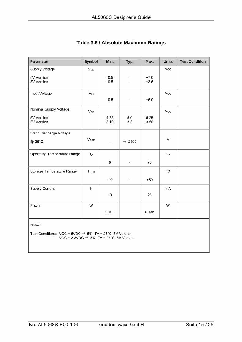
Table 3.6 / Absolute Maximum Ratings Parameter Symbol Min. Typ. Max. Units Test Condition
Supply Voltage 5V Version 3V Version
VDD
-0.5 -0.5
- -
+7.0 +3.6
Vdc
Input Voltage
VIN
-0.5
-
+6.0
Vdc
Nominal Supply Voltage 5V Version 3V Version
VDD
4.75 3.10
5.0 3.3
5.25 3.50
Vdc
Static Discharge Voltage @ 25°C
VESD -
+/- 2500
V
Operating Temperature Range
TA
0
-
70
°C
Storage Temperature Range
TSTG
-40
-
+80
°C
Supply Current
ID
19
26
mA
Power
W
0.100
0.135
W
Notes: Test Conditions: VCC = 5VDC +/- 5%, TA = 25°C, 5V Version VCC = 3.3VDC +/- 5%, TA = 25°C, 3V Version
AL5068S Designer’s Guide
No. AL5068S-E00-106 xmodus swiss GmbH Seite 16 / 25
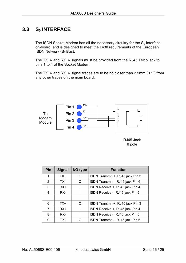
3.3 S0 INTERFACE
The ISDN Socket Modem has all the necessary circuitry for the S0 Interface on-board, and is designed to meet the I.430 requirements of the European ISDN Network (S0 Bus). The TX+/- and RX+/- signals must be provided from the RJ45 Telco jack to pins 1 to 4 of the Socket Modem. The TX+/- and RX+/- signal traces are to be no closer than 2.5mm (0.1”) from any other traces on the main board.
Pin Signal I/O type Function 1 TX+ O ISDN Transmit +, RJ45 jack Pin 3 2 TX- O ISDN Transmit -, RJ45 jack Pin 6 3 RX+ I ISDN Receive +, RJ45 jack Pin 4 4 RX- I ISDN Receive -, RJ45 jack Pin 5
6 TX+ O ISDN Transmit +, RJ45 jack Pin 3 7 RX+ I ISDN Receive +, RJ45 jack Pin 4 8 RX- I ISDN Receive -, RJ45 jack Pin 5 9 TX- O ISDN Transmit -, RJ45 jack Pin 6
8 7 6 5 4 3 2 1
Pin 1
Pin 2
Pin 3
Pin 4
To Modem Module
RJ45 Jack 8 pole
TX+
TX-
RX+
RX-
AL5068S Designer’s Guide
No. AL5068S-E00-106 xmodus swiss GmbH Seite 17 / 25
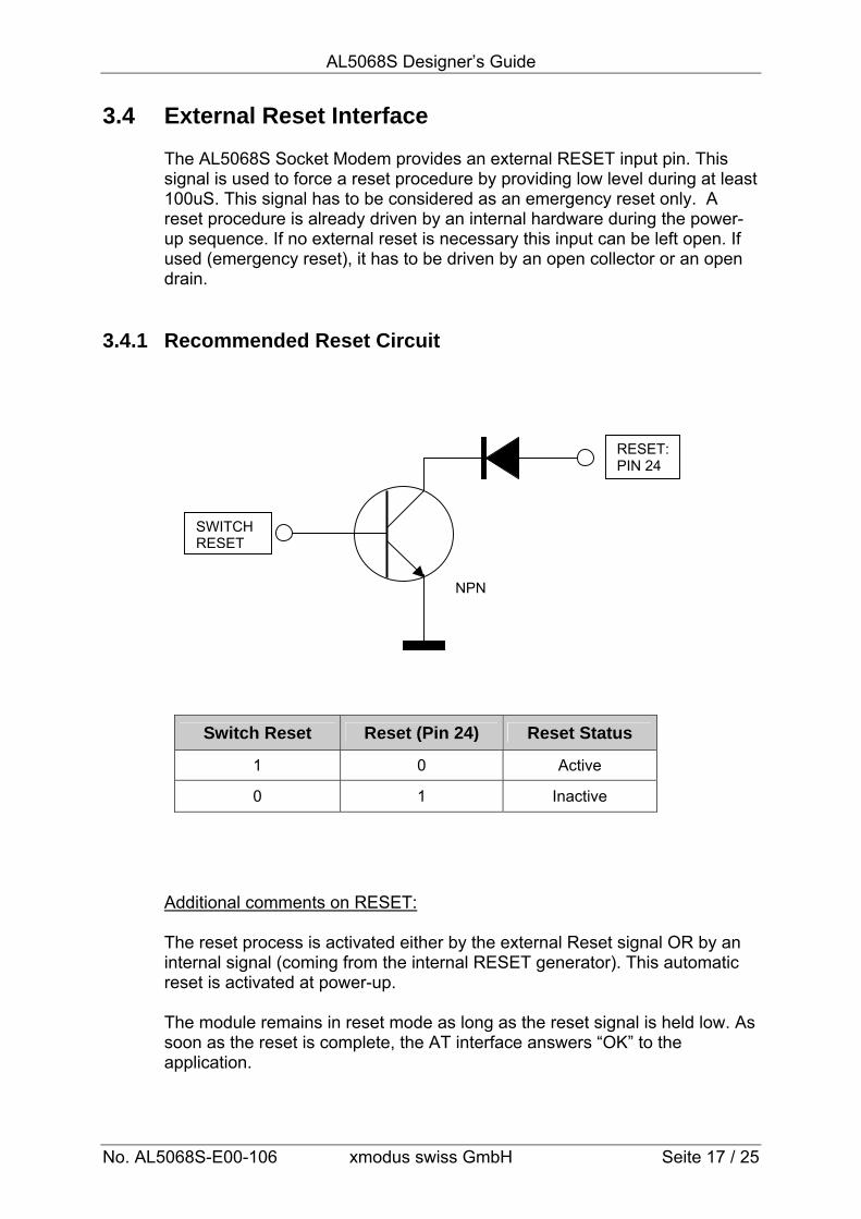
3.4 External Reset Interface
The AL5068S Socket Modem provides an external RESET input pin. This signal is used to force a reset procedure by providing low level during at least 100uS. This signal has to be considered as an emergency reset only. A reset procedure is already driven by an internal hardware during the power-up sequence. If no external reset is necessary this input can be left open. If used (emergency reset), it has to be driven by an open collector or an open drain.
3.4.1 Recommended Reset Circuit
Switch Reset Reset (Pin 24) Reset Status
1 0 Active
0 1 Inactive
Additional comments on RESET: The reset process is activated either by the external Reset signal OR by an internal signal (coming from the internal RESET generator). This automatic reset is activated at power-up. The module remains in reset mode as long as the reset signal is held low. As soon as the reset is complete, the AT interface answers “OK” to the application.
SWITCH RESET
RESET:PIN 24
NPN
AL5068S Designer’s Guide
No. AL5068S-E00-106 xmodus swiss GmbH Seite 18 / 25
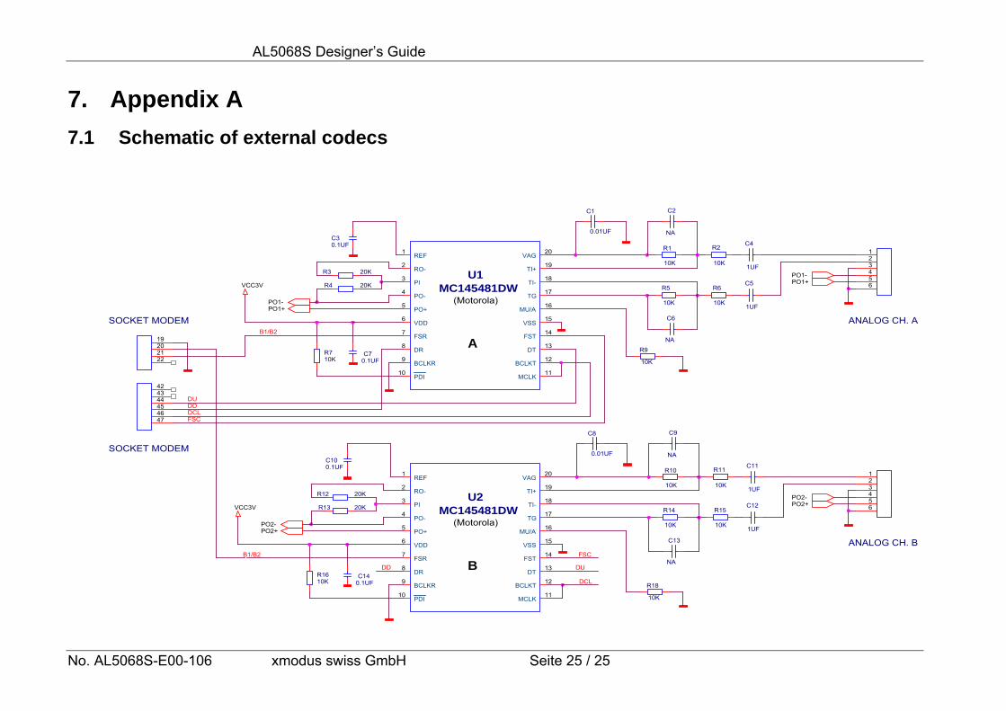
3.5 IOM-2 Bus Interface
The AL5068SI-3V ISDN Modem supports 2 independent analog channels by adding 2 external PCM Codecs. This Codecs are connected to the IOM-2 bus on pins 44…47 of the socket modem. It is possible to setup 2 simultaneous links for both incoming and outgoing calls. The serial port remains in command state in this mode. The 2 external Codecs are marked with Codec A and Codec B. Each Codec (A or B) can have his own MSN. Each call can therefore be directed to a specific Codec. There are 2 additional I/O signals to drive the B-Channel source of each Codec. Please refer to the “AL5068S AT Commands Reference Manual”, chapter 9 for a detailed description of all the AT commands regarding the voice modes.
For a detailed schematic refer to Appendix A in this manual.
AL5068S Designer’s Guide
No. AL5068S-E00-106 xmodus swiss GmbH Seite 19 / 25
4. DESIGN CONSIDERATIONS
Good engineering practices must be adhered to when designing a printed circuit board (PCB) containing the AL5068S Socket Modem module. Suppression of noise is essential to the proper operation and performance of the modem itself and for surrounding equipment. Two aspects of noise in an OEM board design containing the AL5068S Socket Modem module must be considered: on-board/off-board generated noise that can affect analog signal levels and analog-to-digital conversion (ADC) / digital-to-analog conversion (DAC), and on-board generated noise that can radiate off-board. Both on-board and off-board generated noise that is coupled on-board can affect interfacing signal levels and quality, especially in low level analog signals. Of particular concern is noise in frequency ranges affecting modem performance. On-board generated electromagnetic interference (EMI) noise that can be radiated or conducted off-board is a separate, but equally important concern. This noise can affect the operation of surrounding equipment. Most local government agencies have stringent certification requirements that must be met for use in specific environments. Proper PC board layout (component placement, signal routing, trace thickness and geometry, etc.) , component selection (composition, value, and tolerance), interface connections, and shielding are required for the board design to achieve desired modem performance and to attain certification. The aspects of proper engineering practices are beyond the scope of this designer’s guide. The designer should consult noise suppression techniques described in technical publications and journals, electronics and electrical engineering text books, and component supplier application notes. Technical and professional associations as well as component suppliers often offer seminars addressing noise suppression techniques.
4.1 PC Board Layout Guidelines 4.1.1 General
1. In a 4-layer design, provide an adequate ground plane covering the entire board. Socket Modem DGND and AGND pins are tied together on the Socket Modem.
2. As a general rule, route digital signals on the component side of the PCB and the
analog signals on the solder side. The sides may be reversed to match particular OEM requirements. Route the digital traces perpendicular to the analog traces to minimize signal cross coupling.
3. Route the modem signals to provide maximum isolation between noise sources and
noise sensitive inputs. When layout requirements necessitate routing these signals together, they should be separated by neutral signals.
4. All power and ground traces should be at least 0.05 in. wide. 5. ISDN S0 signal traces are to be no closer than 2.5mm (0.1") from any other traces for
European applications.
6. If the Socket Modem is mounted flush with the host PCB, the host PCB should be clear of all traces directly underneath the Socket Modem oscillator section. It is strongly suggested that the Socket Modem is mounted at least 0.130 inch above the host board. (See section 4.4)
AL5068S Designer’s Guide
No. AL5068S-E00-106 xmodus swiss GmbH Seite 20 / 25
4.1.2 Electromagnetic Interference (EMI) Considerations
The following guidelines are offered to specifically help minimize EMI generation. Some of these guidelines are the same as, or similar to, the general guidelines but are mentioned again to reinforce their importance. In order to minimize the contribution of the Socket Modem-based design to EMI, the designer must understand the major sources of EMI and how to reduce them to acceptable levels.
1. Keep traces carrying high frequency signals as short as possible. 2. Provide a good ground plane or grid. In some cases, a multilayer board may be required
with full layers for ground and power distribution. 3. Decouple power from ground with decoupling capacitors as close to the Socket Modem
module power pins as possible. 4. Eliminate ground loops, which are unexpected current return paths to the power source
and ground. 5. Decouple the power cord at the power cord interface with decoupling capacitors.
Methods to decouple power lines are similar to decoupling telephone lines. 7. Locate high frequency circuits in a separate area to minimize capacitive coupling to
other circuits. 8. Locate cables and connectors so as to avoid coupling from high frequency circuits. 10. If a multilayer board design is used, make no cuts in the ground or power planes and be
sure the ground plane covers all traces. 11. Minimize the number of through-hole connections on traces carrying high frequency
signals. 12. Avoid right angle turns on high frequency traces. Forty-five degree corners are good,
however, radius turns are better 13. On 2-layer boards with no ground grid, provide a shadow ground trace on the opposite
side of the board to traces carrying high frequency signals. This will be effective as a high frequency ground return if it is three times the width of the signal traces.
14. Distribute high frequency signals continuously on a single trace rather than several
traces radiating from one point. 4.1.3 Other Considerations
The pins of all Socket Modems are grouped according to function. The ISDN interface, Host interface, and LED interface pins are all conveniently arranged, easing the host board layout design. Xmodus has tested the AL5068S Socket Modems for compliance with CTR3. The certificates apply only to designs that route the ISDN signals (pins 1 to 4) directly to the RJ45 jack.
AL5068S Designer’s Guide
No. AL5068S-E00-106 xmodus swiss GmbH Seite 21 / 25
4.2 Manufacturing Considerations
The Socket Modem has been designed to be mounted onto the host board in one of two ways. The first method consists of soldering two 32-pin strip sockets to the host board and inserting the Socket Modem into the sockets. A suggested part number for the 32-pin socket is Sam Tec SMM-132-01-F-S. The second way is to solder the Socket Modem directly to the host board. The most efficient way to do this is through a wave solder process. The recommended hole size for the Socket Modem pins is 0.036 in. ±0.003 in. in diameter. Spacers can be used to hold the Socket Modem vertically in place during the wave solder process. A spacer should be placed on pin 32 and pin 64 of the Socket Modem. A suggested part number for the spacer is BIVAR 938-0.130 for P1(0.310in) option Socket Modems. The spacers can be left on permanently and will not effect operation. Socket Modems can be put through a water wash process.
AL5068S Designer’s Guide
No. AL5068S-E00-106 xmodus swiss GmbH Seite 22 / 25
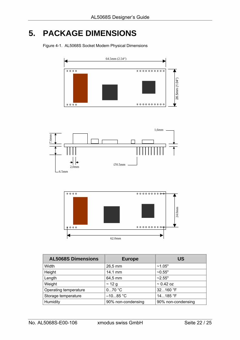
5. PACKAGE DIMENSIONS
Figure 4-1. AL5068S Socket Modem Physical Dimensions
AL5068S Dimensions Europe US Width 26,5 mm ~1.05" Height 14.1 mm ~0.55" Length 64,5 mm ~2.55" Weight ~ 12 g ~ 0.42 oz Operating temperature 0...70 °C 32...160 °F Storage temperature –10...85 °C 14...185 °F Humidity 90% non-condensing 90% non-condensing
26.5
mm
(1.0
4“)
64.5mm (2.54“)
24.
0mm
62.0mm
7,6m
m
6,5mm 2,0mm
∅0.5mm
1,6mm
AL5068S Designer’s Guide
No. AL5068S-E00-106 xmodus swiss GmbH Seite 23 / 25
6. SOCKET MODEM APPROVALS
The Socket Modem module is approved as a host-independent modem card. To maintain type approvals, permits and/or licenses valid, the guidelines described in this document must be followed.
6.1 Considerations for Telecom Approvals The Socket Modem has been assessed and has been found to comply with the relevant harmonized standards as defined by the European ETSI Directive (ETSI TC-TE).
These standards are: TBR3 / CTR3
6.1.1 ISDN Connection
The Socket Modem can be connected to the S0 Bus of the ISDN Telephone Network either a) by using a 4-wire flying cable to connect pins 1 to 4 of the module to an RJ-45
connector which can be assembled in a suitable location of the host system enclosure, OR b) by providing traces on the host system motherboard for the ISDN connection signals
between the card and an RJ-45 connector
If connection option a) is used, the cable and its installation inside the host system must be in accordance with the guidelines in IEC950/EN60950 (e.g. the insulation material must withstand electric strength tests as described in section 3.4).
If connection option b) is used, NO additional components must be connected to the S0-Bus signals. Other components not intended for use with this design may affect the network access characteristics of the modem and may therefore invalidate the type approvals, permits and/or licences. In both cases, for the connection between the host and the PSTN wall connector, a cable with RJ-45 modular jack and an appropriate national plug must be used.
6.2 Considerations for Electrical Safety 6.2.1 Conditions for Maintaining Safety Compliance.
The Socket Modem has been assessed with respect to electrical safety and has been found to comply with relevant standards as defined by the European Low Voltage Directive (72/23EEC). The particular standard is EN 60950-1:2001. The card is rated as Class III equipment and it is intended for use in Pollution Degree 2 environments only [see EN60950-1:2001, 2.10.4]. Material Group IIIa or IIIb (Comparative Tracking Index below 400 according o IEC 112, method A) is assumed for any host system PCB that has traces and/or circuitry with TNV potential.
It is assumed that the modem card will only be assembled in a host system unit that complies with IEC60950/EN60950. Some particular requirements are [see EN60950-1:2001, 2.1.1, 2.2, 2.3, 2.9, 2.10 and 4.7.3.2]:
6.2.2 Power Supply [EN60950-1:2001, 1.6]
Before installing the Socket Modem in a host system, the installer must ensure that the power drawn by the card, together with the host and any auxiliary cards drawing power from the host, is within the rating of the host power supply unit. The Socket Modem's power consumption is typically 0.15 W (@ 5.0 Vdc).
AL5068S Designer’s Guide
No. AL5068S-E00-106 xmodus swiss GmbH Seite 24 / 25
6.3 Considerations for EMC
6.3.1 EMC Compliance (EU Countries) The Socket Modem has been assessed with respect to emission of and immunity to electromagnetic disturbances and has been found to comply with the relevant harmonized standards as defined by the European EMC Directive (89/336/EEC). These standards are: • Generic emission standards which refers to
EN 55022:1998 +A1:2000, Class B
• Generic immunity standards which refers to EN 55024:1999
6.3.2 Installation in Host Systems (European Countries)
It is assumed that the Socket Modem will only assembled in host systems that comply with the EMC Directive. As per definition of the EMC Directive, the card and its host system will constitute an "installation" similar to e.g. a PC card modem installed in a personal computer. Therefore, if the host system complies with the EMC Directive, there should be no need for verifying continued compliance of the complete system. However, note that it is the responsibility of the professional installer of Socket Modem to ensure that the complete system placed on the market complies with the Directive.
AL5068S Designer’s Guide
No. AL5068S-E00-106 xmodus swiss GmbH Seite 25 / 25
7. Appendix A
7.1 Schematic of external codecs
R6
10K
B1/B2
C4
1UF
R9
10K
C1
0.01UF
C11
1UF
U1MC145481DW
1
2
3
4
5
6
7
8
9
10
20
19
18
17
16
15
14
13
12
11
REF
RO-
PI
PO-
PO+
VDD
FSR
DR
BCLKR
PDI
VAG
TI+
TI-
TG
MU/A
VSS
FST
DT
BCLKT
MCLK
(Motorola)
DD
C12
1UF
C8
0.01UF
PO1+PO1-
DD
R15
10K
R4 20K
R3 20K
C9
NA
U2MC145481DW
1
2
3
4
5
6
7
8
9
10
20
19
18
17
16
15
14
13
12
11
REF
RO-
PI
PO-
PO+
VDD
FSR
DR
BCLKR
PDI
VAG
TI+
TI-
TG
MU/A
VSS
FST
DT
BCLKT
MCLK
SOCKET MODEM
19202122
R10
10K
R11
10K
PO2+
B
R14
10K
VCC3V
R12 20K
R1
10K
DCL
C13
NA
VCC3V
B1/B2
A
C30.1UF
C6
NA
PO2-
FSC
PO2-
C140.1UF
R2
10K
DU
ANALOG CH. B
123456
R710K
C5
1UF
FSC
R1610K
C70.1UF
C2
NA
ANALOG CH. A
123456R5
10K
DU
C100.1UF
(Motorola)
R13 20K
SOCKET MODEM
424344454647
PO2+
DCL
PO1-
R18
10K
PO1+


![Cis TelePresenCo Ce isDn link...ISDN PRI Interface 1 testShutdown ISDN BRI Interface [1..4] testLoopmode ISDN BRI Interface [1..4] testPattern Cisco telePresence ISDN Link Administrator](https://img.pdfslide.us/doc/110x75/6131c5191ecc51586944f1c2/cis-telepresenco-ce-isdn-link-isdn-pri-interface-1-testshutdown-isdn-bri-interface.jpg)