Embed Size (px)
Citation preview

To learn more about ON Semiconductor, please visit our website at www.onsemi.com
Is Now Part of
ON Semiconductor and the ON Semiconductor logo are trademarks of Semiconductor Components Industries, LLC dba ON Semiconductor or its subsidiaries in the United States and/or other countries. ON Semiconductor owns the rights to a number of patents, trademarks, copyrights, trade secrets, and other intellectual property. A listing of ON Semiconductor’s product/patent coverage may be accessed at www.onsemi.com/site/pdf/Patent-Marking.pdf. ON Semiconductor reserves the right to make changes without further notice to any products herein. ON Semiconductor makes no warranty, representation or guarantee regarding the suitability of its products for any particular purpose, nor does ON Semiconductor assume any liability arising out of the application or use of any product or circuit, and specifically disclaims any and all liability, including without limitation special, consequential or incidental damages. Buyer is responsible for its products and applications using ON Semiconductor products, including compliance with all laws, regulations and safety requirements or standards, regardless of any support or applications information provided by ON Semiconductor. “Typical” parameters which may be provided in ON Semiconductor data sheets and/or specifications can and do vary in different applications and actual performance may vary over time. All operating parameters, including “Typicals” must be validated for each customer application by customer’s technical experts. ON Semiconductor does not convey any license under its patent rights nor the rights of others. ON Semiconductor products are not designed, intended, or authorized for use as a critical component in life support systems or any FDA Class 3 medical devices or medical devices with a same or similar classification in a foreign jurisdiction or any devices intended for implantation in the human body. Should Buyer purchase or use ON Semiconductor products for any such unintended or unauthorized application, Buyer shall indemnify and hold ON Semiconductor and its officers, employees, subsidiaries, affiliates, and distributors harmless against all claims, costs, damages, and expenses, and reasonable attorney fees arising out of, directly or indirectly, any claim of personal injury or death associated with such unintended or unauthorized use, even if such claim alleges that ON Semiconductor was negligent regarding the design or manufacture of the part. ON Semiconductor is an Equal Opportunity/Affirmative Action Employer. This literature is subject to all applicable copyright laws and is not for resale in any manner.

© 2013 Fairchild Semiconductor Corporation 1 FEBFAN7631_L17U120A • Rev. 1.0.0
User Guide for
FEBFAN7631_L17U120A
120 W LED Driver at Universal Line
Featured Fairchild Products:
FSL117MRIN
FL7930C
FAN7631
FAN73402
Direct questions or comments about this evaluation board to:
“Worldwide Direct Support”
Fairchild Semiconductor.com
© 2013 Fairchild Semiconductor Corporation 2 FEBFAN7631_L17U120A • Rev. 1.0.0
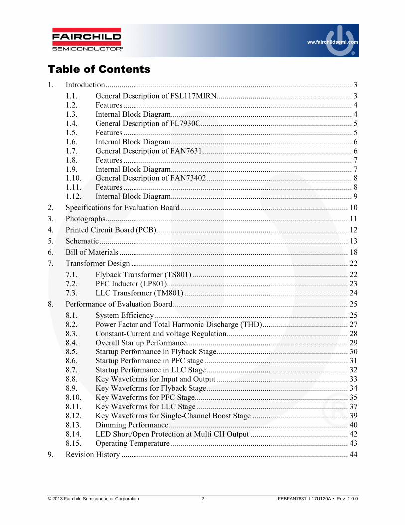
Table of Contents
1. Introduction ............................................................................................................................ 3
1.1. General Description of FSL117MIRN.................................................................... 3
1.2. Features ................................................................................................................... 4
1.3. Internal Block Diagram........................................................................................... 4
1.4. General Description of FL7930C............................................................................ 5
1.5. Features ................................................................................................................... 5
1.6. Internal Block Diagram........................................................................................... 6
1.7. General Description of FAN7631 ........................................................................... 6
1.8. Features ................................................................................................................... 7
1.9. Internal Block Diagram........................................................................................... 7
1.10. General Description of FAN73402 ......................................................................... 8
1.11. Features ................................................................................................................... 8
1.12. Internal Block Diagram........................................................................................... 9
2. Specifications for Evaluation Board .................................................................................... 10
3. Photographs.......................................................................................................................... 11
4. Printed Circuit Board (PCB) ................................................................................................ 12
5. Schematic ............................................................................................................................. 13
6. Bill of Materials ................................................................................................................... 18
7. Transformer Design ............................................................................................................. 22
7.1. Flyback Transformer (TS801) .............................................................................. 22 7.2. PFC Inductor (LP801)........................................................................................... 23
7.3. LLC Transformer (TM801) .................................................................................. 24
8. Performance of Evaluation Board ........................................................................................ 25
8.1. System Efficiency ................................................................................................. 25 8.2. Power Factor and Total Harmonic Discharge (THD) ........................................... 27 8.3. Constant-Current and voltage Regulation ............................................................. 28
8.4. Overall Startup Performance................................................................................. 29 8.5. Startup Performance in Flyback Stage .................................................................. 30 8.6. Startup Performance in PFC stage ........................................................................ 31
8.7. Startup Performance in LLC Stage ....................................................................... 32 8.8. Key Waveforms for Input and Output .................................................................. 33 8.9. Key Waveforms for Flyback Stage ....................................................................... 34 8.10. Key Waveforms for PFC Stage............................................................................. 35
8.11. Key Waveforms for LLC Stage ............................................................................ 37 8.12. Key Waveforms for Single-Channel Boost Stage ................................................ 39 8.13. Dimming Performance .......................................................................................... 40
8.14. LED Short/Open Protection at Multi CH Output ................................................. 42 8.15. Operating Temperature ......................................................................................... 43
9. Revision History .................................................................................................................. 44

© 2013 Fairchild Semiconductor Corporation 3 FEBFAN7631_L17U120A • Rev. 1.0.0
This user guide supports the evaluation kit for the FSL117MRIN, FL7930C, FAN7631,
and FAN73402; orderable as FEB-L017U120B. It should be used in conjunction with the
product datasheets as well as Fairchild’s application notes and technical support team.
Please visit Fairchild’s website at www.fairchildsemi.com.
1. Introduction
This document describes a proposed solution for a 120 W LED driver consisting of an
AC-DC converter for flyback bias regulation, a boost converter for Power-Factor-
Correction (PFC), an LLC resonant converter for a single LED channel with constant
current and voltage or individual boost converters for two LED channels with constant
current and dimming control. The input voltage range is 85 VRMS – 300 VRMS and there
are DC outputs with a constant current of 2.4 A at 50 VMAX for a single LED channel or
with constant current and dimming of 1.2 V at 100 V for two LED channels.
The power supply mainly utilizes:
FSL117MRIN – Green Mode Fairchild Power Switch (FPS™)
FL7930B – CRM PFC Controller
FAN7631 – Half-Bridge LLC Controller
FAN73402 – Single-Channel Boost Controller (for each controller)
FCPF190N60E and FCPF600N60Z – Fairchild SuperFET® Technology
FDPF14N30 – Fairchild UniFET® Technology N-Channel MOSFET
FFPF08H60S – Fairchild Hyperfast Rectifier
MBR20200CT – Fairchild Schottky Rectifier
RURD620CCS9A – Fairchild Ultra-Fast Recovery Rectifier (for discrete)
This document contains important information (e.g. schematic, bill of materials, printed
circuit board layout, transformer design documentation), and the typical operating
characteristics supporting this evaluation board.
1.1. General Description of FSL117MRIN
The FSL117MRIN is an integrated Pulse Width Modulation (PWM) controller and 700 V
SenseFET specifically designed for offline Switched-Mode Power Supplies (SMPS) with
minimal external components. The PWM controller includes an integrated fixed-
frequency oscillator, Line Over-Voltage Protection (LOVP), Under-Voltage Lockout
(UVLO), Leading-Edge Blanking (LEB), optimized gate driver, internal soft-start,
temperature-compensated precise current sources for loop compensation, and self-
protection circuitry. Compared with a discrete MOSFET and PWM controller solution,
the FSL117MRIN can reduce total cost, component count, size, and weight; while
simultaneously increasing efficiency, productivity, and system reliability. This device
provides a basic platform for cost-effective design of a flyback converter.

© 2013 Fairchild Semiconductor Corporation 4 FEBFAN7631_L17U120A • Rev. 1.0.0
1.1.1. Features
Advanced Soft Burst Mode for Low Standby Power and Low Audible Noise
Random Frequency Fluctuation (RFF) for Low Electromagnetic Interference (EMI)
Pulse-by-Pulse Current Limit
Overload Protection (OLP), Over-Voltage Protection (OVP), Abnormal Over-Current
Protection (AOCP), Internal Thermal Shutdown (TSD) with Hysteresis, Output-Short
Protection (OSP), Line Over-Voltage Protection (LOVP), and Under-Voltage
Lockout (UVLO) with Hysteresis
Low Operating Current (0.4 mA) in Burst Mode
Internal Startup Circuit
Internal Avalanche-Rugged 700 V SenseFET
Built-in Soft-Start: 15 ms
Auto-Restart Mode
1.1.2. Internal Block Diagram
tON<tOSP(1.0μs)
OSC
90µA
IFB
R
3R
VCC Good
VSTR Drain
GND
Gate
Driver
VCC
LEB (300ns)
PWM
1
5 2 6,7,8
3
2.0µA
IDELAY S Q
R Q
S Q
R Q
Vburst
0.35V / 0.50V
VAOCP
VOSP
VOVP
24.5V
VCC
LPF
TSD
VSD
7.0V
Soft-Start
7.5V / 12VVCC GoodVREF
FSL1117MRIN
VCC VREF
Random
ICH
Soft Burst
VINH / VINL
VIN
4
FB
Figure 1. Block Diagram of FSL117MRIN

© 2013 Fairchild Semiconductor Corporation 5 FEBFAN7631_L17U120A • Rev. 1.0.0
1.2. General Description of FL7930C
The FL7930C is an active Power Factor Correction (PFC) controller for low- to high-
power lumens applications that operate in Critical Conduction Mode (CRM). It uses a
voltage-mode PWM that compares an internal ramp signal with the error amplifier output
to generate a MOSFET turn-off signal. Because the voltage-mode CRM PFC controller
does not need rectified AC line voltage information, it saves the power loss of an input
voltage-sensing network. FL7930B provides over-voltage, open-feedback, over-current,
input-voltage-absent detection, and under-voltage lockout protections. The FL7930B can
be disabled if the INV pin voltage is lower than 0.45 V and the operating current
decreases to a very low level. Using a new variable on-time control method, Total
Harmonic Discharge (THD) is lower than conventional CRM boost PFC ICs. The
FL7930C provides a PFC Ready pin that can be used to shutdown the boost power stage
when PFC output voltage reaches the proper level (with hysteresis).
1.2.1. Features
Additional PFC-Ready Function
Input-Voltage-Absent-Detection Circuit
Maximum Switching Frequency Limitation.
Internal Soft-Start with Overshoot Prevention
Internal Total harmonic Distortion (THD) Optimizer
Precise Adjustable Output Over-Voltage Protection (OVP)
Open-Feedback Protection and Disable Function
Zero Current Detector (ZDC)
150 μs Internal Startup Timer
MOSFET Over-Current Protection (OCP)
Under-Voltage Lockout with 3.5 V Hysteresis (UVLO)
Low Startup (40 μA) and Operating Current (1.5 mA)
Totem-Pole Output with High State Clamp
+500 / -800 mA Peak Gate Drive Current
SOP-8 Package

© 2013 Fairchild Semiconductor Corporation 6 FEBFAN7631_L17U120A • Rev. 1.0.0
1.2.2. Internal Block Diagram
VCC
ZCD
VTH(ZCD)
VCC
OUT
+
-
S
QR
Q
+
-INV 1
5
COMP 3
clamp circuit
+
-VCS_LIM
40kW
8pF
4 CS
0.450.35
disable
2.6752.5
disable
2.241.60
VBIAS
+
-
VZ
+
-
VTH(S/S)
128.5
VO(MAX)
VCC
2.5VREF
internal bias
VBIAS
VREF
gate
driver
restart timer
7
8
6 GND
+
-
INV_openOVPUVLO
RDY 2
reset
reset
H:open
thermal shutdown
fMAX limit
VREF
Startup
without
Overshoot
VREF stair step
Cla
mp
circu
it
THD optimized
sawtooth
generator
1V
6.5V
VIN-Absent
Detection
VCC
Figure 2. Block Diagram of FL7930C
1.3. General Description of FAN7631
The FAN7631 is a pulse-frequency modulation controller for high-efficiency half-bridge
resonant converters that includes a high-side gate drive circuit, an accurate current-
controlled oscillator, and various protection functions. The FAN7631 features include
variable dead time, high operating frequency up to 600 kHz, protections such as LUVLO,
and a selectable latch or A/R protection using the LS pin for user convenience. The Zero-
Voltage-Switching (ZVS) technique reduces the switching losses and improves the
efficiency significantly. ZVS also reduces the switching noise noticeably, which allows a
small Electromagnetic Interference (EMI) filter. Offering everything necessary to build a
reliable and robust resonant converter, the FAN7631 simplifies designs and improves
productivity and performance. The FAN7631 can be applied to resonant converter
topologies such as series resonant, parallel resonant, and LLC resonant converters.

© 2013 Fairchild Semiconductor Corporation 7 FEBFAN7631_L17U120A • Rev. 1.0.0
1.3.1. Features
Variable Frequency Control with 50% Duty Cycle for Half-bridge Resonant
Converter Topologies
High Efficiency through Zero-Voltage-Switching (ZVS)
Up to 600 kHz Operating Frequency
High Gate-Driving Current +500 mA/-1000 mA
Precise Adjustable Output Over-Voltage Protection (OVP)
Programmable Dead Time using a Resistor
Pulse Skipping and Burst Operation for Frequency Limit (programmable) at Light-
Load Condition
Simple Remote on/off Control with Selectable Latch or A/R using FI or LS pin
Protection Function; Over-Voltage Protection (OVP), Overload Protection (OLP),
Over-Current Protection (OCP), Abnormal Over-Current Protection (AOCP), Internal
Thermal Shutdown (TSD) and High Precise Line Under-Voltage Lockout (LUVLO)
Level-Change OCP Function during Startup.
SOP-16 Package
1.3.2. Internal Block Diagram
HO
LO
HVCC
CTR
12
LVCC
DT
DT
DT
2RT
CON
CS
LVCC < 5VSG
PG
LS
SS
Current Controlled Oscillator
VREF
Internal Bias
< 600kHz
Current
Steering
Block
High-Side
Gate Driver
Low-Side
Gate Driver
HVCC
Good
VFI
50% Duty Cycle
FI
TSD
A/R
Protection
Latch
Protection
+
-
10 / 12.5 V
+
-
VRT
+
-
+
-
+
-
S
R
Q
Q
VTL
S
R
Q
Q
S
R
Q
Q+
-
+
-
VOVP
+
-
0.6 V/ 0.4 V
+
-
+
-
OCP
AOCP
LVcc Good
OVP
OCP
OVP
VRT
3
10
7
18 6
9
11
4
14
15
16
LVcc Good
VSS_ATART
/ VSS_END
Frequency
Divider
+
-
VSS_START
IOLP
ISS2
ISS1
VOCP
VAOCP
OLP
Block
+
-
CS
OLP
8.7 / 9.2 V
-0.56V
-1.1V
CS
4V
SKIP
3V
10µA
LINE Good
ILINE
30µA
30µA
2V
+
-
VSS_END
VTH
ICTC
2ICTC
Figure 3. Block Diagram of FAN7631

© 2013 Fairchild Semiconductor Corporation 8 FEBFAN7631_L17U120A • Rev. 1.0.0
1.4. General Description of FAN73402
The FAN73402 is a single-channel boost controller that integrates an N-channel power
MOSFET for PWM dimming using Fairchild’s proprietary planar Double-diffused
MOSFET (DMOS) technology. The IC operates as a constant-current source for
driving high-current LEDs. It uses Current Mode control with programmable slope
compensation to prevent sub-harmonic oscillation. The IC provides protections
including: open-LED protection, over-voltage protection, and direct-short protection
for high system reliability. The IC internally generates a FAULT signal with delay if an
abnormal LED string condition occurs. PWM dimming and analog dimming functions
can be implemented independently. Internal soft-start prevents inrush current flowing
into output capacitor at startup.
1.4.1. Features
Single-Channel Boost LED Switch
Internal Power MOSFET for PWM Dimming:
RDS(ON)=1.0 Ω at VGS=10 V, BVDSS=200 V
Current-Mode PWM Control
Internal Programmable Slope Compensation
Wide Supply Voltage Range: 10 V to 35 V
LED Current Regulation: ±1%
Programmable Switching Frequency
Analog and PWM Dimming
Wide Dimming Ratio: On Time=10 µs to DC
Cycle-by-Cycle Current Limiting
Thermal Shutdown: 150°C
Open-LED Protection (OLP)
Over-Voltage Protection (OVP)
Over-Current Protection (OCP)
Error Flag Generation (for External Load Switch)
Internal Soft-Start
16-Lead SOIC Package

© 2013 Fairchild Semiconductor Corporation 9 FEBFAN7631_L17U120A • Rev. 1.0.0
1.4.2. Internal Block Diagram
Figure 4. Block Diagram of FAN73402
+
-
+
-R
SQ
Gate
DriverCMP
ADIM
DRV
GND
CS
BDIM
TSD
16 Steps
Internal Soft-Start
1/4gm
OCP
+
-
VCC
5V, max. 3mA
UVLO 9V
Voltage Reference
& Internal Bias
Hys. 1.0V
-
+
Current Sense
Drain
SEN
PWM
PWM
Current
Sense
3VOVP
+
-
OVP 100mV
20μs Delay
ADIM*4
1.4~4V
1μs Delay
BDIM
OLPi
+
-
0.2V
PWM
5μs Delay
PWM
REF
0.3~3V
SlopeCompensation
CLK+LEB
45µA
-
+
0.5V
5k
Switch Off
-
+
BurstOperation
100mV
0.5V
4V
3ms at 200kHz
POR
640µs at 200kHz
Auto-Restart
S
R
Q
Dim off
Dim off
RTOscillator
OLPi
ENA
-
+
1.22V
40.96msat 200kHzDebounce
Time
OLP
OLP
FAULT
Hys. 70mV
End of Soft-Start

© 2013 Fairchild Semiconductor Corporation 10 FEBFAN7631_L17U120A • Rev. 1.0.0
2. Specifications for Evaluation Board
Table 1. Specifications for LED Lighting Lamp
Description Symbol Value Comments
Input Voltage
VIN.MIN 85 VAC Minimum Input Voltage
VIN.MAX 300 VAC Maximum Input Voltage
VIN.NOMINAL 120 V/230 V Nominal Input Voltage
Frequency fIN 60 Hz/50 Hz Line Frequency
Output
Voltage VOUT_SINGLE 50 V Output Voltage for Single Channel LED
VOUT_MULTI. 100 V Output Voltage for Multi Channel LED
Current IOUT_SINGLE 2.4 A Output Current for Single Channel LED
IOUT_MULTI. 1.2 A Output Current for Multi Channel LED
Efficiency [Single Channel]
Eff85VAC 87.77% Efficiency at 85 VAC Line Input Voltage
Eff120VAC 90.06% Efficiency at 120 VAC Line Input Voltage
Eff140VAC 90.86% Efficiency at 140 VAC Line Input Voltage
Eff180VAC 91.55% Efficiency at 180 VAC Line Input Voltage
Eff230VAC 91.99% Efficiency at 230 VAC Line Input Voltage
Eff300VAC 92.33% Efficiency at 300 VAC Line Input Voltage
Standby Power
P85VAC 0.283 W Standby Power at 85 VAC Line Input Voltage
P120VAC 0.306 W Standby Power at 120 VAC Line Input Voltage
P140VAC 0.315 W Standby Power at 140 VAC Line Input Voltage
P180VAC 0.319 W Standby Power at 180 VAC Line Input Voltage
P230VAC 0.341 W Standby Power at 230 VAC Line Input Voltage
P300VAC 0.397 W Standby Power at 300 VAC Line Input Voltage
PF/THD
PF/THD85VAC 0.998/4.58% PF/THD at 85 VAC Line Input Voltage
PF/THD120VAC 0.997/4.65% PF/THD at 120 VAC Line Input Voltage
PF/THD140VAC 0.995/4.74% PF/THD at 140 VAC Line Input Voltage
PF/THD180VAC 0.992/5.32% PF/THD at 180 VAC Line Input Voltage
PF/THD230VAC 0.980/7.89% PF/THD at 230 VAC Line Input Voltage
PF/THD300VAC 0.945/15.13% PF/THD at 300 VAC Line Input Voltage
Temperature
FSL117MRIN TFSL117MRIN 53.9°C FSL117MRIN Temperature at 25°C
FAN73402 TFAN73402 82.1°C FAN73402 Temperature at 25°C
MOSFET
TPFC 63.0°C PFC MOSFET Temperature at 25°C
TLLC 59.2°C LLC MOSFET Temperature at 25°C
TBoost_Channel 61,8°C Boost Channel MOSFET Temperature at 25°C
TLLC 67.5°C LLC Rectifier Temperature at 25°C
TBoost_Channel 69.5°C Boost Channel Rectifier Temperature at 25°C
T_LLC 72.6°C LLC Transformer Temperature at 25°C
All data of the evaluation board measured with the board enclosed in a case and external
temperature around 25°C.

© 2013 Fairchild Semiconductor Corporation 11 FEBFAN7631_L17U120A • Rev. 1.0.0
3. Photographs
Figure 5. Top View [Dimensions: 232mm (L) x 114 mm (W) x 27 mm (H)]
Figure 6. Bottom View [Dimensions: 232mm (L) x 114 mm (W) x 27 mm (H)]

© 2013 Fairchild Semiconductor Corporation 12 FEBFAN7631_L17U120A • Rev. 1.0.0
4. Printed Circuit Board (PCB)
232 mm
114 m
m
Figure 7. Top Pattern
Figure 8. Bottom Pattern
© 2013 Fairchild Semiconductor Corporation 13 FEBFAN7631_L17U120A • Rev. 1.0.0
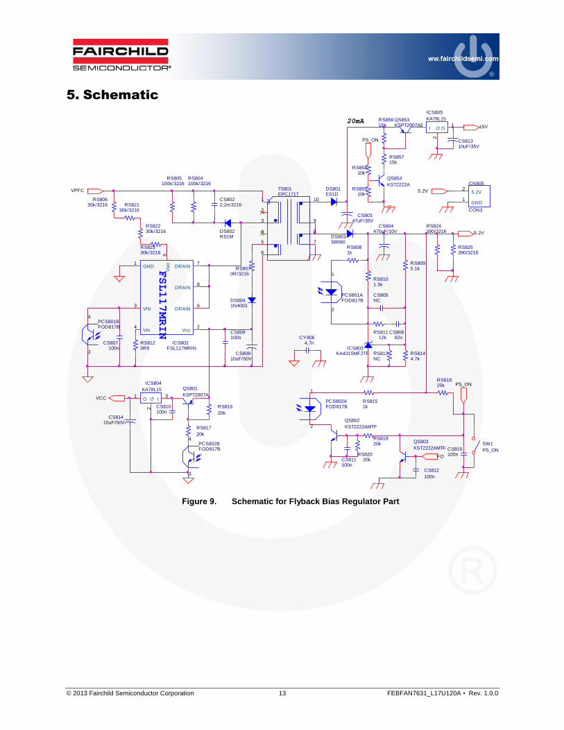
5. Schematic
Figure 9. Schematic for Flyback Bias Regulator Part
PCS802BFOD817B
4
3
ICS805
KA78L15
O1
I3
G2
DS803SB560
CS807100n
RS81112k
CS80682n
CS805NC
CY8064,7n
RS80630k/3216
RS8095.1k
RS813NC
RS8144.7k
ICS802FSL117MRIN
DRAIN8
DRAIN6
GND1
Vstr
5
Vin4
DRAIN7
Vcc2
Vf b3
5.2V
CS804470uF/10VDS802
RS1M
FSL117MRIN
DS801ES1D
CS80347uF/35V
RS804100k/3216
RS8070R/3216
CS80810uF/50V
CS8022.2n/3216
DS8041N4003
CS809100n
PCS801AFOD817B
1
2
PCS801BFOD817B
4
3
RS8120R0 ICS803
KA431SMF2TF
RS805100k/3216
RS8081k
RS8101.5k
TS801EPC1717
1
2
3
4
5
6
7
10
8
9RS824390/3216
CS811100n
RS825390/3216
RS85615k 15V
RS817
20k
5.2V
CN805
CON3
5.2V2
GND1
RS816
20k
PS_ON
RS81920k QS803
KST2222AMTF
CS81310uF/35V
CS810100n
RS85715k
RS85510k
QS854
KST2222A
RS85810k
PS_ON
CS815100n
QS802
KST2222AMTF
RS82020k
RS81820k
RS82130k/3216
QS853KSPT2907A
RS8151k
RS82230k/3216
PCS802AFOD817B
1
2
VPFC
RS82330k/3216
20mA
VCC
CS812
100n
ICS804
KA78L15
O1
I3
G2
SW1
PS_ON
CS81410uF/50V
QS801
KSPT2907A
FO

© 2013 Fairchild Semiconductor Corporation 14 FEBFAN7631_L17U120A • Rev. 1.0.0
Figure 10. Schematic for PFC Part
QP802FCPF190N60E
CP802
330uF/250V
DP803
ES1D
ICP801FL7930C
VCC8
GND6
INV1
ZCD5
CS4
OUT7
READY2
COMP3
RP8044.3M
RP8140.1/5W
RP8094.3M
CP803680n/630V
RP8074.3M
CN801INLET
1 2 3
LX802CV630055
t
RT13D15
VPFC
RX8021M/3216
t
RT23D15
CP801
330uF/250V
RX8031M/3216
FS801250VAC, T6.3AH
RP817NC
LP801PFC3819QM
2
7 6
4
RP811150
PFC OK
RP80510K
DP8011N5408
RP80310
CP80510uF/35V
DP804LL4148
CP806100n
CP8111n
RP801
4.3M
RP80647k
CP8091n
ZNR80110D561K
RP81210k
+-
~ ~
DX801D15XB60
RP8153.3
CX802470nF
CX801470nF
RX8011M/3216
RP813
91K
CY801470p
RP816
4.7K
LX801CV630055
CP8081u
VCC
CP807200n
CY802470p
FL
7930C
ZDP801NC
DP802
FFPF08H60S

© 2013 Fairchild Semiconductor Corporation 15 FEBFAN7631_L17U120A • Rev. 1.0.0
Figure 11. Schematic for LLC Part
※ RM830 should be NC in case of 50 V/2.4 A output and use 16 k value in case of 100 V/1.2 A output.
RM
826
1K
DM
810
ES
1D
RM
825
1K
/3216
PF
C O
K
CM
823
5.6
n
CM
808
470n
RM
839
10k
DM
804
UF
4004
RM
840
2.2
k/F
CM
810
10n
RM
812
3.3
R
CM
814
10p
CM
806
220n
RM
837
10k/F
RM
809
10k
CY
803
4.7
n
RM
822
3.3
R
QM
801
FC
PF
600N
60Z
CM
809
47n
TM
801
SR
X43E
M
1 2 3 4 5
711
10
9 812
VC
C
JP
M801
JU
MP
ER
QM
802
FC
PF
600N
60Z
RM
823
10k
CM
805
NC
DM
808
LL4148
RM
833
18k/3
216
CM
812
10uF
/35V
ICM
801
FA
N7631
LS
8
FI
6
NC
5
DT
4
SG
7
RT
2
SS
3
CS
9
PG
10
LO
11
LV
cc
12
NC
13
CTR
14
HO
15
HV
CC
16
CO
N1
DM
802
MB
R20200C
T
1 32
RM
810
2.7
k/F
RM
840
18k/3
216
DM
807
LL4148
RTN
ISE
N
DM
805
LL4148
CM
824
47n/3
216
RM
806
1.1
K
ISE
N
50V /2.4A
CM
811
100n
VPFC=450V
RM
811
4.7
K
CM
803
680uF
/63V
RM
841
39k
RM
814
5.6
k
RM
817
10/3
216
CM
816
3.9
nF
/630V
ICM
803
TS
M103W
VC
C8
INV
26
OU
T1
1
Non_IN
V2
5V
EE
4
OU
T2
7IN
V1
2
Non_IN
V1_re
f3
CM
820
8.2
nF
RM
836
22k
RM
829
20k
DM
803
LL4148
PC
M801A
FO
D817B
1 2
15V
CM
817
8.2
n
RM
832
5.1
k
RM
828
15k
RM
807
24k/F
RM
802
0.2
/1W
RM
801
0.2
/1W
RM
830
12k
RM
805
1M
DM
801
MB
R20200C
T1 3
2V
LE
D+
RM
808
2.2
M
FAN7631
PC
M801B
FO
D817B
4 3
JP
M802
JU
MP
ER
RM
813
2.2
M
CM
801
680uF
/63V
ISE
N
RM
827
39k
RM
803
27k/F
RM
820
24k
RM
821
100K
DM
809
LL4148
CM
802
680uF
/63V
CM
804
680uF
/63V
CM
807
10n
DM
806
LL4148
RM
838
5.1
k
CM
818
100n
© 2013 Fairchild Semiconductor Corporation 16 FEBFAN7631_L17U120A • Rev. 1.0.0
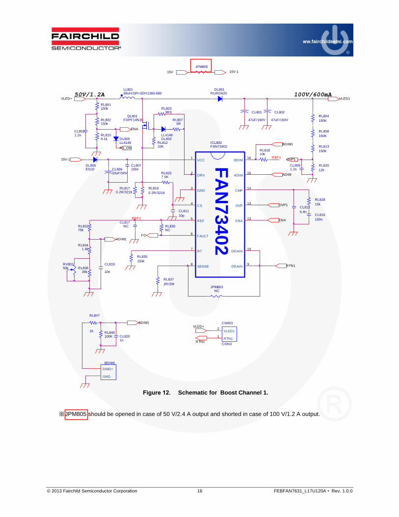
Figure 12. Schematic for Boost Channel 1.
※ JPM805 should be opened in case of 50 V/2.4 A output and shorted in case of 100 V/1.2 A output.
PS_ON
OVP1
DL801RURD620
RTN1
VLED+
RTN1
CN803
CON3
VLED12
RTN11
ADIM
OVP1
CL8031.2n
ENA
RL801150k
RL802150k
RL8109.1k DL803
LL4148
VLED1
RV80150k
JPM805
RL83275k
RL835
150k
RL837
2R/2W
RL8070R
CL819
10n
CL817NC
CL8091.2n
RL81810k
RL830NC
CL812
6.8n
RL828
15k
RL8227.5K
CL815
100n
FA
N7
34
02
FO
REF1
ICL802FAN73402
FAULT6
REF5
SENSE8
DRAIN9
RT7
GND3
CS4
DRV2
DRAIN10
CMP14
ENA12
VCC1
OVP13
BDIM16
ADIM15
LL80168uH/SPI-SDH1360-680
CL80610uF/50V
RL808
150K
15V
QL801FDPF14N30
RL8033R3
CL807100n
RL813
150K
CL801
47uF/160V
RL820
12k
RL816
0.2R/3216
RL804
150K
RL81210K
CL802
47uF/160V
15V-1
15V-1
VLED+
REF1
50V/1.2A
RL8341.8k
RL847
1K RL848100K CL820
1n
BDIM1
ADIM1
BDIM1
ENA
JPM803NC
DL805LL4148
RL83839k
DL806ES1D
BDIM1
DIM1+
GND
CL811
10p
RL8170.2R/3216
100V/600mA

© 2013 Fairchild Semiconductor Corporation 17 FEBFAN7631_L17U120A • Rev. 1.0.0
Figure 13. Schematic for Boost Channel 2
100V/600mA
CL82110uF/50V
OVP2
RL849100K
RL8501K
CL8231n
BDIM2
DL807ES1D
RV80250k
FA
N7
34
02
RL840
2R/2W
RL84175k
CL82210n
ADIM2
BDIM2
DIM2+
GND
OVP2
RTN2
DL804LL4148
VLED2
VLED+
RTN1
CN804
CON3
VLED12
RTN11
RL8391.8k
50V/1.2A
RL84239k
ADIM2
RL8260.2R/3216
RL836
150K
RL8090R
CL818NC
CL8101.2n
RL819
10k
RL831
NC
CL814
6.8n
RL829
15k
RL8237.5K
CL816
100n
FO
REF2
ICL801FAN73402
FAULT6
REF5
SENSE8
DRAIN9
RT7
GND3
CS4
DRV2
DRAIN10
CMP14
ENA12
VCC1
OVP13
BDIM16
ADIM15
LL80268uH/SPI-SDH1360-680
RL811
150k
QL802FDPF14N30
RL8053R3
CL808
0.1u
DL802RURD620
RL815
150k
RL821
12k
CL804
47uF/160V
RL825
0.2R/3216
RL806
150k
RL81410K
CL805
47uF/160V
15V-1
VLED+
ENA
BDIM2
CL813
10p
JPM804NC

© 2013 Fairchild Semiconductor Corporation 18 FEBFAN7631_L17U120A • Rev. 1.0.0
6. Bill of Materials
No. Part Reference Part Value Qty. Description Vendor
1 BDIM1, BDIM2 2 Pin 1 2 Pin Connector Molex
2 CL801, CL802, CL804, CL805 47 µF/160 V 4 Electrolytic Capacitor Samyoung
3 CL803, CL809, CL810 C0805C112J5GACTU 3 1.2 nF/50 V, SMD
MLCC Kemet
4 CL806, CS808, CS814, CL821 KMG 10 µF/35 V 4 Electrolytic Capacitor Samyoung
5
CP806, CS807, CL807, CS809, CS810, CS811, CM811, CS812, CS815, CL815, CL816, CM818, CL808
C0805C104J5GACTU 13 1.2 nF/50 V, SMD
MLCC Kemet
6 CL811, CL813, CM814 C0805C100J5GACTU 3 10 pF/50 V, SMD
MLCC Kemet
7 CL812, CL814 C0805C683J5GACTU 2 6.8 nF/50 V, SMD
MLCC Kemet
8 CM807, CM810, CL819, CL822 C0805C103J5GACTU 4 10 nF/50 V, SMD
MLCC Kemet
9 CP809,CP811,CL820,CL823 C0805C102J5GACTU 4 1 nF/50 V, SMD
MLCC Kemet
10 CM801, CM802, CM803, CM804 NHL 330 µF/250V 4 Electrolytic Capacitor Samyoung
11 CM806 C0805C224J5GACTU 1 220 nF/50 V, SMD
MLCC Kemet
12 CM808 C0805C474J5GACTU 1 470 nF/50 V, SMD
MLCC Kemet
13 CM809 C0805C473J5GACTU 1 47 nF/50 V, SMD
MLCC Kemet
14 CM816 4.7 nF/630 V 1 Film Capacitor Sungho
15 CM817, CM820 C0805C822J5GACTU 2 8.2 nF/50 V, SMD
MLCC Kemet
16 CM823 C0805C562J5GACTU 1 5.6 nF/50 V, SMD
MLCC Kemet
17 CM824 C1206C473J1GACTU 1 47 nF/100 V, SMD
MLCC Kemet
18 CN801 3 Pin 1 3 Pin Connector Molex
19 CN802, CN803, CN804, CN805 2 Pin 4 2 Pin Connector Molex
20 CP801, CP802 KMG 330 µF/250 V 2 Electrolytic Capacitor Samyoung
21 CP803 680 n/630 V 1 Film Capacitor Sungho
22 CP805, CM812, CS813 KMG 10 µF/35 V 3 Electrolytic Capacitor Samyoung
23 CP807 C0805C204J5GACTU 1 200 nF/50 V, SMD
MLCC Kemet
24 CP808 C0805C105J5GACTU 1 1 µF/50 V, SMD
MLCC Kemet
25 CS802 C1206C202J5GACTU 1 2.2 nF/630 V, SMD
MLCC Kemet
26 CS803 KMG 47 µF/35 V 1 Electrolytic Capacitor Samyoung
27 CS804 KMG 470 µF/35 V 1 Electrolytic Capacitor Samyoung

© 2013 Fairchild Semiconductor Corporation 19 FEBFAN7631_L17U120A • Rev. 1.0.0
No. Part Reference Part Value Qty. Description Vendor
28 CS806 C1206C823J5GACTU 1 82 nF/50 V, SMD
MLCC Kemet
29 CX801, CX802 MPX334 2 X-Capacitor Carli
30 CY801, CY802 SDC471J10FS10 2 Y-Capacitor Samwha
31 CY803, CY806 SDC472J10FK7 1 Y-Capacitor Samwha
32 DL801, DL802 RURD620 2 200 V/6 A Ultrafast
Diode Fairchild
Semiconductor
33 DM803, DL803, DP804, DL804, DM805, DL805, DM806, DM807, DM808, DM809
LL4148 10 Small Signal Diode Fairchild
Semiconductor
34 DS801, DP803, DL806, DL807, DM810
ES1D 5 200 V/1 A, Ultra-Fast
Diode Fairchild
Semiconductor
35 DM801, DM802 MBR20200CT 2 200 V/20 A, Schottky
Rectifier Fairchild
Semiconductor
36 DM804 UF4004 1 400 V/1.0 A, Ultra-
Fast Diode Fairchild
Semiconductor
37 DP801 1N5408 1 1000 V/3 A, General
Rectifier Fairchild
Semiconductor
38 DP802 FFPF08H60S 1 8 A, 600 V, Hyper-
Fast Diode Fairchild
Semiconductor
39 DS802 RS1M 1 1000 V/1 A, Ultra-
Fast Diode Fairchild
Semiconductor
40 DS803 SB560 1 60 V/5 A, Schottky
Rectifier Fairchild
Semiconductor
41 DS804 1N4003 1 Ultra-Fast Diode Fairchild
Semiconductor
42 DX801 D15XB60 1 600 V 15 A, Bridge
Diode Shindengen
43 FS801 SS-5-3.15 A 1 250 V/3.15 A, Fuse Bussmann
44 HS1 150 mm 1 Heat Sink [Primary]
45 HS2 50 mm 1 Heat Sink
[Secondary]
46 ICL801, ICL802 FAN73402 2 LED Boost Switch Fairchild
Semiconductor
47 ICM801 FAN7631 1 LLC Controller Fairchild
Semiconductor
48 ICM803 TSM103W 1 Dual OP-Amp ST
49 ICP801 FL7930C 1 PFC Controller Fairchild
Semiconductor
50 ICS802 FSL117MRIN 1 Green Mode FPS Fairchild
Semiconductor
51 ICS803 KA431SMF2TF 1 Shunt Regulator Fairchild
Semiconductor
52 ICS804, ICS805 KA78L15 2 15 V Voltage
Regulator Fairchild
Semiconductor
53 JPM805 JUMPER 1 Jumper Molex
54 LL801, LL802 68 µH/SPI-SDH1360-680 2 68 µH, SMD Inductor TDK

© 2013 Fairchild Semiconductor Corporation 20 FEBFAN7631_L17U120A • Rev. 1.0.0
No. Part Reference Part Value Qty. Description Vendor
55 LP801 PFC3819QM 1 300 µH, PFC
Inductor TDK
56 LX801, LX802 CV630055 2 Line Filter TNC
57 PCM801, PCS801, PCS802 FOD817B 3 Opto-Coupler Fairchild
Semiconductor
58 QL801, QL802 FDPF14N30 2 300 V/14 A MOSFET Fairchild
Semiconductor
59 QM801, QM802 FCPF600N60Z 2 600 V/RDSON:0.19 Ω,
MOSFET Fairchild
Semiconductor
60 QP802 FCPF190N60E 1 600 V/RDSON:0.6 Ω,
MOSFET Fairchild
Semiconductor
61 QS801, QS853 KSPT2907A 2 PNP Transistor Fairchild
Semiconductor
62 QS802, QS803, QS854 KST2222AMTF 3 NPN Transistor Fairchild
Semiconductor
63 RL801, RL802, RL804, RL806, RL808, RL811, RL815, RL835, RL836, RL813
RC0805JR-07150KL 10 150 kΩ, 2012 SMD Yageo
64 RL803, RL805 RC0805JR-073R3L 2 3.3 Ω, 2012 SMD Yageo
65 RL807, RL809, JPM801, JPM802, RS812
RC0805JR-070RL 5 0 Ω, 2012 SMD Yageo
66 RL810 RC0805JR-079k1L 1 9.1 kΩ, 2012 SMD Yageo
67 RP805, RM809, RP812, RL812, RL814, RL818, RL819, RM823, RM839, RS855, RS858
RC0805JR-0710kL 11 10 kΩ, 2012 SMD Yageo
68 RL816, RL817, RL825, RL826 RC1206JR-070R2L 4 0.2 Ω, 3216 SMD Yageo
69 RS811, RL820, RL821, RM830 RC0805JR-0712kL 4 12 kΩ, 2012 SMD Yageo
70 RL822 RL823 RC0805JR-077k5L 2 7.5 kΩ, 2012 SMD Yageo
71 RM828, RL828, RL829, RS856, RS857
RC0805JR-0715kL 5 15 kΩ, 2012 SMD Yageo
72 RL832, RL841 RC0805JR-0775kL 2 75 kΩ, 2012 SMD Yageo
73 RL834, RL839 RC0805JR-071k8L 2 1.8 kΩ, 2012 SMD Yageo
74 RL837, RL840 2 Ω/2 W 2 2 Ω, 2 W Resistor Abel
75 RM827, RL838, RM841, RL842 RC0805JR-0739kL 4 39 kΩ, 2012 SMD Yageo
76 RS808, RS815, RM826, RL847, RL850
RC0805JR-071kL 5 1 kΩ, 2012 SMD Yageo
77 RM821, RL848, RL849 RC0805JR-07100kL 3 100 kΩ, 2012 SMD Yageo
78 RM801, RM802 0.2 Ω/1 W 2 0.2 Ω, 1 W Resistor Abel
79 RM803 RC0805FR-0727kL 1 27 kΩ/F, 2012 SMD Yageo
80 RM805 RC0805JR-071ML 1 1 MΩ, 2012 SMD Yageo
81 RM806 RC0805JR-071k1L 1 1.1 kΩ, 2012 SMD Yageo
82 RM807 RC0805FR-0724kL 1 24 kΩ/F, 2012 SMD Yageo
83 RM808, RM813 RC0805JR-072M2L 2 2.2MΩ, 2012 SMD Yageo
84 RM810 RC0805FR-072k7L 1 2.7 kΩ/F, 2012 SMD Yageo
85 RM811, RS814 RC0805JR-074k7L 2 4.7 kΩ, 2012 SMD Yageo
86 RM812, RM822, RP815 RC0805JR-073R3L 3 3.3 Ω, 2012 SMD Yageo
87 RM814 RC0805JR-075k6L 1 5.6 kΩ, 2012 SMD Yageo

© 2013 Fairchild Semiconductor Corporation 21 FEBFAN7631_L17U120A • Rev. 1.0.0
No. Part Reference Part Value Qty. Description Vendor
88 RM817 RC1206JR-0710RL 1 10 Ω, 2012 SMD Yageo
89 RM820 RC0805JR-0724kL 1 24 kΩ, 2012 SMD Yageo
90 RM825 RC1206JR-071KL 1 1 kΩ, 3216 SMD Yageo
91 RS816, RS817, RS818, RS819, RS820, RM829
RC0805JR-0720kL 6 20 kΩ, 2012 SMD Yageo
92 RS809, RM832, RM838 RC0805JR-075k1L 3 5.1 kΩ, 2012 SMD Yageo
93 RM833, RM840 RC1206JR-0718KL 2 18 kΩ, 2012 SMD Yageo
94 RM836 RC0805JR-072k2L 1 2.2 kΩ, 2012 SMD Yageo
95 RM837 RC0805FR-0710kL 1 10 kΩ/F, 2012 SMD Yageo
96 RM840 RC0805FR-072k2L 1 2.2 kΩ/F, 2012 SMD Yageo
97 RP801, RP804, RP807, RP809 RC0805JR-074M3L 4 4.3 MΩ, 2012 SMD Yageo
98 RP803 RC0805JR-0710RL 1 10 Ω, 2012 SMD Yageo
99 RP806 RC0805JR-0747KL 1 47 kΩ, 2012 SMD Yageo
100 RP811 RC0805JR-07150L 1 150 Ω, 2012 SMD Yageo
101 RP813 RC0805JR-0791KL 1 91 kΩ, 2012 SMD Yageo
102 RP814 0.1 Ω/5 W 1 0.1 Ω, 5 W Resistor Abel
103 RP816 RC0805JR-074K7L 1 4.7 kΩ, 2012 SMD Yageo
104 RS804, RS805 RC1206JR-07100KL 2 100 kΩ, 3216 SMD Yageo
105 RS806, RS821, RS822, RS823 RC1206JR-0730KL 4 30 kΩ, 3216 SMD Yageo
106 RS807 RC1206JR-070RL 1 0 Ω, 3216 SMD Yageo
107 RS810 RC0805JR-071k5L 1 1.5 kΩ, 2012 SMD Yageo
108 RS824, RS835 RC1206JR-07120L 1 390 Ω, 3216 SMD Yageo
109 RT1, RT2 3D15 2 NTC Thermistor Daekwang S
110 RV801, RV802 50 kΩ/0.5 W 2 50 kΩ, Variable
Resistor Vishay
111 RX801, RX802, RX803 RC1206JR-071ML 3 1 MΩ, 3216 SMD Yageo
112 SW1 Toggle Switch 1 3 Terminal Switch Phonix
113 TM801 SRX43EM 1 LLC Transformer TDK
114 TS801 EPC1717 1 LLC Transformer TDK
115 ZNR801 10D561K 1 MOV Samwha
116 CL817, CL818, CM805, CS805 NC 4
117 RS813, RP817, JPM803, JPM804, RL830, RL831
NC 6
118 ZDP801 NC 1

© 2013 Fairchild Semiconductor Corporation 22 FEBFAN7631_L17U120A • Rev. 1.0.0
7. Transformer Design
7.1. Flyback Transformer (TS801)
Core: EPC1717 (TDK)
Bobbin: 10 Pin
ECP1717
NP1(5 à6)
NS1 (1 à2)
NS2(3 à4)
NP2(6 à7)
NP1(10à9)
5
6
2
1
NP1
NP2
7
NA
10
9
3
4
NS1
NS2
2mm
Barrier
2mm
Barrier
Figure 14. Transformer Pin Assignment and Configuration
Table 2. Winding Specifications
No. Winding Pin (S → F) Wire Turns Winding Method
1 NP1 5 à 6 0.15φ 100 Ts Solenoid Winding
2 Insulation: Polyester Tape t = 0.025 mm, 3-Layer
3 NS1 1 à 2 0.45φ 12 Ts Solenoid Winding
4 Insulation: Polyester Tape t = 0.025 mm, 3-Layer
5 NP2 6 à 7 0.25φ 44 Ts Solenoid Winding
6 Insulation: Polyester Tape t = 0.025 mm, 3-Layer
7 NA 10 à 9 0.15φ 37 Ts Solenoid Winding
8 Insulation: Polyester Tape t = 0.025 mm, 3-Layer
9 NS2 3 à 4 0.25φ 22 Ts Solenoid Winding
10 Insulation: Polyester Tape t = 0.025 mm, 3-Layer
Table 3. Electrical Characteristics
Pin Specifications Remark
Inductance [Lp] 5 – 7 900 µH ±10% 60 kHz, 1 V
Leakage [Ll] 5 – 7 55 µH 60 kHz, 1 V at Short All Output Pins

© 2013 Fairchild Semiconductor Corporation 23 FEBFAN7631_L17U120A • Rev. 1.0.0
7.2. PFC Inductor (LP801)
Core: PFC3819QM(TDK)
Bobbin: PQM3819, 8 Pin
NS(7à6)
NP (1 à3)
PFC3819QM
8
7
6
5
4
1
2
3
NP
NA
Figure 15. Transformer Pin Assignment and Configuration
Table 4. Winding Specifications
No. Winding Pin (S → F) Wire Turns Winding Method
1 NP 1 à 3 0.1*65[Litz] 40 Ts Solenoid Winding
2 Insulation: Polyester Tape t = 0.025 mm, 3-Layer
3 NS1 7 à 6 0.45φ 4 Ts Solenoid Winding
4 Insulation: Polyester Tape t = 0.025 mm, 3-Layer
Table 5. Electrical Characteristics
Pin Specifications Remark
Inductance 1 – 3 300 µH ±10% 60 kHz, 1 V

© 2013 Fairchild Semiconductor Corporation 24 FEBFAN7631_L17U120A • Rev. 1.0.0
7.3. LLC Transformer (TM801)
Core: SRX43EM (TDK)
Bobbin: EEX4333P12-1, 12 Pin
SRX43EM
7
9
2
4 NS2
12
NP 10
NS1
NS1(10à7)
NP (4à2) NS2(12à9)
Figure 16. Transformer Pin Assignment and Configuration
Table 6. Winding Specifications
No. Winding Pin (S → F) Wire Turns Winding Method
1 NP 4 à 2 0.1φ * 60 [Litz]] 37 Ts Solenoid Winding
2 Insulation: Polyester Tape t = 0.025 mm, 3-Layer
3 NS1 12 à9
0.08 φ *120[Litz]] 7 Ts Solenoid Winding
NS2 10 à 7 7 Ts Solenoid Winding
4 Insulation: Polyester Tape t = 0.025 mm, 3-Layer
Table 7. Electrical Characteristics
Pin Specifications Remark
Inductance [Lp] 4 – 2 810 µH ±10% 100 kHz, 1 V
Leakage [Lr] 5 – 7 105 µH Short One of the Secondary Windings

© 2013 Fairchild Semiconductor Corporation 25 FEBFAN7631_L17U120A • Rev. 1.0.0
8. Performance of Evaluation Board
Table 8. Test Condition & Equipments
Ambient Temperature TA = 25°C
Test Equipment
AC Power Source: PCR500L by Kikusui
Power Analyzer: PZ4000000 by Yokogawa
Electronic Load: PLZ303WH by KIKUSUI
Multi Meter: 2002 by KEITHLEY, 45 by FLUKE
Oscilloscope: 104Xi by LeCroy
Thermometer: Thermal CAM SC640 by FLIR SYSTEMS
LED: EHP-AX08EL/GT01H-P03 (3W) by Everlight
8.1. System Efficiency
System efficiency is measured in 85 ~ 140 VAC [low line, 60 Hz] and 180 ~ 300 VAC
[high line, 50 Hz] input voltage ranges. The results are for PFC and LLC converters in
which a single LED channel can be connected and measured in the rated load condition
[50 V/2.5 A] 30 minutes after AC power is turned on.
Figure 17. System Efficiency
Table 9. System Efficiency
Input Voltage Output
Voltage[V] Output
Current [A] Input
Power [W] Output
Power [W] Efficiency
85 VAC [60 Hz] 49.69 2.503 141.70 124.37 87.77%
120 VAC [60 Hz] 49.69 2.503 138.10 124.37 90.06%
140 VAC [60 Hz] 49.69 2.507 137.10 124.57 90.86%
180 VAC [50 Hz] 49.69 2.502 135.80 124.32 91.55%
230 VAC [50 Hz] 49.69 2.503 135.20 124.37 91.99%
300 VAC [50 Hz] 49.69 2.501 134.60 124.27 92.33%

© 2013 Fairchild Semiconductor Corporation 26 FEBFAN7631_L17U120A • Rev. 1.0.0
System efficiency is measured in 85 ~ 140 VAC [low line, 60 Hz] and 180 ~ 300 VAC
[high line, 50Hz] input voltage ranges. The results are for PFC and LLC converters in
which a single LED channel can be connected and measured in the 50% load condition
[50 V/1.25 A] 30 minutes after AC power is turned on.
Figure 18. System Efficiency
Table 10. System Efficiency
Input Voltage Output
Voltage[V] Output
Current [A] Output
Voltage [V] Output
Power [W] Efficiency
85 VAC [60 Hz] 49.71 1.252 70.80 62.24 87.91%
120 VAC [60 Hz] 49.71 1.253 69.80 62.29 89.24%
140 VAC [60 Hz] 49.71 1.253 69.60 62.29 89.49%
180 VAC [50 Hz] 49.71 1.254 69.50 62.34 89.69%
230 VAC [50 Hz] 49.71 1.254 69.30 62.34 89.95%
300 VAC [50 Hz] 49.71 1.252 69.10 62.24 90.07%
Table 11 shows stand-by power consumption of 85 VAC~ 140 VAC [low line, 60 Hz] and
180 ~ 300 VAC [high line, 50 Hz] input voltage ranges. The results are measured when the
PS-ON switch is turned off.
Table 11. System Efficiency
Input Voltage Input Power [W]
85 VAC [60 Hz] 0.283
120 VAC [60 Hz] 0.306
140 VAC [60 Hz] 0.315
180 VAC [50 Hz] 0.319
230 VAC [50 Hz] 0.341
300 VAC [50 Hz] 0.397

© 2013 Fairchild Semiconductor Corporation 27 FEBFAN7631_L17U120A • Rev. 1.0.0
8.2. Power Factor and Total Harmonic Discharge (THD)
Power factor and THD were measured in 85 ~ 140 VAC [low line, 60 Hz] and 180 ~
300 VAC [high line, 50 Hz] input voltage ranges. The measured data were results for the
overall system with two channel LED loads connected.
Figure 19. Power Factor & Total Harmonic Distortion
Table 12. Power Factor & Total Harmonic Distortion
Input Voltage Output Current Output Voltage Power Factor THD
85 VAC [60 Hz] 2.503 A 49.69 V 0.998 4.58%
120 VAC [60 Hz] 2.503 A 49.69 V 0.997 4.65%
140 VAC [60 Hz] 2.507 A 49.69 V 0.995 4.74%
180 VAC [50 Hz] 2.502 A 49.69 V 0.992 5.32%
230 VAC [50 Hz] 2.503 A 49.69 V 0.980 7.89%
300 VAC [50 Hz] 2.501 A 49.69 V 0.945 15.13%

© 2013 Fairchild Semiconductor Corporation 28 FEBFAN7631_L17U120A • Rev. 1.0.0
8.3. Constant-Current and Voltage Regulation
Table 13 and Figure 20 show the typical CC/CV performance on the board; showing very
stable CC performance over a wide input range. The results are for PFC and LLC
converters with a single LED channel connected and measured with E-Load [CR Mode].
Table 13. Constant-Current Regulation by Output Voltage Change (25 V~ 50 V)
Input Voltage Min. Max.
CV CC VOUT [V] IOUT [mA] VOUT [V] IOUT [mA]
85 VAC / 60 Hz 49.60 2552 49.70 2560 ±0.03% ±0.04%
120 VAC / 60 Hz 49.60 2552 49.70 2560 ±0.03% ±0.04%
230 VAC / 50 Hz 49.70 2552 49.90 2560 ±0.05% ±0.04%
300 VAC / 50 Hz 49.70 2552 49.90 2560 ±0.05% ±0.04%
Figure 20. Constant-Current Regulation, Measured by E-Load [CR Mode]
© 2013 Fairchild Semiconductor Corporation 29 FEBFAN7631_L17U120A • Rev. 1.0.0
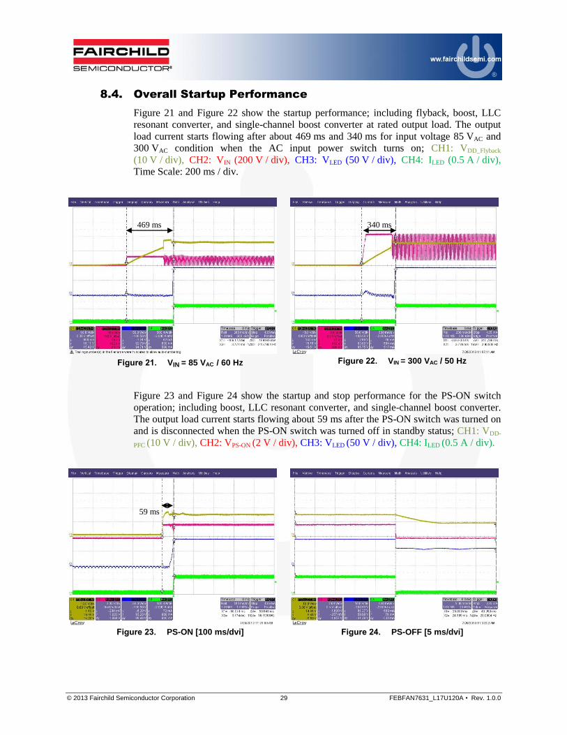
8.4. Overall Startup Performance
Figure 21 and Figure 22 show the startup performance; including flyback, boost, LLC
resonant converter, and single-channel boost converter at rated output load. The output
load current starts flowing after about 469 ms and 340 ms for input voltage 85 VAC and
300 VAC condition when the AC input power switch turns on; CH1: VDD_Flyback
(10 V / div), CH2: VIN (200 V / div), CH3: VLED (50 V / div), CH4: ILED (0.5 A / div),
Time Scale: 200 ms / div.
Figure 21. VIN = 85 VAC / 60 Hz Figure 22. VIN = 300 VAC / 50 Hz
Figure 23 and Figure 24 show the startup and stop performance for the PS-ON switch
operation; including boost, LLC resonant converter, and single-channel boost converter.
The output load current starts flowing about 59 ms after the PS-ON switch was turned on
and is disconnected when the PS-ON switch was turned off in standby status; CH1: VDD-
PFC (10 V / div), CH2: VPS-ON (2 V / div), CH3: VLED (50 V / div), CH4: ILED (0.5 A / div).
Figure 23. PS-ON [100 ms/dvi] Figure 24. PS-OFF [5 ms/dvi]
469 ms 340 ms
59 ms

© 2013 Fairchild Semiconductor Corporation 30 FEBFAN7631_L17U120A • Rev. 1.0.0
8.5. Startup Performance in Flyback Stage
Figure 25 and Figure 26 show the startup performance of the flyback converter. The
output voltage is raised after about 395 ms and 297 ms at 85 VAC and 300 VAC input
voltage, respectively, when the AC input power switch turns on; CH1: VDD-FLYBACK
(10 V / div), CH2: VIN (200 V / div), CH3: V5V (2 V / div), CH4: VDD- FAN73402 (10 V /
div), Time Scale: 200 ms / div.
Figure 25. VIN = 85 VAC / 60 Hz Figure 26. VIN = 300 VAC / 50 Hz
Figure 27 and Figure 28 show the startup and stop performance for the flyback converter
according to PS-ON switch operation. Each output voltage is raised at the same time
when the PS-ON switch is turned on and VDD-FAN73402 drops under UVLO after 100 ms
since PS-ON switch was turned off in standby status; CH1: VDD-PFC (10 V / div), CH2:
VPS-ON (2 V / div), CH3: V5V (2 V / div), CH4: VDD-FAN73402 (10 V / div), Time Scale:
200 ms / div.
Figure 27. PS-ON Figure 28. PS-OFF
395 ms 297 ms

© 2013 Fairchild Semiconductor Corporation 31 FEBFAN7631_L17U120A • Rev. 1.0.0
8.6. Startup Performance in PFC Stage
Figure 29 and Figure 30 show the startup performance; including flyback and boost
converter at the rated output load. The PFC output voltage is raised after about 429 ms
and 339 ms, respectively, for input voltage 85 VAC and 300 VAC condition when the AC
input power switch turns on; CH1: VDD-FLYBACK (10 V / div), CH2: VIN (200 V / div),
CH3: VOUT_PFC (200 V / div), CH4: VRDY (2 V / div), Time Scale: 200 ms / div.
Figure 29. VIN = 85 VAC / 60 Hz Figure 30. VIN = 300VAC / 50 Hz
Figure 31and Figure 32 show the startup and stop performance for the boost converter
according to PS-ON switch operation at rated output load. The PFC output voltage is
raised rapidly when the PS-ON switch is turned on and VDD-PFC drops below UVLO and
PFC output starts discharging PFC output capacitors when PS-ON switch was turned off
in standby status; CH1: VDD-PFC (10 V / div), CH2: VPS-ON (2 V / div), CH3: VOUT-PFC
(200 V / div), CH4: VRDY (2 V / div).
Figure 31. PS-ON, [200 ms/div] Figure 32. PS-OFF, [500 ms/div]
429 ms 339 ms

© 2013 Fairchild Semiconductor Corporation 32 FEBFAN7631_L17U120A • Rev. 1.0.0
8.7. Startup Performance in LLC Stage
Figure 33 and Figure 34 show the startup performance; including flyback, boost, and
LLC converter. The LLC output voltage is raised after about 455 ms and 337 ms,
respectively, for input voltage 85 VAC and 300 VAC condition when the AC input power
switch turns on; CH1: VDD-FLYBACK (10 V / div), CH2: VIN (200 V / div), CH3: VOUT-LLC
(20 V / div), CH4: IOUT-LLC (2 A / div), Time Scale: 200 ms / div.
Figure 33. VIN = 85 VAC / 60 Hz Figure 34. VIN = 300 VAC / 50 Hz
Figure 35 and Figure 36 show the startup and stop performance for the LLC converter
according to the PS-ON switch operation at rated output load. The LLC output current is
raised up to the rated voltage within 50 ms after the PS-ON switch is turned on and the
output current drops to zero quickly when the PS-ON switch is turned off in standby
status; CH1: VDD-LLC (10 V / div), CH2: VPS-ON (2 V / div), CH3: VOUT_LLC (20 V / div),
CH4: IOUT_LLC (2 A / div), Time Scale: 200 ms / div.
Figure 35. PS-ON Figure 36. PS-OFF
455 ms 337 ms

© 2013 Fairchild Semiconductor Corporation 33 FEBFAN7631_L17U120A • Rev. 1.0.0
8.8. Key Waveforms for Input and Output
Figure 37 and Figure 38 show AC input and output waveforms at 85 VAC and 300 VAC
line voltage and rated output load condition, respectively; CH1: IIN (5 A / div), CH2: VIN
(200 V / div), CH3: VLED (50 V / div), CH4: ILED (0.5 A / div), Time Scale: 5 ms / div.
Figure 37. VIN = 85 VAC / 60 Hz, 100% Dim Figure 38. VIN = 300 VAC / 50 Hz, 100% Dim
Figure 39 and Figure 40 show AC input and output waveforms at 85 VAC and 300 VAC
line voltage and 50% output load condition, respectively; CH1: VIN (2 A / div), CH2: VIN
(200 V / div), CH3: VOUT (50 V / div), CH4: ILED (0.5 A / div), Time Scale: 5 ms / div.
Figure 39. VIN = 85 VAC / 60 Hz, 50% Dim Figure 40. VIN = 300 VAC / 50 Hz, 50% Dim

© 2013 Fairchild Semiconductor Corporation 34 FEBFAN7631_L17U120A • Rev. 1.0.0
Figure 41 and Figure 42 show AC input and output waveforms at 85 VAC and 300 VAC
line voltage and 10% output load condition, respectively; CH1: VIN (1 A / div), CH2: VIN
(200 V / div), CH3: VOUT (50 V / div), CH4: ILED (0.5 A / div), Time Scale: 5 ms / div. In
case of 300 VAC, PFC was operated in Burst Mode, so switching pulse were skipped.
Figure 41. VIN = 85 VAC / 60 Hz, 10% Dim Figure 42. VIN = 300 VAC / 50 Hz, 10% Dim
8.9. Key Waveforms for Flyback Stage
Figure 43 and Figure 44 show key waveforms of the flyback stage according to the PS-
ON switch operation at rated output load condition; CH1: IDS- ICS802 (0.5 A / div), CH2:
VDS-ICS802 (200 V / div), CH3: VPS-ON (2 V / div). Time Scale: 200 ms / div.
Figure 43. PS-ON Figure 44. PS-OFF
53 kHz

© 2013 Fairchild Semiconductor Corporation 35 FEBFAN7631_L17U120A • Rev. 1.0.0
8.10. Key Waveforms for PFC Stage
Figure 45 and Figure 46 show key waveforms of PFC stage at 85 VAC line voltage and
rated output load condition; CH1: IDS-QP802 (2 A / div), CH2: VDS-QP802 (200 V / div), CH3:
VAK-DP802 (200 V / div), CH4: IAK-DP802 (2 A / div).
Figure 45. VIN = 85 VAC / 60 Hz, [5 ms/div] Figure 46. VIN = 85 VAC / 60 Hz, [5 µs/div]
Figure 47 and Figure 48 show key waveforms of PFC stage at 85 VAC line voltage and
no-load condition; CH1: IDS_QP802 (0.5 A / div), CH2: VDS_QP802 (200 V / div), CH3:
VAK_DP802 (200 V / div), CH4: IAK_DP802 (0.5 A / div).
Figure 47. VIN = 85 VAC / 60 Hz, [5 ms/div] Figure 48. VIN = 85 VAC / 60 Hz, [2 µs/div]
53 kHz
179 kHz

© 2013 Fairchild Semiconductor Corporation 36 FEBFAN7631_L17U120A • Rev. 1.0.0
Figure 49 and Figure 50 show key waveforms of the PFC stage at 300 VAC line voltage
and rated output load condition; CH1: IDS_QP802 (2 A / div), CH2: VDS_QP802 (200 V / div),
CH3: VAK_DP802 (200 V / div), CH4: IAK_DP802 (2 A / div).
Figure 49. VIN = 300 VAC / 50 Hz, [2 ms/div] Figure 50. VIN = 300 VAC / 50 Hz, [5 µs/div]
Figure 51 and Figure 52 show key waveforms of the PFC stage at 300 VAC line voltage
and no-load condition; CH1: IDS_QP802 (0.5 A / div), CH2: VDS_QP802 (200 V / div), CH3:
VAK_DP802 (200 V / div), CH4: IAK_DP802 (0.5 A / div).
Figure 51. VIN = 300 VAC / 50 Hz, [5 ms/div] Figure 52. VIN = 300 VAC / 50 Hz, [2 µs/div]
62 kHz
Burst

© 2013 Fairchild Semiconductor Corporation 37 FEBFAN7631_L17U120A • Rev. 1.0.0
8.11. Key Waveforms for LLC Stage
Figure 53 and Figure 54 show key waveforms in the primary side of the LLC converter at
rated output load condition; CH1: VGATE-QM802 (10 V / div), CH2: VGATE-QM801 (10 V / div),
CH3: VCr-CM816 (200 V / div), CH4: ILr-TM801 (1.0 A / div).
Figure 53. Rated Load [5 ms/div] Figure 54. Rated Load [2 µs/div]
Figure 55 and Figure 56 show key waveforms in the secondary side of the LLC converter
at rated output load condition; CH1: I_Secondary (2.0 A / div), CH2: VAK_DM802 (100 V / div),
CH3: VAK_DM802 (100 V / div).
Figure 55. Rated Load [5 ms/div] Figure 56. Rated Load [2 µs/div]
212 kHz
© 2013 Fairchild Semiconductor Corporation 38 FEBFAN7631_L17U120A • Rev. 1.0.0
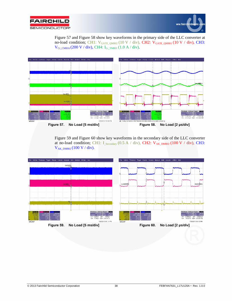
Figure 57 and Figure 58 show key waveforms in the primary side of the LLC converter at
no-load condition; CH1: VGATE_QM802 (10 V / div), CH2: VGATE_QM801 (10 V / div), CH3:
VCr_CM816 (200 V / div), CH4: ILr_TM801 (1.0 A / div).
Figure 57. No Load [5 ms/div] Figure 58. No Load [2 µs/div]
Figure 59 and Figure 60 show key waveforms in the secondary side of the LLC converter
at no-load condition; CH1: I_Secondary (0.5 A / div), CH2: VAK_DM802 (100 V / div), CH3:
VAK_DM802 (100 V / div).
Figure 59. No Load [5 ms/div] Figure 60. No Load [2 µs/div]

© 2013 Fairchild Semiconductor Corporation 39 FEBFAN7631_L17U120A • Rev. 1.0.0
8.12. Key Waveforms for Single-Channel Boost Stage
Figure 61 and Figure 62 show key waveforms of a single-channel boost converter at rated
output load condition; CH1: IDS_QL802 (2.0 A / div), CH2: VDS_QL802 (100 V / div), CH3:
VAK_DL802 (100V / div), CH4: IAK_DL802 (2.0 A / div).
Figure 61. Rated Load [2 ms/div] Figure 62. Rated Load [2 us/div]
Figure 63 and Figure 64 show key waveforms of a single-channel boost converter at 10%
load condition; CH1: IDS_QL802 (2.0 A / div), CH2: VDS_QL802 (100 V / div), CH3: VAK_DL802
(100 V / div), CH4: IAK_DL802 (2.0 A / div).
Figure 63. 10% Load [2 ms/div] Figure 64. 10% Load [2 µs/div]
133 kHz
132 kHz

© 2013 Fairchild Semiconductor Corporation 40 FEBFAN7631_L17U120A • Rev. 1.0.0
8.13. Dimming Performance
Figure 65 and Figure 66 show key waveforms for analog dimming performance of a
single-channel boost converter at 10% ADIM (VADIM: 0.12 V) and 100% BDIM; CH1:
ILED (0.2 A / div), CH2: VGATE-QL802 (5.0 V / div), CH3: VBDIM (5.0 V / div), CH4: VADIM
(0.5 V / div).
Figure 65. 10% ADIM [2 ms/div] Figure 66. 10% ADIM [2 µs/div]
Figure 67 and Figure 68 show key waveforms for PWM dimming performance of a
single-channel boost converter at 100% ADIM (VADIM: 1.2 V) and 1% BDIM; CH1: ILED
(0.5 A / div), CH2: VGATE-QL802 (5.0 V / div), CH3: VBDIM (5.0 V / div), CH4: VADIM
(0.5 V / div).
Figure 67. 1% BDIM [2 ms/div] Figure 68. 1% BDIM [10 µs/div]
200 Hz
© 2013 Fairchild Semiconductor Corporation 41 FEBFAN7631_L17U120A • Rev. 1.0.0
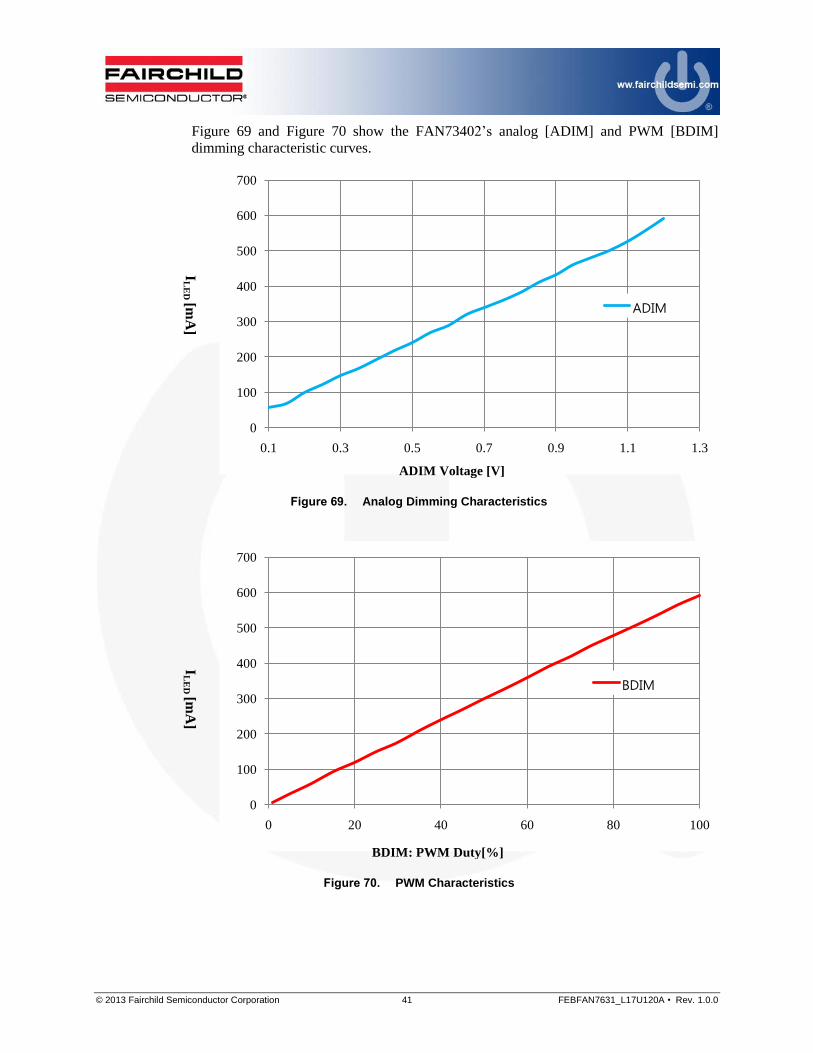
Figure 69 and Figure 70 show the FAN73402’s analog [ADIM] and PWM [BDIM]
dimming characteristic curves.
Figure 69. Analog Dimming Characteristics
Figure 70. PWM Characteristics
0
100
200
300
400
500
600
700
0.1 0.3 0.5 0.7 0.9 1.1 1.3
ADIM
0
100
200
300
400
500
600
700
0 20 40 60 80 100
BDIM
ADIM Voltage [V]
IL
ED
[mA
]
BDIM: PWM Duty[%]
IL
ED
[mA
]

© 2013 Fairchild Semiconductor Corporation 42 FEBFAN7631_L17U120A • Rev. 1.0.0
8.14. LED Short / Open Protection at Multi-Channel Output
Figure 71 and Figure 72 show waveforms for output voltage and current when an LED is
shorted and recovered in one of the LED channels [100 V/0.6 A]; CH1: ILED (0.5 A / div),
CH2: VLED (50 V / div), CH3: VGATE-QL802 (5 V / div), Time Scale: 100 ms / div.
Figure 71. LED Short Figure 72. Recover from LED Short
Figure 73 and Figure 74 show waveforms for output voltage and current when an LED is
opened and recovered in one of the LED channels [100 V/0.6 A]; CH1: ILED (0.5 A / div),
CH2: VLED (50 V / div), CH3: VGATE-QL802 (5 V / div), Time Scale: 100 ms / div.
Figure 73. LED Open Figure 74. Recover from LED Open
LED Open
LED Short

© 2013 Fairchild Semiconductor Corporation 43 FEBFAN7631_L17U120A • Rev. 1.0.0
8.15. Operating Temperature
Figure 75 shows temperatures measured for the primary and secondary active
components in the top side at 85 VAC line voltage and rated output load [two LED
channels: 100 V/1.2 A].
Figure 75. Board Temperature - VIN[85 VAC]
Figure 76 shows temperatures measured for the primary [top] and secondary [bottom]
active components at 300 VAC line voltage and rated output load [two LED channels:
100 V/1.2 A].
Figure 76. Board Temperature - VIN[300 VAC]
Note: The FAN73402 temperature can be reduced by changing PCB layout.
Primary Secondary
Primary Bottom
PFC MOSFET:
65.2 ºC
LLC MOSFET:
59.4 ºC Bridge Diode:
64.2 ºC LLC Rectifier:
67.5 ºC
Transformer:
72.6 ºC
Boost MOSFET:
61.8 ºC
PFC MOSFET:
54.0 ºC LLC MOSFET:
51.2 ºC Bridge Diode:
50.8 ºC
FSL117MRIN:
53.9 ºC
Boost Diode DL802:
69.5 ºC
ICL802_FAN73402:
82.1 ºC
ICL801_FAN73402:
76.8 ºC

© 2013 Fairchild Semiconductor Corporation 44 FEBFAN7631_L17U120A • Rev. 1.0.0
9. Revision History
Rev. Date Description
1.0.0 July. 2013 Initial Release
WARNING AND DISCLAIMER
Replace components on the Evaluation Board only with those parts shown on the parts list (or Bill of Materials) in the Users’ Guide. Contact an authorized Fairchild representative with any questions.
The Evaluation board (or kit) is for demonstration purposes only and neither the Board nor this User’s Guide constitute a sales contract or create any kind of warranty, whether express or implied, as to the applications or products involved. Fairchild warrantees that its products meet Fairchild’s published specifications, but does not guarantee that its products work in any specific application. Fairchild reserves the right to make changes without notice to any products described herein to improve reliability, function, or design. Either the applicable sales contract signed by Fairchild and Buyer or, if no contract exists, Fairchild’s standard Terms and Conditions on the back of Fairchild invoices, govern the terms of sale of the products described
herein.
DISCLAIMER
FAIRCHILD SEMICONDUCTOR RESERVES THE RIGHT TO MAKE CHANGES WITHOUT FURTHER NOTICE TO ANY PRODUCTS HEREIN TO IMPROVE RELIABILITY, FUNCTION, OR DESIGN. FAIRCHILD DOES NOT ASSUME ANY LIABILITY ARISING OUT OF THE APPLICATION OR USE OF ANY PRODUCT OR CIRCUIT DESCRIBED HEREIN; NEITHER DOES IT CONVEY ANY LICENSE UNDER ITS PATENT RIGHTS, NOR THE RIGHTS OF OTHERS.
LIFE SUPPORT POLICY
FAIRCHILD’S PRODUCTS ARE NOT AUTHORIZED FOR USE AS CRITICAL COMPONENTS IN LIFE SUPPORT DEVICES OR SYSTEMS WITHOUT THE EXPRESS WRITTEN APPROVAL OF THE PRESIDENT OF FAIRCHILD SEMICONDUCTOR CORPORATION.
As used herein:
1. Life support devices or systems are devices or systems which, (a) are intended for surgical implant into the body, or (b) support or sustain life, or (c) whose failure to perform when properly used in accordance with instructions for use provided in the labeling, can be reasonably expected to result in significant injury to the user.
2. A critical component is any component of a life support device or system whose failure to perform can be reasonably expected to cause the failure of the life support device or system, or to affect its safety or effectiveness.
ANTI-COUNTERFEITING POLICY
Fairchild Semiconductor Corporation's Anti-Counterfeiting Policy. Fairchild's Anti-Counterfeiting Policy is also stated on our external website, www.fairchildsemi.com, under Sales Support.
Counterfeiting of semiconductor parts is a growing problem in the industry. All manufacturers of semiconductor products are experiencing counterfeiting of their parts. Customers who inadvertently purchase counterfeit parts experience many problems such as loss of brand reputation, substandard performance, failed applications, and increased cost of production and manufacturing delays. Fairchild is taking strong measures to protect ourselves and our customers from the proliferation of counterfeit parts. Fairchild strongly encourages customers to purchase Fairchild parts either directly from Fairchild or from Authorized Fairchild Distributors who are listed by country on our web page cited above. Products customers buy either from Fairchild directly or from Authorized Fairchild Distributors are genuine parts, have full traceability, meet Fairchild's quality standards for handling and storage and provide access to Fairchild's full range of up-to-date technical and product information. Fairchild and our Authorized Distributors will stand behind all warranties and will appropriately address any warranty issues that may arise. Fairchild will not provide any warranty coverage or other assistance for parts bought from Unauthorized Sources. Fairchild is committed to combat this global problem and encourage our customers to do their part in stopping this practice by buying direct or from authorized distributors.

www.onsemi.com1
ON Semiconductor and are trademarks of Semiconductor Components Industries, LLC dba ON Semiconductor or its subsidiaries in the United States and/or other countries.ON Semiconductor owns the rights to a number of patents, trademarks, copyrights, trade secrets, and other intellectual property. A listing of ON Semiconductor’s product/patentcoverage may be accessed at www.onsemi.com/site/pdf/Patent−Marking.pdf. ON Semiconductor reserves the right to make changes without further notice to any products herein.ON Semiconductor makes no warranty, representation or guarantee regarding the suitability of its products for any particular purpose, nor does ON Semiconductor assume any liabilityarising out of the application or use of any product or circuit, and specifically disclaims any and all liability, including without limitation special, consequential or incidental damages.Buyer is responsible for its products and applications using ON Semiconductor products, including compliance with all laws, regulations and safety requirements or standards,regardless of any support or applications information provided by ON Semiconductor. “Typical” parameters which may be provided in ON Semiconductor data sheets and/orspecifications can and do vary in different applications and actual performance may vary over time. All operating parameters, including “Typicals” must be validated for each customerapplication by customer’s technical experts. ON Semiconductor does not convey any license under its patent rights nor the rights of others. ON Semiconductor products are notdesigned, intended, or authorized for use as a critical component in life support systems or any FDA Class 3 medical devices or medical devices with a same or similar classificationin a foreign jurisdiction or any devices intended for implantation in the human body. Should Buyer purchase or use ON Semiconductor products for any such unintended or unauthorizedapplication, Buyer shall indemnify and hold ON Semiconductor and its officers, employees, subsidiaries, affiliates, and distributors harmless against all claims, costs, damages, andexpenses, and reasonable attorney fees arising out of, directly or indirectly, any claim of personal injury or death associated with such unintended or unauthorized use, even if suchclaim alleges that ON Semiconductor was negligent regarding the design or manufacture of the part. ON Semiconductor is an Equal Opportunity/Affirmative Action Employer. Thisliterature is subject to all applicable copyright laws and is not for resale in any manner.
PUBLICATION ORDERING INFORMATIONN. American Technical Support: 800−282−9855 Toll FreeUSA/Canada
Europe, Middle East and Africa Technical Support:Phone: 421 33 790 2910
Japan Customer Focus CenterPhone: 81−3−5817−1050
www.onsemi.com
LITERATURE FULFILLMENT:Literature Distribution Center for ON Semiconductor19521 E. 32nd Pkwy, Aurora, Colorado 80011 USAPhone: 303−675−2175 or 800−344−3860 Toll Free USA/CanadaFax: 303−675−2176 or 800−344−3867 Toll Free USA/CanadaEmail: [email protected]
ON Semiconductor Website: www.onsemi.com
Order Literature: http://www.onsemi.com/orderlit
For additional information, please contact your localSales Representative
© Semiconductor Components Industries, LLC