Embed Size (px)
Citation preview

Disclosure to Promote the Right To Information
Whereas the Parliament of India has set out to provide a practical regime of right to information for citizens to secure access to information under the control of public authorities, in order to promote transparency and accountability in the working of every public authority, and whereas the attached publication of the Bureau of Indian Standards is of particular interest to the public, particularly disadvantaged communities and those engaged in the pursuit of education and knowledge, the attached public safety standard is made available to promote the timely dissemination of this information in an accurate manner to the public.
इंटरनेट मानक
“!ान $ एक न' भारत का +नम-ण”Satyanarayan Gangaram Pitroda
“Invent a New India Using Knowledge”
“प0रा1 को छोड न' 5 तरफ”Jawaharlal Nehru
“Step Out From the Old to the New”
“जान1 का अ+धकार, जी1 का अ+धकार”Mazdoor Kisan Shakti Sangathan
“The Right to Information, The Right to Live”
“!ान एक ऐसा खजाना > जो कभी च0राया नहB जा सकता है”Bhartṛhari—Nītiśatakam
“Knowledge is such a treasure which cannot be stolen”
“Invent a New India Using Knowledge”
है”ह”ह
IS 6134-10 (1981): Methods of measurement of electricalcharacteristics of microwave tubes, Part 10: Crossed-fieldamplifier tubes [LITD 4: Electron Tubes and DisplayDevices]


IS : 6134 ( Part X ) - 1981
Indian Standard METHODS OF MEASUREMENT OF
ELECTRICAL CHARACTERISTICS OF MICROWAVE TUBES
PART X CROSSED-FIELD AMPLIFIER TUBES
Electron Tubes Sectional Committee, LTDC 9
Chainnan
SHRI H. R. BAPU SEETHARAM
Members
Representing Bharat Electronics Ltd, Bangalore
DR G. S. SIDHU ( Altsmalr ) SHRI B. P. GHOSH National Test House, Calcutta
SHRI B. C. MIXHSR@B ( Altomate J Ministry of Defence ( R & D ) Directorate General of Civil Aviation New Delhi
- . SHRI P.K. JAIN SI.~SARWANKUMAR
SHRI V. S. MITRA ( Altsrnalr) DR J. N. M~rrs
DR P.B. PARIRH
REPRE~ENTATIVB RIWARCH ENGINEER SHRI P. S. SARAN
&RIG. K. SARAN(A~~U~~:~) COL R. K. SUD
SHRI G. N. S~~~:(Alftrt~~te) SHRI K. K. TANEJA
West Bengal Electronics Industrial Development Corporation Ltd, Calcutta
The Radio Electronics and Television Manufacturers’ Association ( RETMA ) , Bombay
Bhabha Atomic Research Centre, Bombay Directorate General of All India Radio, New Delhi Posts and Telegraphs Department, New Delhi
Ministry of Defence ( DGI )
Directorate General of Technical Developments New Delhi . .
SHRI B. S. VENUOOPALAN (Alternate to Shri H. R. Bapu Sectharam )
DRS.S.S. AGARWALA Central Electronics Engineering Research Institute (CSIR), Pilani
SHRI R. SOUNDHIRARAJAN( Altomats) DR R. C. TRIPATHI Department of Electronics, New Delhi
SHRI TEK CHANDANI ( Altrmatr ) SHBI R. C. JAIN, Director General, IS1 ( Ex-o@cio Member )
Head ( Electronics )
Sacrctary
SHRI PAVNU KUMAR
Assistant Director ( Electronics) ( Continwd on page 2 )
0 Copyright 1983
INDIAN STANDARDS INSTITUTION
TM8 poblicatioo ia protected uoder the hdiun Co.ayrighr Act (XIV of 1957 ) pod reproduction in whole or in part by any meaos except with written permission of the publisher shall be deemed to be ao iofriogemeot of copyright under the said Act.

IS : 6134 ( Part X ) - 1981
Panel for Microwave Tubes, LTDC 9 : P5
Convmn DR G. S. SIDWU
Rlpmlltiag Central Electronics Engineering Research Institute
( CSIR ), Pilani
Msmbcrs
DR J. L. BAHRI ( Alfcrna& to Dr G. S. Sidhu )
SHRI A. K. GHOSH Indian Telephone Industries Ltd, Bangalore SHRI M. A. NARASIMHAN ( Akffnllfe)
SWRI B. L. GUPTA Bhabha Atomic Research Centre, Bombay SHRI M. S. KRISHNAN Directorate General of Civil Aviation, New Delhi SHRI M. H. V. MURTHY Ministry of Defence ( R & D )
Wo CDR K. V. PADMANABHAN ( Alternate)
REPREIENTATIVE SHRI P.S. SARAN Wo CDR LAKHMI SINQH
Tata Institute of Fundamental Research, Bombay Posts and Telegraphs Department, New Delhi Mmistrv of Defence ( R & D )
SHRI A. K. S~BRAMANIAN Ministry of Defencc ( R & D’) SHRI K.U. LIMAYA (Altematc)
LT COL R.K.SUD MAJ S. K. KAPOOR ( Alternate)
Ministry of Defence ( DGI )
SWRI B. S. VENUGOPALAN Bharat Electronics Ltd, Bangalore DRD. S. VENKATESHWARLU (Alternate)
2

IS:6134(PartX)-1981
Indian Standard METHODS OF MEASUREMENT OF
ELECTRICAL CHARACTERISTICS OF MICROWAVE TUBES
PART X CROSSED-FIELD AMPLIFIER TUBES
0. FOREWORD
0.1 This Indian Standard ( Part X) was adopted by the Indian Standards Institution on 7 July 1981, after the draft finalized by the Electron Tubes Sectional Committee had been approved by the Electronics and Telecom- munication Division Council.
0.2 This standard covers the methods of measurement of electrical characteristics of crossed-field amplifier tubes.
0.3 The theoretical working of various types of crossed-field amplifier tubes is given in Appendix A.
0.4 Methods of measurement of different types of microwave tubes are being covered in a series of standards consisting of the following individual parts.
Part I Common to all microwave tubes
Part II Oscillator tubes
Part III Amplifier tubes
Part IV Magnetrons
Part V Parasitic noise
Part VI Low power oscillator klystrons
Part VII High power klystrons
Part VIII Gas-filled microwave switching devices
Part IX Backward-wave oscillator tube - ‘0’ type
Part X Crossed-field amplifier tubes
0.5 While preparing this standard assistance has been derived from IEC Pub 235-9~1975 ‘Measurement of electrical properties of microwave tubes Part 9 : Crossed-field amplifier tubes’ issued by International Electrotechni- cal Commission.
3

IS : 6134 ( Part X ) - 1981
0.6 In reporting the result of a test made in accordance with this standard, if the final value, observed or calculated, is to be rounded off, it shall be done in accordance with IS : 2-1960*.
1. SCOPE
1.1 This standard ( Part X ) specifies methods of measurements, measuring requirements and precautions applicable to various types of crossed-field amplifier tubes for both continuous wave and pulse operation.
2. TERMINOLOGY
2.0 For the purpose of this standard, the terms and definitions given in IS : 1885 ( Part IV/Set 3 )-19707 shall apply in addition to the following.
2.1 RF Bandwidth - The width, ‘in frequency units, of the spectrum at a level 6 dB below the peak, this includes any minor lobes which exceed the -6 dB level.
2.2 Minor Lobe Ratio -The ratio of the major lobe amplitude to the highest minor lobe, normally expressed in dB.
3. GENERAL REQUIREMENTS AND PRECAUTIONS
3.0 The general requirements and precautions shall be in accordance with IS : 6134 ( Part 1)-1978x; in addition to the following.
3.1 The tube should be protected from improper operating conditions by suitable interlocks. It should never be operated with beam current flowing unless cooling and pressurizing circuits are operating, all necessary driving power and focussing potentials or fields are properly applied and the correct load is connected to the output. The user is advised to consult the manu- facturer’s instructions regarding sequence of application of voltages and currents. In these high-power devices, the density of the electron beam is such that structures may melt if the beam impinges upon surfaces not specifically designed to withstand the heat. Thus, no power should bo applied to the tube until prescribed drive and focussing conditions are present. The relatively large area of the interaction region and the con- sequent low impedance of cross-field amplifier tube make the probability of internal arcing so high that proper impedance matching to the power supply as a means sf protecting the tube. from damage due to this internal arcing should be incorporated. The manufacturer’s instructions should be consulted.
*Rules for rounding off numerical vahu ~rmised).
tElectrota&nical Vocabulary: Part IV Electron tubes, Set 3 Microwave tubes.
SMcthods of measurement on microwave tubes: Part 1 Common to all microwave tubes.
4

IS:6134(PartH)-1981
3;2 -Because considerable power may be absorbed on portions of a crossed- field amplifier tube designed for high-power service, it may be necessary to continue cooling after the interruption of beam power, even in the event of protective circuit operation, power failure or interruption. This may require storage of coolant under pressure.
3.3 Because of the power available from high-power crossed-field tubes, it is essential that all microwave connections be made carefully to avoid leakage radiation, which would not only make it difficult to make accurate measurements but also could be hazardous to personnel. The water load nn,tst be constructed carefully so as to avoid any pockets of standing water, as such pockets may be converted to steam with disastrous results.
3.4 All power indicators used in the measurements should indicate only power at the fundamental frequency, or false data may result from harmo- nics present in the beam. This requirement is normally met by the use of low-pass filters.
3.5 In order to avoid damage to the tube, the manufacturer’s instructions regarding a measurement procedure must be observed carefully .in the measurement of small-signal gain or saturation power.
- 3.6 Care should be taken to ensure that the permissible electrode dissi- pation is not exceeded during measurements.
3.7 Tubes operated at voltages in excess of 15 kV should be monitored for X-rays on installation. If excessive X-radiation is observed, it may be because a part of the recommended shielding has been omitted accidentally or the tube may not be operating correctly. In either case, the system should be shut down while the cause is determined and eliminated.
32 Ion Gauge-When provi,sion is so made in the packaging, the ion gauge on the crossed-field amplifier tube should be connected via the termi- nals on the package to a suitable ion gauge power supply as recommended in the manufacturer’s instructions, so that vacuum monitoring can be carried out while the tube remains in its package.
3.9 Handling - Protective covers over bushings, seals, waveguide output and the protective shield over the cathode base should remain in place until the last possible moment before installing the tube. The manufac- turer’s instructions should be followed when removing the crossed-field amplifier tube from its package. When the tube is so large as to require mechanical aid in handling, such instructions will generally designate the location of lifting points suitable for use in moving the tube separately from the package. Only those surfaces so designated by the manufacturer should be used to support the weight of the amplifier tube.
3.10 Mounting - Before the crossed-field amplifier tube is mounted in the measuring equipment, the socket, if used, should be inspected for electrical
5

IS : 6134 ( Part X ) - 1981
and mechanical suitability and the cathode well, if present, should be inspected for adequate voltage clearance, level of oil and freedom from contamination of the oil by water or deterioration products.
After mounting, the cooling and magnetic circuits should be completed as required and inspected.
NOTE -For tubes with integral magnets, non-magnrtic tools must be used for mounting purposes and non-magnetic benches must be used as intermediate supports.
3.11 Electrode Voltages - For measurement accuracy, the dc potentials to be applied to the tube should not have more than a stated amount of ripple, usually O-1 percent. The potentials should be applied in the prescribed sequence, the stated delays being observed.
3.12 Operating Conditions
3.12.1 Before the application of any tube potentials, the ion pump ( where fitted) is operated for the prescribed time or until satisfactory vacuum has been obtained.
3.12.2 Cooling circuits are activated.
3.12.3 Heater power is applied, as required.
3.12.4 If the tube is not provided with permanent magnet focusing, the focusing fields should be immediately applied in the required polarity* and should be re-trimmed to the recommended levels throughout any thermal drift period which ensues.
3.12.5 After the stated heater warm-up delay, other voltages and rf drive are applied only in the manner recommended by the manufacturer.
3.13 RF Drive Conditions -The driver for a microwave amplifier tube should be chbsen with required amplifier performance in view. The driver power and frequency should be capable of smooth and continuous adjust- ment. There should be sufficient decoupling so that the driver is not affec- ted materially by reverse-directed power. The drive system should include incident and reflected power instrumentation, suitably filtered to avoid measurement of any harmonic power.
3.14 “Beam-pulse ofll” Conditions ( Emiting Sole Tnbes ) - Care should be taken to ensure that the correct voltage is applied to the quench electrode, if fitted.
4. RF MEASUREMENTS
4.1 Drive - Before drive is applied, the output terminal and any external circuit severs should be connected to matched loads, unless otherwise speci- fied by the manufacturer.
*The direction of the fields must be as specified in order that the electrona move in the proper direction. If an external magnet or solenoid is used, correct polarity is essential.
6
IS : 6134 ( Part X ) - 1981
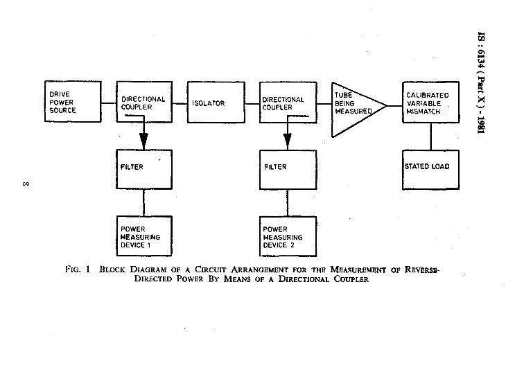
4.1.1 Driving Power ( rf Input Power ) - The rf power input to the crossed- field amplifier tube shall be at the fundamental frequency, unless otherwise stated. This power is measured in the forward arm of a directional coupler with a bandpass filter before the detector. These devices shall be calibrated by substitution methods.
4.1.2 Non.operating ( or Cold) RqTection Coeficient or VSWR - Provision of 7.2 of IS : 6134 ( Part III j-1973* shall apply.
4.1.3 Reverse-Directed Power - Those crossed-field amplifier tubes which do not make use of circuit severs experience at the Input terminals reverse- directed power generated within the tube as well as that reflected from the load. This reverse-directed power may destroy system components unless it is limited to a stated maximum value.
4.1.3.1 Conditions of measurements - The conditions of measurement are as required to measure power and gain. In addition, an isolator and a directional coupler are fitted to the input of the amplifier tube to ensure the required decoupling of the driver and to separate the reverse-directed power. A variable mismatch is also introduced at the output.
If it is desired to analyse the frequencies of the reverse-directed power, suitable filters are required in the power-measuring system, which should be calibrated by substitution method.
4.1.3.2 Measurement -With the tube operating under stated condi- tions in ‘a circuit equivalent to Fig. 1, the reverse-directed power is measured with the aid of directional couplers and filters. The phase of a specified vswr introduced by the variable mismatch is adjusted to obtain a maximum value of reverse-directed power. The result of the measurement is this maximum value.
4.2 Output Power
4.2.1 Provisions of 6 of IS : 6134 ( Part III )-1973* shall apply.
4.3 Control Electrode Figure of Merit - Control electodes in use in injec- ted beam crossed-field amplifier tubes in general have relatively low values of figure of merit and frequently require high bias voltage to turn off.
4.3.1 Conditions of Measurements- The equipment needed for the measurement is indicated in Fig. 2. General conditions as in the measure- ment of output power are used, except for the control-electrode voltage.
4.3.2 Measurement -With the tube connected, as indicated in Fig. 2, with a power meter of suitable sensitivity and operating at power output measurement conditions, except that the control-electrode voltage is ad- justed to give less than the specified output power, the voltage is adjusted
*Methods of measurement on microwave tubes: Part III Amplifier tubes.
7
. .
8 P
FILTER - cl I
I
I I
I I
STATED LOAD
I
FIG. 1 BLOCK DIAGRAM OF A CIRCUIT ARRANGEMENT FOR THE MEASUREMENT OF REVERSB- DIRECTED POWER BY MEANS OF A DIRECTIONAL COUPLER

DRIVE POWER SOURCE
I MOOULATOR
I I
TRIGGER PULSE
\ TUBE
t f VARIABLE DELAY - PULSE I
MODULATOR / 1
L________k_____4
DIRECTIONAL - COUPLER
- MATCHED LOAD
POWER MEASUREMENT
CONTROL ELEC- TRODE SUPPLY
FIG. 2 BLOCK DIAGRAM OF A CIRCUIT ARRANGEMENT FOR THE- MEASUREMENT OF CONTROL ELECTRODE FIGURE! OF MERIT OR OF QUENCH VOLTAGE

IS:6134(PartX)-1981
so as to increase the power to the level prescribed for the measurement. The control-electrode voltage is measured and the figure of merit computed which is equal to the beam-accelerating electrode voltage divided by the control-electrode voltage.
Alternatively, a stated value of control-electrode voltage is applied to the tube and the power output is then measured.
Precaution -Since the reference power level is generally very low compared with the tube capability, the measurements must be made with care to avoid damage to the measurement apparatus.
4.4 Quench Voltage - The application of the quenching pulse to the quench electrode just after completion of a rf drive pulse causes anode current to quench by the capture of unspent electrons just before they would otherwise re-enter the inter-action region. Thus, post-drive oscilla- tion or noise which decreases the operating efficiency is eliminated.
4.4.1 Conditions of Measurement - Figure 2 indicates the equipment needed for the measurement. General conditions as specified for measure- ment of output power, are followed.
4.4.2 Measurement - With the tube connected as in Figure 2 and opera- ting under stated conditions, measure both quench electrode bias and the pulse quench voltage are measured as required to:
a) remain within the quench electrode current and dissipation limits, and
b) arrest the flow of anode current within the stated time.
4.5 Amplifier Measurements - Many emitting-sole crossed-field, amplifiers are unstable in the absence of drive. The manufacturer’s recommendations should be consulted before conducting measurements.
4.5.1 Gain -The crossed-field amplifier tube is operated under all the stated conditions and is adjusted for optimum performance. Gain is computed from measurements of input and output power,
4.5.2 Available Gain at Specified Output Power - Provisions of 4.2 of IS : 6134 ( Part III)-1973* shall apply.
4.5.3 Small-Signal Gain - shall applly.
Provision of 4.3 of IS : 6134 ( Part III)-1973*
4.5.4 Instantaneous Bandwidth 1973* shall apply.
- Provision of 5.1 of IS : 6134 ( Part III )-
*Methods of measurements on microwave tubes: Part III Amplifier tubes.
10

IS : 6134 ( Part x ) - 1981
4.5.5 Spectrum
4.5.5.1 Purpose - The purpose of this test is to verify that the output of the tube is sufficiently well concentrated within a desired range of frequencies. The spectrum of a pulsed or modulated tube has the general appearance shown in Fig. 3 are defined.
4.5.5.2 Procedure - The tube shall be operated in a mismatch unit and specified load ; the vswr of the unit shall be 1.5 : 1 variable over all phases ( half wavelength motion of the mismatch ). The detail specification may specify the distance from the tube to the mismatch unit. If not, the unit shall be as close to the tube as is practicable. The output is sampled and fed to a spectrum analyzer, which will display a spectrum similar to Fig. 3. The mismatch phase is adjusted to the worst position for the parameter being measured ( for example, either widest spectrum or highest side lobes ). If the spectrum analyzer does not have adequate internal calibrators for frequency and amplitude, a marker generator may be used to provide fre- quency calibration points, and a calibrated attenuator may be inserted in the analyzer input line, to measure minor lobe ratio as the difference in readings when the main lobe and highest minor lobe are brought in turn to common reference level.
r MINOR LOBE RATIO
(l/h POWER )
c----_t RF BANOWIOTH
FIG. 3 RF SPECTRUM, ILLUSTRATING DEFINITIONS OF RF BANDWIDTH AND MINOR LOBE RATIO
4.5.5.3 Standard calibration procedures for the load vswr, spectrum analyzer ( and marker generator and attenuator if used) shall be adopted.
4.5.5.4 Precautions - Since the spectrum of a tube is a sensitive func- tion of the pulse shape or modulation delivered by the supply as well as of the performance of the tube, care must be taken to insure that the measure- ment of either RF bandwidth or minor lobe ratio is not degraded by poor performance of the modulator. For short pulse measurements, the spectrum analyzer linearity shall be adequate to ensure that it does not degrade the bandwidth. This may be checked by varying the analyzer centre frequency so as to shift the portion of the sweep used in the display, and observing that the spectrum shape does not change.
11

IS : 6134 (Part X) - 1981
4.5.5.5 Since the theoretical minimum bandwidth is a function of the pulse duration, the detail specification may specify the permissible band- width in terms of duration ( for example, bandwidth = 2S/tp where band- width is in MHz and tp the pbase duration in ms). In this case, the value to be used for tp is the measured value of the current pulse duration, tpc.
4.5.6 Voltage Gain Linearity ( see block diagram Fig. 4 ) - The amplifying electronic device is operated under stated conditions until thermal stability is achieved. An rf carrier is staircase modulated ( equal step-height) between two stated levels. The carrier is passed through the device and then demodulated by a liner detector. The quotient of the minimum to the maximum height of the staircase is the voltage gain linearity.
NOTE - Many crossed-field amplifiers, particularly those with emitting soles, are non- linear reproducers of the rf drive pulse. The manufacturer’s recommendations should be consulted.
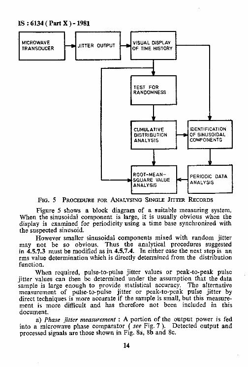
4.5.7 Incidentul Phase Jitter ( Pulse Ampl$ers )
4.5.7.1 Basic data processing procedures and circuits - The overall procedure for analysing the statistical properties of a single jitter record is presented in Fig. 5. Any of the recommended steps may be accompli- shed by either analogue or digital techniques. In either event, the physical jitter parameter must be converted into a voltage analogue or digital format. Figure 6 shows a simplified block diagram of one possible arrange- ment of microwave analogue transducers for time, amplitude, frequency and phase jitter, employing electronic detection circuits. However, other methods using photomultiplier detector circuits which read oscilloscope traces are equally satisfactory and may also be used. The reduction of the measurement data is considerably simplified if extra large power supply filters and other means are used to eliminate non-random components derived from the system.
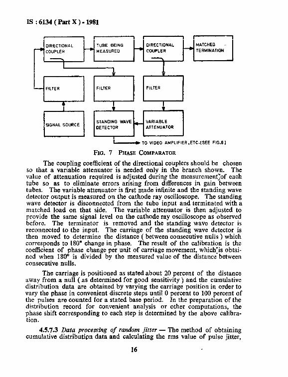
Each of the pulse parameters whose jitter is to be measured is obser- ved with different discriminator means. For phase jitter measurement, a phase comparator as shown in Fig. 7 may be used.
The jitter values determined by these measurements assume no cross-correlation between time, amplitude, frequency or phase jitter. When such cross-correlation can be demonstrated by means beyond the scope of this document, the values can be reduced by quadratic deduction.
4.5.7.2 General measurements (see Fig. 6 )-Data are taken in as many jitter parameters as may be desired in cumulative distribution form, using the described methods ( see 4.5.7.2 a ). These data must then be analysed.
If purely random, the simplified procedures of 4.5.7.3 may be emp- loyed, If periodic contributions are involved, the procedures of 4.5.7.4 should be used. A test for randomness is thus the first test of the data.
12

I3 RF GENERATOR 3 MODULATOR
r
TUBE BEING - MEASURED
DIRECTiONAL HIGH POWER - COUPLER - LOAD
I DISPLAY OR METER
I
L I FIG. 4 TYPICAL BLOCK DIAGRAM OF A CRCUIT FOR MEASURING DIFFERENTIAL GAIN
AND VOLTAGB GAIN LINEARITY
IS :6134(PartX)-1981
MICROWAVE
TRANSDUCER ---, JITTER OUTPUT -#
VISUAL DISPLAY OF TIME HISTORY
RANDOMNESS
I I CUMULATIVE g IDENTlFiCATlON
DISTRIBUTION ANALYSIS
t-4
OF SINUSOIDAL COMPONENTS
I
ROOT-MEAN- SQUARE VALUE
PERIODIC DATA
FIG. 5 PROCEDURE FOR ANALYSING SINGLE JITTER RECORDS
Figure 5 shows a block diagram of a suitable measuring system. When the sinusoidal component is large, it is usually obvious when the display is examined for periodicity using a time base synchronized with the suspected sinusoid.
However smaller sinusoidal components mixed with random jitter may not be so obvious. Thus the analytical procedures suggested in 4.5.7.3 must be modified as in 4.5.7.4. In either case the next step is an rms value determination which is directly determined from the distribution function.
When required, pulse-to-pulse jitter values or peak-to-peak pulse jitter values can then be determined under the assumption that the data sample is large enough to provide statistical accuracy. The alternative measurement of pulse-to-pulse jitter or peak-to-peak pulse jitter by direct techniques is more accurate if the sample is small, but this measure- ment is more difficult and has therefore not been included in this document.
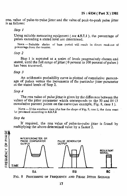
a) Phase jitter measurement : A portion of the output power is fed into a microwave phase comparator ( see Fig. 7 ). Detected output and processed signals are those shown in Fig. 8d, 8b and SC.
14

IS : 6134 ( Part X ) - 1981
I TIME BASE COUNTER
4 4
FIG. 6 ARRANGEMENT FOR MEASURING TIME, AMPLITUDE, FREQUENCY AND PHASE JITTER
4
IS :6134(PartX)-1981
SIGNAL SOURCE STANDING WAVE + VARIABLE
DETECTOR ATTENUATOR
I D TO VIDEO AMPLIFIER ,ETC.ISEE FIG.6 I
FIG. 7 PHASE COMPARATOR
,
DIRECTIONAL TUBE BEING DIRECTIONAL MATCHED .
- COUPLER - MEASURED - COUPLER - TERMINATION
- -
I
4 1
- FILTER FILTER FILTER
The coupling coefficient of the directional couplers should be chosen so that a variable attenuator is needed only in the branch shown. The value of attenuation required is adjusted during the measurement;of each tube so as to eliminate errors arising from differences in gain between tubes. The variable attenuator is first made infinite and the standing wave detector output is measured on the cathode ray oscilloscope. The standing wave detector is disconnected from the tube input and terminated with a matched load on that side. The variable attenuator is then adjusted to provide the same signal level on the cathode ray oscilloscope as observed before. The terminator is removed and the standing wave detector is reconnected to the input. The carriage of the standing wave detector is then moved to determine the distance ( between consecutive nulls ) which corresponds to 180” change in phase. The result of the calibration is the coefficient of phase change per unit of carriage movement, which:is obtai- ned when 180” is divided by the measured value of the distance between consecutive nulls.
The carriage is positioned as stated about 20 percent of the distance away from a null ( as determined for good sensitivity ) and the cumulative distribution data are obtained by varying the carriage position in order to vary the phase in convenient discrete steps until 0 percent to 100 percent of the pulses are counted for a stated base period. In the preparation of the distribution record for convenient analysis or other computations, the phase shift corresponding to each step is determined by the above calibra- tion.
4.5.7.3 Data processing of random jitter - The method of obtaining cumulative distributipn data and calculating the rms value of pulse jitter,
16
IS : 6134 ( Part X) 1981
rms. value of pulse-to-pulse jitter and the value of peak-to-peak pulse jitter is as follows:
Step I
Using suitable measuring equipment (see 4.5.7.1) the percentage of pulses exceeding a stated level are determined.
NOTE -Suitable choice of base period will result in direct read-out of percentage from the counter.
step 2
Step 1 is repeated at a series of levels progressively chosen and stated, until the fulI range of jitter ( 0 percent to 100 percent of pulses ) has been traversed.
Step 3
An arithmetic probability curve is plotted of cumulative percent- age of pulses versus the increments of the particular jitter parameter at the stated levels of Step 2.
Step 4
The rms value of pulse jitter is given by the difference between the values of the jitter parameter which corresponds to the 50 and 84.13 cumulative percent points on the curve (see example, Fig. 8, case 1 ).
NOTE -If the resultant data plot has the shape of Fig. 9, case 2, the data must be processed according to 4.5.7.4
Step 4a
If required, the rms value of pulse-to-pulse jitter is found by multiplying the above-determined value by a factor 2.
INTERFEROMETER OR PHASE COMPARATOR PULSE GENERATOR
OUTPUT
f?IYll
~~ESU;;ANT
II
aA 88 8C
FIG. 8 PROCESSING OF FREQUENCY AND PHASE JITTER SIGNALS
17

IS : 6134 (Part X)*1981
COMPONENT (CASE 2 I-
FIG. 9 CUMULATIVE PERCENT VERSUS TIME AS A JITTER VARIABLE CO-ORDINATE TIMB AND PERCENTAGE
WITH A NORMAL PROBABILITY DISTRIBUTION
Step 4b If required, the peak-to-peak pulse jitter is found by multiplying
the first determined value by a factor 4. NOTE -Where sufficient data have been taken to show that peak-to-peak
measurements ofjitter are correlated with the pulse-to-pulse jitter and that distri- bution is not skewed (see Fig. 10 ) the value of peak-to-peak jitter just determined may be used as a basis ofacceptance.
TIME,t , IN NANOSECONDS
FIG. 10 CUMULATIVE PERCENT VERSUS TIME AS A JITTER VARIABLE WITH ‘SKEW’ DISTRIBUTION
4.5.7.4 Data processing of jitter which includes some periodic contri- bution -The presence of sinusoidal jitter components in otherwise random jitter data may be revealed by a cumulative distribution function for the jitter data. The cumulative distribution plots for random and sinusoidal
18
IS : 6134 ( Part X ) - 1981
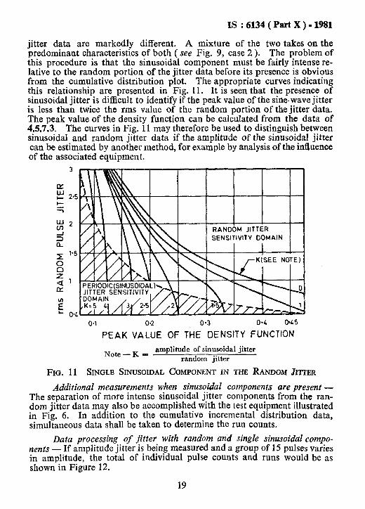
jitter data are markedly different. A mixture of the two takes on the predominant characteristics of both ( see Fig. 9, case 2 ). The problem of this procedure is that the sinusoidal component must be fairly intense re- lative to the random portion of the jitter data before its presence is obvious from the cumulative distribution plot. The appropriate curves indicating this relationship are presented in Fig. 11. It is seen that the presence of sinusoidal jitter is difficult to identify if the peak value of the sine-wave jitter is less than twice the rms value of the random portion of the jitter data. The peak value of the density function can be calculated from the data of 4.5.7.3. The curves in Fig. 11 may therefore be used to distinguish between sinusoidal and random jitter data if the amplitude of the sinusoidal jitter can be estimated by another method, for example by analysis of the influence of the associated equipment.
o-1 0.2 o-3 04 OILS
PEAK VALUE OF THE DENSITY FUNCTtON
Note - K = amplitude of sinusoidal jitter
random jitter
FIG. 11 SINGLE SINUSOIDAL COMPONENT IN THE RANDOM JITTER
Additional measurements when sinusoidal components are present - The separation of more intense sinusoidal jitter components from the ran- dom jitter data may also be accomplished with the test equipment illustrated in Fig. 6. In addition to the cumulative incremental distribution data, simultaneous data shall be taken to determine the run counts.
Data processing of jitter with random and single sinusoidal compo- nents - If amplitude jitter is being measured and a group of 15 pulses varies in amplitude, the total of individual pulse counts and runs would be as shown in Figure 12.
19
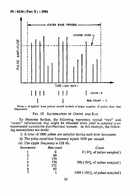
IS : 6134 ( Part X ) i 1981
L STATE0 BASE PERlOOS A I
I - Iii .
_---_
lL
I STATED LEVEL
7 I I I
--B--w_
ill TIME ( SEE NOTE 1
llll 1 1, 1 1 COUNT .8
I 1 RUN COUNT : 2
NOTE -A typical base period would include a larger number of pulses than that illustrated.
FIG. 12 ILLUSTRATION OF COUNT AND RUN
To illustrate further, the following represents typical “run” and “count” information that might be obtained when jitter is sampled in an incremental cumulative distributional manner. In this example, the follow- ing assumptions are made:
i) A total of 1000 pulses are sampled during each level increment. ii) The pulse repetition frequency equals 1000 per second.
iii) The ripple frequency is 120 Hz. Increments Run count Count
0 ( 0% of pulses sampled )
170 176 172 85
1
20
500 ( 50% of pulses sampled )
1000 ( 100% of pulses sampled )

L_I_,. _ ._...~. _ _.__ ._~ _ ..----..- ~-------.-~----.-~--
_-_ ____. .-_-. -..
..-__
IS : 6134 ( Part X ) - 1981
With cumulative “run” and “count” information available, the ran- dom rms. pulse-to-pulse jitter may be computed in the following manner:
Step 1
In the region of 50 percent counts, the average value of the run count is determined. This includes ripple count. ( In the example the average number of runs is equal to 176. )
Step 2
The number resulting from Step 1 is divided by a number which is one-quarter the total number sampled during the count interval to determine a ratio of :
runs with ripple ) x number of pulses sampled
In the example, this ratio is 176 : ( l/4 x 1000 ) or 176 : 250 = 0.7.
Step 3
The ratio R of ripple frequency is established to the pulse repeti- tion frequency of the tube under test. (In the example, this is 120 : 1000 or O-12. ) Then in Fig. 13, the point of intersection with the ratio obtained in-Step 2 is determined. This will enable the rati0.N :
peak value of ripple random jitter
to be found ( by the example N P l-6 ).
Step 4
Using the value of N, a new upper limit for statistical “ sigma ” on the probability versus N graph is determined ( see Fig. 14. In the example, the new limit becomes 82.5).
Step 5
The value of pulse jitter is determined by measuring the jitter between 50 percent and the upper limit obtained from Step 4 on a curve of percent counts versus jitter as illustrated in Fig. 9, case 2.
Step 6
The rms value of random pulse-to-pulse jitter is computed from the value found in Step 5 by multiplying this value by the factor :
4 + 2N2 ( I-cos 2xR) 2 + N’
21

IS : 6134 (Part X ) - 1981
1.6
l*O N =0 N =0*5
0.8 N =l*O
0.6 N = 1.5
N =2-O 0.4
N=2fi
0*2
0 0 0*2 04 0.6 0.6 l*O
R_ RIPPLE FREQUENCY - PULSE t?EPETITIQN FREQUENCY
FIG. 13 RUN TEST TO DETERMINE AMOUNT OF NON-RANDOM JITTER FOR VARIOUS RIPPLE FREQUENCIES AT THE 5074, COUNT LEVEL
where :
N= Peak value of ripple
random jitter
R- ripple frequency
pulse repetition frequency
Data processing of jitter with random and multiple sinusoidal compo- nents - For the vast majority of data, the complex periodic jitter signals are nearly normally distributed so that the presence of more than one sinewave jitter can produce cumulative distribution results which are difficult to distinguish from random jitter data by visual inspection of a cumulative distribution. However, by noting that in this case approximately:
02 (jitter ) = o2 ( random ) + Za* ( periodic ),
practical plots for the separation of a complex periodic component from random jitter data can be developed as shown in Fig. 15. It should be
22

_._ _._
66
76
IS : 6134 ( Part X ) - 1981
I I I I I I I I I
(j t- i i j 1 j
N-PEAK VALUE OF RIPPLE
RANDOM JITTER
FIG. 14 DETERMINATION OF UPPER o LIMIT TO COMPUTE RMS JITTER MEASURED
noted that for an amplitude of the complex periodic component 2 to 24 times the rms value of pulse jitter is about 20 percent to 30 percent greater than the rms value of the random pulse jitter.
4.5.7.5 Precautions a) The video bandwidth of all detector circuits is quite important to
obtain reliable data. Bandwidths suited for one-tenth of the pulse width are generally adequate.
b) In the measurement of frequency and/or phase jitter, the non-line- arity characteristic of the detector results in a loss of sensitivity of the system adjusted for perfect cancellation. It is usually found convenient to adjust the attenuator so that the signal is approxi- mately 10 percent of the value at infinite attenuation in order to obtain sufficient amplitude dispersion in the detected output so that gate generators can effectively discriminate between levels.
23

IS : 6134 ( Part X ) - 1981
o-5 1 l+ , 2 2.5 3
rms PULSE JITTER
Note - Values of K where K = amplitude of sinusoidal jitter
random jitter
FIG. 15 MULTIPLE SINUSOIDAL SIGNALS IN THE RANDOM JITTER
c) Measurements on devices may not result in normal distributions ( whose rms values are easily determined ) if the power source con- tains coherent signal ripple or if the electron source is subject to ac magnetic fields. It may thus be found convenient to use more filter capacitance during these measurements. However, the possibility that the extra energy storage could harm personnel or damage the tube must be adequately guarded against.
4.5.8 AM- PM conversion Coejicient and Compression Factor ( see Fig. 16)
4.5.8.1 Theory - AM - PM conversion and compression in an amplifier may be assessed by applying an input consisting of :
i) carrier, frequency f, amplitude A, power level Aa, and ii) simulated sideband, frequencyf,, amplitude S, power level S2.
For simplicity of working, the level difference between carrier and side- band, is chosen to be at least 30 dB and the sideband amplitude S is taken as unity.
The spectrum of this signal, in relative power levels, is represented in Fig. 16a.
24

IS :6134(PartX)-1981
___ ----_a-
f %
30 dB MINIMUM. &
-------L1:
fc f, FREQUENCY FRi%UEN.CY
I6A Input signal 168 Output signal attenuated to make the level at te identical
to As input
FIG. 16 INPUT AND OUTPUT SIGNALS FOR SINGLE SIDEBAND METHOD OF MEAWRIIVG COMPRESSION AND AM-PM CONVERSION
When the signal is applied to a non-linear amplifier, the spectrum of the output is different, as seen in Fig. 16b. The sideband level is now S, and a new sideband of level S’s appears at fs.
To assess the magnitude of this effect, S, and S, are compared with S and, since S has been taken as unity, they become dimensionless fractions.
Using these fractions, it can be shown that the AM - PM conversion coefficient Kp, in degrees per decibel, is given by :
&,c 13*16+ -(‘+‘;-“)
The compression factor C is given by :
c= 1-(S,“-S$)
458.2 Methods of measurement
a) Method Z
The device is operated under stated conditions and driven by input signals fc and fi as indicated in Fig. 16a.
The output power of the device is attenuated to display the level of the signal at fc at the same level as at the input, and the spectrum as in Fig. 16b is observed.
25
IS : 6134 (Part X ) - 1981
The values of .S2, and S”, are computed from the formula:
s,’ = 1 - R
antilog loF
where R is the difference in decibels between the power levels of S* and S,.
The computed values of Szl and S’, are then used in the formulae of 458.1 to calculate Kp and C.
b) Method 2
This method for the measurement of AM - PM conversion coefficient is sometimes convenient for use at lower frequencies, but gives somewhat less accurate results.
The tube is operated under stated conditions. The phase angle of the rf output voltage relative to the phase of the input voltage is observed. The amplitude of the rf input voltage is then changed at a rate that pre- cludes thermal effects, and the maximum variation in phase angle between output and input voltages is noted. The measured value of the AM - PM transfer is a quotient, expressed in degrees per decibel of (1) the maximum change of the phase angle to (2) the change of the driving power when this change is so small that a further reduction has a negligible effect on the quotient to be measured.
Because the AM-PM conversion coefficient depends upon the power level, it is necessary to state the input at which the measurement is made.
Precautions
This measurement is sensitive to voltage fluctuations, which therefore must be kept small if their effect on the measured result is to be negligible.
4.5.9 Phase Sensitivity to Voltage or Current-Provision of 9 of IS : 6134 ( Part IIl )-1973* shall apply.
4.6 Reproducibility of Stated Variable - The crossed-field amplifier tube is adjusted for optimum performance under stated conditions and after thermal equilibrium has been reached, the stated variable is measured. The operating conditions of voltage and drive are then maintained at constant values for the remainder of the measurement.
A second set of stated conditions, usually the turn-off of beam power and drive only, is maintained for a stated period. The original conditions
1 i 6
*Methods of measurements on microwave tubes: Part III Amplifier tubes.
26

Is :6134(Part X)-1981
are then restored and the tube is operated until thermal equilibrium is again achieved. The change in the value of the stated variable is then measured.
NOTE --This measurement is necessary because the thermal expansion of the line ( slow-wave structure ) and role structures may cause non-reproducible transients during warm-up.
4.7 Mismatch Stability
4.7.1 Provisions 10.3 of IS : 6134 ( Part III )-1973* shall apply in addition to the following:
The crossed-field amplifier tube is operated in accordance with the stated conditions while a stated value of reflection coefficient ( or vswr ) is varied through all phases. The tube is considered to be satisfactory if it meets the required performance under these stated conditions.
4.8 .Noise - Provision of IS : 6134 ( Part V )-19807 shall apply.
4.9 Unwanted Output Power
4.9.1 Measurement of Unwanted Oscillations with Drive - The crossed- field amplifier tube is operated under stated conditions, adjusted for opti- mum bandwidth and power. The output spectrum is examined over a stated range and the power of all non-harmonic signals is measured relative to the output power at the carrier frequency.
4.9.2 Measurement of Unwanted Oscillations without Drive - Unwanted oscillations, especially those which occur in the absence of drive, often have frequencies at or near the cut-off frequency of the slow-wave structure or output waveguide ( whichever is higher in frequency ), because at cut-off the amplifier gain and circuit impedance are very high, resulting in low values of starting current.
4.9.3 Precaution : Care should be taken to ensure that the cut-off frequency of’ the transmission system is beyond that of the slow-wave structure or that the transmission system is matched down to the cut-off frequency.
NOTE -Many spectrum analysers generate responses having frequencies equal to the sums and differences of integral multiples of the local oscillator frequency and the fre- quencies being measured. It may be necessary to plot these for values up to about the tenth harmonic in order to be able to exclude there “instrumental spunous” responses from tbe measurement.
4.9.4 Intermodulation Output ( Non-linearity )
4.9.4.1 Zntermodulation
General methods
The amplifying device is operated under stated conditions. Stated carriers are then applied simultaneously. The output spectrum is studied
‘Methods of measurements on microwave tube: Part III Amplifier tubes. *Methods of measurements on microwave tuber: Part V Parasitic noise.
.
27

IS:6134(PartX)-1981
and each intermodulation product within the .stated bandwidth, or the intermodulation product greater than a stated power, is measured.
For each intermodulation product, the result is oxprossed in decibels relative to a stated power level.
Precautions
To avoid distortion by intermodulation in the driving source, the combination of the carriers is achieved by hybrids and isolators or attenua- tors, as shown in Fig. 17. Intermodulation products of the input shall be at least 10 dB lower in amplitude than the smallest intermodulation product to be measured.
Harmonic outputs will in general be present and should not be ignored. Their magnitude may be highly dependent on the associated circuit. It may be necessary to use low-pass filters to remove them.
Two-frequency ( tone ) method ( S.S.B. )
The amplifying electronic device is operated under stated conditions. Two carriers of equal power of frequencies fi and f, ( each equal to half the stated input power ) are used at, the input. If non-linearity exists in the device, intermodulation products occur at the output with frequencies pf f qfe. The difference in level, expressed in decibels, between the inter- modulation product with the highest level and the lower of the carrier levels is the intermodulation ratio. An example is given in Fig. 18.
NOTE 1 -The greatest intermodulation product does not necessarily occur at the highest peak envelope power level.
NOTE 2 1 If the intermodulation products at opposite sides of the two tones are different in amplitude, the higher value is taken. This gives the lowest intcrmodula- tion ratio.
Three-frequency ( tone ) method ( TV)
The amplifying electronic device is operated under stated conditions. Three frequencies fa, fb, fC are used. The power levels, the frequency spacings of the three frequencies and the reference level shall be stated. The largest intermodulation product fi within a stated band, is measured with reference to the stated reference level ( peak synchronization level ) and expressed in decibels ( see Fig. 19 ).
28

GENERATOR H VARIABLE ATTENUATOR t
1J 1 1
GENERATOR
t 2
t r
- ISOLATOR - MATCHEO LOAD
1
-
HYBRID
HY BRIO I)
.
GENERATOR _ VARIABLE ATTENUATOR
- ISOLitTOR - _ LEVEL SET ATTENUATOR -
3 , 3 3
Fro. 17 ARRANGEMENT TO AVOID DISTORTION OF DNMNO SIGNALS BY I~I~UH~LWLATION
GENERATOR
1 t; . .
E w a
h

IS:6134(PartX)-1981
----_
LEVEL DIFFERENCE (INTERMODULATION
RATIO)
-- -_ r
I!__
+---STATED FREQUENCY BAND --_cI
FIG. I8 INTERMODULATION : TWO-FREQUENCY METHOD
------ - REFERENCE LEVEL -_---------
T
-l---
1
LEVEL DliFERENCE
(INTERMODULATION
----
i fa f b fi f c ;
id----- STATED FREQUENCY BAND --i
FIG. 19 a INTERMODULATION : THREE-FREQUENCY METHOD
30

IS:6134(Part X)*1981
APPENDIX A ( Clause 0.3 )
THEORETICAL WORKING OF CROSSED-FIELD AMPLIFUER TUBES
A-l. CROSSED-FIELD INTERACTION
A-l.1 In the presence of crossed-fields, neglecting space charge forces, electrons move in the direction which is mutually perpendicular to both the applied field vectors, at a velocity equal to the ratio of the fields ( that is,
v : =---, where V is the electron velocity, E is the static electric field intensity
and B is the static magnetic induction ). When this velocity is made synchron- ous with that of a space harmonic travelling on the anode circuit, energy exchange takes place. As the electron moves towards the anode under the influence of the rf field, its velocity and kinetic energy remain approxi- mately constant, but it transfers incremental potential energy to the synchronous-circuit wave. Under the large-signal and dense space-charge conditions of most crossed-field amplifier the velocities of both the circuit wave and beam are modified and an excess voltage is required to sustain operation.
A-2. CROSSED-FIELD AMPLIFIER TUBES
A-2.1 The crossed-field amplifier family of microwave tubes exists in many configurations which represent combinations of one from each of the following:
4
b)
4
The electron beam is injected by an electron gun or derived from an emitting sole or both. A separate heating source for the sole may or may not be required. The unspent portion of the electron beam either re-enters the interaction region at the input or as collected at theexit of the interaction region. The electron beam interacts with either a backward-wave or a forward-wave circuit.
Each of these parameters has its own effect on the tube characteristics. In general, forward-wave tubes have greater bandwidth and lower efficiency than backward-wave tubes.
A-3. INJECTED BEAM TUBES
A-3.1 Injected beam devices using thin beams are in general high-impedance electron tubes. The beam geometry permits the use of circuit severs and thus working gains of up to 30 dB are possible. Tubes of this type, designed for forward-wave interaction. may have bandwidths of greater than an octave together with an efficiency of greater than 30 percent.
31

IS:6134(PartX)-1981
A-33 The beam current, in an injected beam tube, is controlled by modulating the voltage on the beam-control electrode incorporated in the electron gun. Some of the electrons which are emitted fail to interact and thus they pass through the tube without adding to the rf power. It is sometimes possible to use a collector at or near cathode potential to return the unused electrons to the power supply, thus recovering a portion of the energy that would otherwise be lost.
A-4. EMI’ITING SOLE TUBES
A-4.1 An emitting sole having a large area results in a relatively low value of beam impedance and is appropriate to moderate to high-power tubes. Such a structure results in a multiple-velocity beam and gains of typically 13 dB to 20 dB. Tubes of this type designed for interaction with forward- waves tend to have lower efficiency but wider bandwidth. The eBciency of interaction may be increased by causing the electron beam to re-enter the interaction region at the input, thus forming a re-entrant beam device. A-4.2 The emitting sole may be heated so that the beam is derived from a primary emission of electrons. Such tubes may be unstable in the absence of rf drive and if used under pulse conditions operate satisfactorily only if the beam current is pulsed by cathode pulses whose duration is contained entirely within that of the rf pulse; if the beam pulse duration extends beyond that of the rf pulse, undesirable signals may be developed or the tube may be damaged. A-1.3 Certain types of cold-sole pulsed crossed-field amplifier tubes operate with continuous beam voltages. The electron beam which may be re-entrant non-re-entrant is derived from secondary electrons emitted from the sole in the presence of adequate rf drive. In the absence of adequate drive, the beam current ceases and no amplification takes place, even though the synchronous voltages are still applied. Satisfactory operation may be obtained over a range of rf drive. At lower values, the secondary emission may be inadequate to provide useful amplification, while at higher values undesirable moding may occur. A-4.4 In those tubes which employ a re-entrant beam with internal feedback to increase efficiency, the beam current will not cease when drive power ceases, because the re-entering electrons are sufficient to cause wide- band noise. Thus, a normally non-intercepting electrode ( called the quench electrode) must be added to the structure to capture such re- entering electrons. An appropriate voltage pulse applied to this electrode at the end of the rf pulse will cut off the beam current without the necessity of cathode modulation.
A-5. DRIVE POWER LEVEL
A-5.1 The drive power levels of crossed-field amplifiers depend upon the output power, gain and efficiency. They are generally in the range of tens of watts to 50-100 kilowatts.
32

iNDIAN STANiBARDS
ON
ELECTRON TUBES
IS : 1885 (Part IV/Set 1 )-I973 Electrotechnical vocabulary: Part IV Electron tubes, SCC*
tion 1 Common terms ( first re~vision ) 1885 ( Part IV/Set 2 )-1973 Electrotechnical vocabulary : Part IV Electron tubes, Sec-
tion 2 X-ray tubes ( jirst revision ) 1885 ( Part IV/See 3 )-1970 Electrotechnical vocabulary : Part IV Electron tubes, Sec-
tion 3 Microwave tubes 1885 (Part IV/Set 4 )-1970 Electrotechnical vocabulary : Part IV Electron tubes, Sec-
tion 4 Cathode-ray tubes 1885 ( Part IV/SW 5 )-1972 Electrotechnical vocabulary: Part IV Electron tubes, SCC-
tion 5 Pulse terms 1885 (Part IV/Set 6 )-1972 Electrotechnical vocabulary: Part IV Electron tubes, Sec-
tion 6 Noise in Microwave tubes 1885 ( Part IV/Set 7 )-1973 Elcctrotechnical vocabulary : Part IV Electrone tubes Sec-
tion 7 Camera tubes 1885 I Part IV/Set 8 )-1973 Electrotechnical vocabularv: Part IV Electrone tubes Sec-
tion 8 Photo-sensitive devices 2032 ( Part IX)-1969 Graphical symbols used in clectrotechnology : Part IX Electron
tubes ( other than microwave tubes) 2032 ( Part XIII )-1971 Graphical symbols used in electrotechnology : Part XIII
Microwave tubes 2597 ( Part 11-1964 Code of nracticc for the use of electronic valves: Part I Commercial
receiving valves _ 2597 ( Part II )-1967 Code of practice for the use of electronic valves : Part II Special
quality receiving valves 2597 ( Part III )-1969 Code of practice for the use of electronic valves: Part III
Transmitting and industrial valves 2597 (Part IV)-1970 Code of practice for the USC of electronic valves : Part IV
Cathode-ray tubes 2597 (Part V )-1971 Code of practice for the use of clcctronic valves : Part V Ractifiers
and thyratrons 2684 ( Part I )-1972 Dimensions of electronic valves: Part I Miniature g-pin nova1
2684 ( Part II )-1972 Dimensions of electronic valves : Part II Miniature 7-pin type ( jrsr revision )
2684 ( Part III )-1971 Dimensions of electronic valves : Part III Octal base type 2684 (Part IV)-1971 Dimensions of electronic valves: Part IV Mapnoval base type 2684 ( Part V)-1972 Dimensions of electronic valves: Part V Local base type 3154-1965 Specification for X-ray tubes, diagnostic type 4096-1973 Method of measurement of optical focal spot size of X-ray tubes (J;IJ~ rcviJion )
4147- 1967 Method of measurements on conventional receiving electronic valves 4579-1968 Methods of measurements on television picture tubes 4697-1968 Methods of measurements on Geiger-Miller counter tubes 5323-1969 Letter symbols and abbreviations for electron tubes and valves 5627-1970 Methods of measurements on cathode-ray display tubes 5840 ( Part I )-1970 Dimensions of cathode-ray tubes: Part I Tube outlines 5840 (Part II )-1970 Dimensions of cathode-ray tubes: Part II Bases 5840 ( Part III)-1970 Dimensions ofcathode-ray tubes: Part III EHT terminals 6 134 ( Part I )- 1978 Methods of measurements of electrical characteristics of micrawave
tubes: Part I Common to all microwave tubes ( prst r&Jim ) [ Superseding IS: 6134 ( Part I/Set 1 )-1971 and IS : 6134 ( Part I/See 2 ) ]
6134 ( Part II )-1973 Methods of measurement of electrical characteristics of microwave tubes : Part II Oscillator tubes
6134 ( Part III )-1973 Methods of measurement ofelectrical characteristics of microwave tubes : Part III Amplifier tubes
6134 ( Part IV )-1977 Methods of measurement of electrical characteristics ofmicrowave tubes: Part IV Magnetrons
6134 ( Part V )-1980 Methods of measurement of electrical characteristics of microwave tubes : Part V Parasitic noise
6134 ( Part VI )-1981 Methods of measurement of electrical characteristics of microwave tubis : Part VI Low-power oscillator klystrons
6134 ( Part VII ) 1981 Methods of measurement of electrical characteristics of micro- wave tubes : Part VII High-power klystrons
6134 ( Part VIII)-1981 Methods of measurement of electrical characteristics of micro- wave tubes : Part VIII Gas-filled microwave switching devices
6134 ( Part IX )-1981 Methods of measurement of electrical characteristics of microwave tubes : Part IX Backward-wave oscillator tubes-‘0’ type
6134 ( Part X 1-1981 Methods of measurement of electrical characteristics of microwave
6136-1971 6214-1971 6567-1972
6568-l 972 6576-1972 6577-1972
tubes : Part X Crossed-field amplifier tubes Basic requirements for cathode-ray tubes Phosphors for cathode-ray tubes Radiation protection for an X-ray tube in a protective tube-housing, operat- ing between 10 kV and 400 kV Implosion protection for TV picture tubes Methods of measurements on gas filled cold cathode indicator tubes Methods of measurements on gas cold cathode voltage stabilizing and voltage reference tubes Dimensions for high tension cable terminations for X-ray tubes Dimensions for high tension receptacles for X-ray tubes +c_ificatio_n for X-ray tube shield .
6757-1972 6758-1972 7012-1973 71441973 Methods of measurements on camera NDCS
7146 ( Part I )-I973 Methods of measurements on photosensitive devices: Part I Basic considerations
7146 ( Part II )-1974 Methods of measurements on photosensitive devices: Part II Photo- tuber
7146 ( Part III )-1974 Methods of measurements on photosensitive devices: Part III Photoconductive cells for use in the visible spectrum
7146 (Part IV )-1974 Methods of measurements on photosensitive devices: Part IV Photomultipliers
8319 ( Part I )-1977 Dimensions of indicator tubes: Part I Tube type 1 8319 ( Part II )-I977 Dimcsions of indicator tubes: Part II Tube Type 2 8319 ( Part III )-1973 Dimensions of indicator tubes : Part III Tube type 3 8319 ( Part IV )-I979 Dimensions of indicator tubes : Part IV Tube Type 4 8441-1977 Methods of measurements on incidental X-radiation from electron tubes 9383 ( Part I )-I979 Dimensions of sign indicator tubes : Part I Tube type 1 9383 ( Part II )-I979 Dimensions of sign indicator tubes : Part II Tube type 2 9492-1980 Methods of measurement of RF/microwave leakage from integral circuit
9883-1981 electron tubes Photometric and colorometric methods of mcauremcnts of the eight emitted by a cathode-ray tube screen