Embed Size (px)
Citation preview
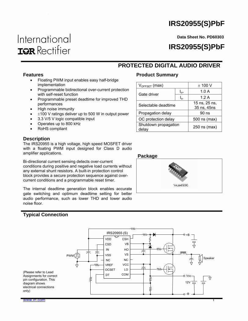
IRS20955(S)PbF
www.irf.com 1
IRS20955(S)PbF
PROTECTED DIGITAL AUDIO DRIVER Features
• Floating PWM input enables easy half-bridge implementation
• Programmable bidirectional over-current protection with self-reset function
• Programmable preset deadtime for improved THD performances
• High noise immunity • ±100 V ratings deliver up to 500 W in output power • 3.3 V/5 V logic compatible input • Operates up to 800 kHz • RoHS compliant
Description The IRS20955 is a high voltage, high speed MOSFET driver with a floating PWM input designed for Class D audio amplifier applications. Bi-directional current sensing detects over-current conditions during positive and negative load currents without any external shunt resistors. A built-in protection control block provides a secure protection sequence against over-current conditions and a programmable reset timer. The internal deadtime generation block enables accurate gate switching and optimum deadtime setting for better audio performance, such as lower THD and lower audio noise floor.
Product Summary
VOFFSET (max) ± 100 V Io+ 1.0 A
Gate driver Io- 1.2 A
Selectable deadtime 15 ns, 25 ns, 35 ns, 45ns
Propagation delay 90 ns OC protection delay 500 ns (max) Shutdown propagation delay 250 ns (max)
Package
Typical Connection (Please refer to Lead Assignments for correct pin configuration. This diagram shows electrical connections only)
IRS20955 (S)
12V
VDD
IN
CSD
VSS
COMOCSET LO
VCC
HO
VS
DT
CSH
VB
-B
Vcc
Speaker
+B
PWM
VREFNC NC
Data Sheet No. PD60303
IRS20955(S)PbF
www.irf.com 2
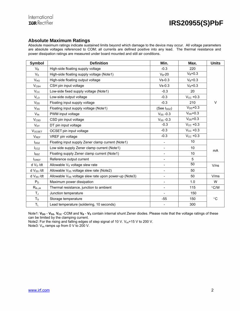
Absolute Maximum Ratings Absolute maximum ratings indicate sustained limits beyond which damage to the device may occur. All voltage parameters are absolute voltages referenced to COM; all currents are defined positive into any lead. The thermal resistance and power dissipation ratings are measured under board mounted and still air conditions. Symbol Definition Min. Max. Units
VB High-side floating supply voltage -0.3 220 VS High-side floating supply voltage (Note1) VB-20 VB+0.3
VHO High-side floating output voltage Vs-0.3 VB+0.3 VCSH CSH pin input voltage Vs-0.3 VB+0.3 VCC Low-side fixed supply voltage (Note1) -0.3 20 VLO Low-side output voltage -0.3 VCC +0.3 VDD Floating input supply voltage -0.3 210 VSS Floating input supply voltage (Note1) (See IDDZ) VDD+0.3
VIN PWM input voltage VSS -0.3 VDD+0.3
VCSD CSD pin input voltage VSS -0.3 VDD+0.3
VDT DT pin input voltage -0.3 VCC +0.3
VOCSET OCSET pin input voltage -0.3 VCC +0.3
VREF VREF pin voltage -0.3 VCC +0.3
V
IDDZ Floating input supply Zener clamp current (Note1) - 10
ICCZ Low side supply Zener clamp current (Note1) - 10 IBSZ Floating supply Zener clamp current (Note1) - 10
IOREF Reference output current - 5
mA
d VS /dt Allowable VS voltage slew rate - 50
d VSS /dt Allowable VSS voltage slew rate (Note2) - 50 V/ns
d VSS /dt Allowable VSS voltage slew rate upon power-up (Note3) - 50 V/ms PD Maximum power dissipation - 1.0 W
Rth,JA Thermal resistance, junction to ambient - 115 °C/W TJ Junction temperature - 150 TS Storage temperature -55 150 TL Lead temperature (soldering, 10 seconds) - 300
°C
Note1: VDD - VSS, VCC -COM and VB - VS contain internal shunt Zener diodes. Please note that the voltage ratings of these can be limited by the clamping current. Note2: For the rising and falling edges of step signal of 10 V. Vss=15 V to 200 V. Note3: Vss ramps up from 0 V to 200 V.
IRS20955(S)PbF
www.irf.com 3
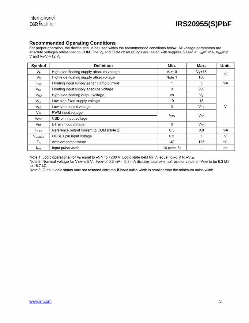
Recommended Operating Conditions For proper operation, the device should be used within the recommended conditions below. All voltage parameters are absolute voltages referenced to COM. The VS and COM offset ratings are tested with supplies biased at IDD=5 mA, VCC=12 V and VB-VS=12 V. Symbol Definition Min. Max. Units
VB High-side floating supply absolute voltage VS+10 VS+18 VS High-side floating supply offset voltage Note 1 100
V
IDDZ Floating input supply zener clamp current 1 5 mA VSS Floating input supply absolute voltage 0 200 VHO High-side floating output voltage Vs VB VCC Low-side fixed supply voltage 10 18 VLO Low-side output voltage 0 VCC VIN PWM input voltage
VCSD CSD pin input voltage VSS VDD
VDT DT pin input voltage 0 VCC
V
IOREF Reference output current to COM (Note 2) 0.3 0.8 mA VOCSET OCSET pin input voltage 0.5 5 V
TA Ambient temperature -40 125 °C IPW Input pulse width 10 (note 3) - ns
Note 1: Logic operational for VS equal to –5 V to +200 V. Logic state held for VS equal to –5 V to –VBS. Note 2: Nominal voltage for VREF is 5 V. IOREF of 0.3 mA – 0.8 mA dictates total external resistor value on VREF to be 6.3 kΩ to 16.7 kΩ. Note 3: Output logic status may not respond correctly if input pulse width is smaller than the minimum pulse width
IRS20955(S)PbF
www.irf.com 4
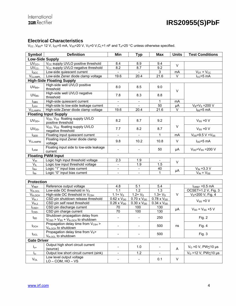
Electrical Characteristics VCC ,VBS= 12 V, IDD=5 mA, VSS=20 V, VS=0 V,CL=1 nF and TA=25 °C unless otherwise specified. Symbol Definition Min Typ Max Units Test Conditions Low-Side Supply
UVCC+ VCC supply UVLO positive threshold 8.4 8.9 9.4 UVCC- VCC supply UVLO negative threshold 8.2 8.7 9.2 V
IQCC Low-side quiescent current - - 3 mA VDT = VCC VCLAMPL Low-side Zener diode clamp voltage 19.6 20.4 21.6 V ICC=5 mA
High-Side Floating Supply UVBS+
High-side well UVLO positive threshold 8.0 8.5 9.0
UVBS- High-side well UVLO negative threshold 7.8 8.3 8.8
V
IQBS High-side quiescent current - - 1 mA
ILKH High-side to low-side leakage current - - 50 µA VB=VS =200 V VCLAMPH High-side Zener diode clamp voltage 19.6 20.4 21.6 V IBS=5 mA Floating Input Supply
UVDD+ VDD, VSS floating supply UVLO positive threshold 8.2 8.7 9.2 VSS =0 V
UVDD- VDD, VSS floating supply UVLO negative threshold 7.7 8.2 8.7
V VSS =0 V
IQDD Floating input quiescent current - - 1 mA VDD=9.5 V +VSS
VCLAMPM Floating input Zener diode clamp voltage 9.8 10.2 10.8 V IDD=5 mA
ILKM Floating input side to low-side leakage current - - 50 µA VDD=VSS =200 V
Floating PWM Input VIH Logic high input threshold voltage 2.3 1.9 - VIL Logic low input threshold voltage - 1.9 1.5 V
IIN+ Logic “1” input bias current - - 40 VIN =3.3 V IIN- Logic “0” input bias current - - 1 µA VIN = VSS
Protection
VREF Reference output voltage 4.8 5.1 5.4 IOREF =0.5 mA Vth,OCL Low-side OC threshold in VS 1.1 1.2 1.3 OCSET=1.2 V, Fig. 3 Vth,OCH High-side OC threshold in VCSH 1.1+ VS 1.2+ VS 1.3+ VS VS=200 V, Fig. 4 Vth,1 CSD pin shutdown release threshold 0.62 x VDD 0.70 x VDD 0.78 x VDD Vth,2 CSD pin self reset threshold 0.26 x VDD 0.30 x VDD 0.34 x VDD
V VSS =0 V
ICSD+ CSD pin discharge current 70 100 130 ICSD- CSD pin charge current 70 100 130 µA VSD = VSS +5 V
tSD Shutdown propagation delay from VCSD > VSS + Vth,OCH to shutdown - - 250 Fig. 2
tOCH Propagation delay time from VCSH > Vth,OCH to shutdown - - 500 Fig. 4
tOCL Propagation delay time from VS> Vth,OCL to shutdown - - 500
ns
Fig. 3
Gate Driver Io+
Output high short circuit current (source) - 1.0 - VO =0 V, PW<10 µs
Io- Output low short circuit current (sink) - 1.2 - A
VO =12 V, PW<10 µs
VOL Low level output voltage LO – COM, HO – VS - - 0.1 V
IRS20955(S)PbF
www.irf.com 5
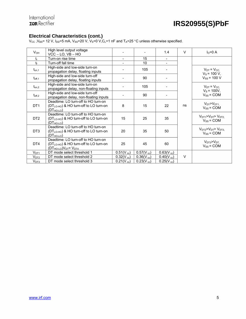
Electrical Characteristics (cont.) VCC ,VBS= 12 V, IDD=5 mA, VSS=20 V, VS=0 V,CL=1 nF and TA=25 °C unless otherwise specified.
VOH High level output voltage VCC – LO, VB – HO - - 1.4 V IO=0 A
tr Turn-on rise time - 15 - tf Turn-off fall time - 10 -
ton,1 High-side and low-side turn-on propagation delay, floating inputs - 105 -
toff,1 High-side and low-side turn-off propagation delay, floating inputs - 90 -
VDT = VCC, VS = 100 V, VSS = 100 V
ton,2 High-side and low-side turn-on propagation delay, non-floating inputs - 105 -
toff,2 High-side and low-side turn-off propagation delay, non-floating inputs - 90 -
VDT = VCC, VS = 100V, VSS = COM
DT1 Deadtime: LO turn-off to HO turn-on (DTLO-HO) & HO turn-off to LO turn-on (DTHO-LO)
8 15 22 VDT>VDT1, VSS = COM
DT2 Deadtime: LO turn-off to HO turn-on (DTLO-HO) & HO turn-off to LO turn-on (DTHO-LO)
15 25 35 VDT1>VDT> VDT2, VSS = COM
DT3 Deadtime: LO turn-off to HO turn-on (DTLO-HO) & HO turn-off to LO turn-on (DTHO-LO)
20 35 50 VDT2>VDT> VDT3, VSS = COM
DT4 Deadtime: LO turn-off to HO turn-on (DTLO-HO) & HO turn-off to LO turn-on (DTHO-LO)VDT= VDT4
25 45 60
ns
VDT3>VDT, VSS = COM
VDT1 DT mode select threshold 1 0.51(V cc) 0.57(V cc) 0.63(V cc) VDT2 DT mode select threshold 2 0.32(V cc) 0.36(V cc) 0.40(V cc) VDT3 DT mode select threshold 3 0.21(V cc) 0.23(V cc) 0.25(V cc)
V
IRS20955(S)PbF
www.irf.com 6
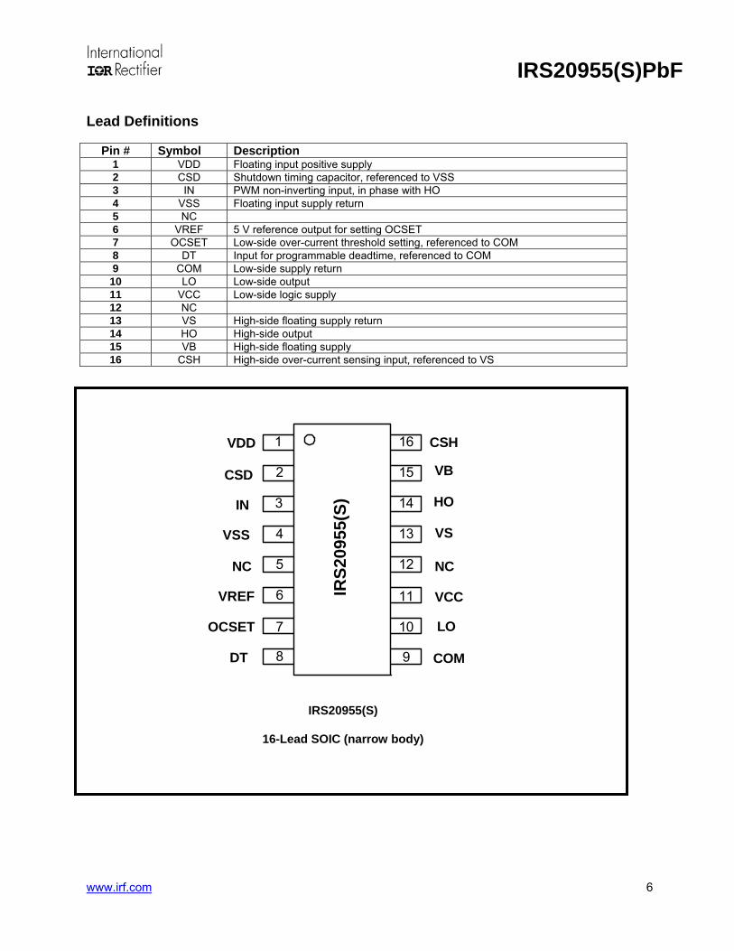
Lead Definitions
Pin # Symbol Description 1 VDD Floating input positive supply 2 CSD Shutdown timing capacitor, referenced to VSS 3 IN PWM non-inverting input, in phase with HO 4 VSS Floating input supply return 5 NC 6 VREF 5 V reference output for setting OCSET 7 OCSET Low-side over-current threshold setting, referenced to COM 8 DT Input for programmable deadtime, referenced to COM 9 COM Low-side supply return 10 LO Low-side output 11 VCC Low-side logic supply 12 NC 13 VS High-side floating supply return 14 HO High-side output 15 VB High-side floating supply 16 CSH High-side over-current sensing input, referenced to VS
1
2
3
4
5
6
7
8
16
15
14
13
12
11
10
9
IRS2
0955
(S)
VDD
IN
CSD
VSS
OCSET
DT
VREF
COM
LO
VCC
HO
VS
CSH
VB
NC NC
IRS20955(S)
16-Lead SOIC (narrow body)
IRS20955(S)PbF
www.irf.com 7
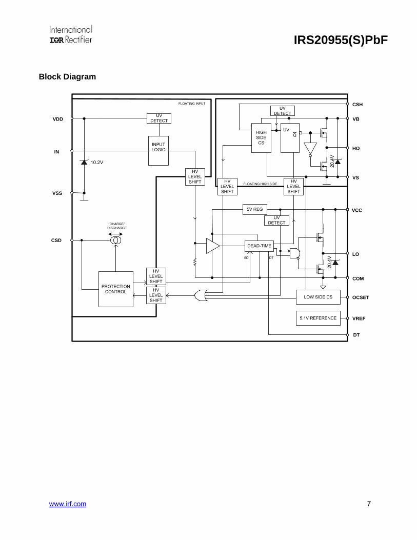
Block Diagram
HIGH SIDE CS
VB
HO
VS
IN
LOW SIDE CS
CSD
UV Q
UV DETECT
DEAD-TIME
VCC
LO
COM
VDD
VSS
CSH
PROTECTIONCONTROL
SD
OCSET
UV DETECTUV
DETECT
CHARGE/DISCHARGE
HVLEVEL SHIFT
HVLEVEL SHIFT
HVLEVEL SHIFT
FLOATING INPUT
FLOATING HIGH SIDE
HVLEVEL SHIFT
HVLEVEL SHIFT
5V REG
DT
DT
INPUT LOGIC
10.2V
20.4
V20
.4V
VREF5.1V REFERENCE
IRS20955(S)PbF
www.irf.com 8
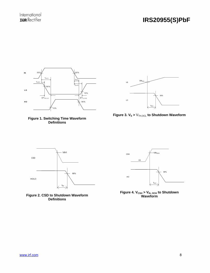
50% 50%
toff(L)ton(L)
90%
10%
90%
10%
D T HO -LO
toff(H )
IN
LO
H O
ton(H )
D T LO-H O
Figure 1. Switching Time Waveform Definitions
Vth1
tSD
90%
CSD
HO/LO
Figure 2. CSD to Shutdown Waveform Definitions
VthOCL
tOCL
90%
VS
LO
Figure 3. VS > VTH,OCL to Shutdown Waveform
VthOCH
tOCH
90%
CSH
HO
VS
Figure 4. VCSH > Vth, OCH to Shutdown Waveform
IRS20955(S)PbF
www.irf.com 9
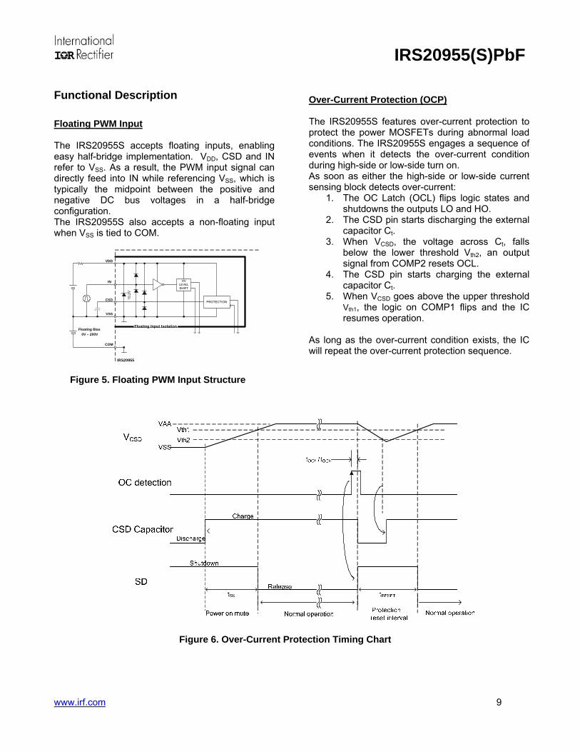
Functional Description
Floating PWM Input The IRS20955S accepts floating inputs, enabling easy half-bridge implementation. VDD, CSD and IN refer to VSS. As a result, the PWM input signal can directly feed into IN while referencing VSS, which is typically the midpoint between the positive and negative DC bus voltages in a half-bridge configuration. The IRS20955S also accepts a non-floating input when VSS is tied to COM.
IN
VDD
VSS
10.2
V
HVLEVEL SHIFT
CSD PROTECTION
Floating Input Isolation
COM
Floating Bias
IRS20955
0V – 200V
Figure 5. Floating PWM Input Structure
Over-Current Protection (OCP) The IRS20955S features over-current protection to protect the power MOSFETs during abnormal load conditions. The IRS20955S engages a sequence of events when it detects the over-current condition during high-side or low-side turn on. As soon as either the high-side or low-side current sensing block detects over-current:
1. The OC Latch (OCL) flips logic states and shutdowns the outputs LO and HO.
2. The CSD pin starts discharging the external capacitor Ct.
3. When VCSD, the voltage across Ct, falls below the lower threshold Vth2, an output signal from COMP2 resets OCL.
4. The CSD pin starts charging the external capacitor Ct.
5. When VCSD goes above the upper threshold Vth1, the logic on COMP1 flips and the IC resumes operation.
As long as the over-current condition exists, the IC will repeat the over-current protection sequence.
Figure 6. Over-Current Protection Timing Chart
IRS20955(S)PbF
www.irf.com 10
VDD
`
`
CSD
VSS
S Q
R
COMP1
COMP2
HVLEVEL SHIFT
HVLEVEL SHIFT
UVLO(VB)
OC DET (H)
HVLEVEL SHIFT
OC DET (L)UVLO(VCC)
OC
DEAD TIME
SD
`
PWMHO
LO
FLOATING HIGH SIDEFLOATING INPUT
LOW SIDE
Vth2
Vth1
Ct
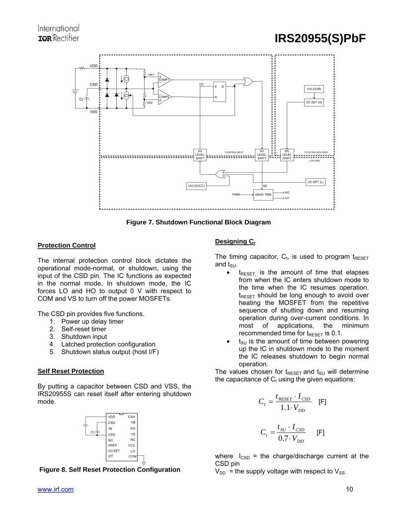
Figure 7. Shutdown Functional Block Diagram
Protection Control The internal protection control block dictates the operational mode-normal, or shutdown, using the input of the CSD pin. The IC functions as expected in the normal mode. In shutdown mode, the IC forces LO and HO to output 0 V with respect to COM and VS to turn off the power MOSFETs. The CSD pin provides five functions.
1. Power up delay timer 2. Self-reset timer 3. Shutdown input 4. Latched protection configuration 5. Shutdown status output (host I/F)
Self Reset Protection By putting a capacitor between CSD and VSS, the IRS20955S can reset itself after entering shutdown mode.
VB
VDD
IN
CSD
VSS
COM
OCSET LO
VCC
HO
VS
DT
CSH
NCNCVREF
Ct
Figure 8. Self Reset Protection Configuration
Designing Ct The timing capacitor, Ct, is used to program tRESET and tSU.
• tRESET, is the amount of time that elapses from when the IC enters shutdown mode to the time when the IC resumes operation. tRESET should be long enough to avoid over heating the MOSFET from the repetitive sequence of shutting down and resuming operation during over-current conditions. In most of applications, the minimum recommended time for tRESET is 0.1.
• tSU is the amount of time between powering up the IC in shutdown mode to the moment the IC releases shutdown to begin normal operation.
The values chosen for tRESET and tSU will determine the capacitance of Ct using the given equations:
DD
CSDRESETt V
ItC
⋅⋅
=1.1
[F]
DD
CSDSUt V
ItC
⋅⋅
=7.0
[F]
where ICSD = the charge/discharge current at the CSD pin VDD = the supply voltage with respect to VSS.
IRS20955(S)PbF
www.irf.com 11
Shutdown Input When VCSD falls below Vth2, the IRS20955S begins to charge Ct in an attempt to resume operation. Once the voltage of the CSD pin rises above the upper threshold, Vth1, the IC begins to operate normally again.
SHUTDOWN
VB
VDD
IN
CSD
VSS
COM
OCSET LO
VCC
HO
VS
DT
CSH
NCNCVREF
Figure 9. Shutdown Input
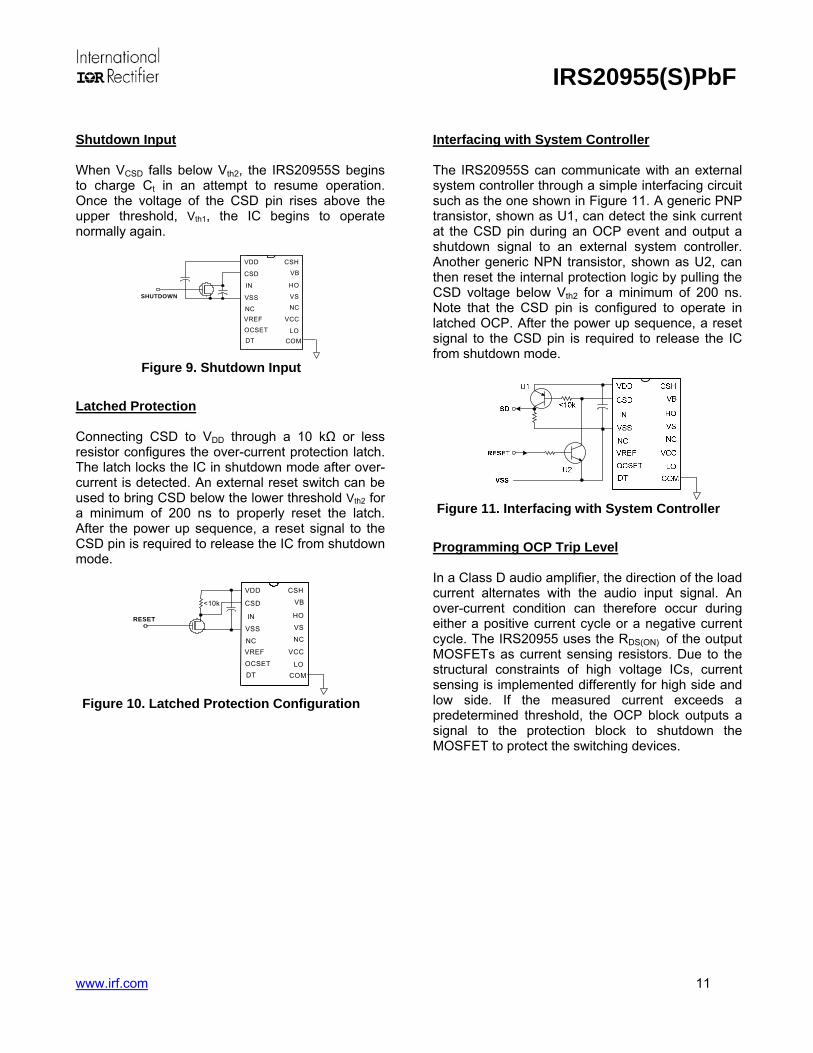
Latched Protection Connecting CSD to VDD through a 10 kΩ or less resistor configures the over-current protection latch. The latch locks the IC in shutdown mode after over-current is detected. An external reset switch can be used to bring CSD below the lower threshold Vth2 for a minimum of 200 ns to properly reset the latch. After the power up sequence, a reset signal to the CSD pin is required to release the IC from shutdown mode.
VB
VDD
IN
CSD
VSS
COM
OCSET LO
VCC
HO
VS
DT
CSH
NCNCVREF
<10k
RESET
Figure 10. Latched Protection Configuration
Interfacing with System Controller The IRS20955S can communicate with an external system controller through a simple interfacing circuit such as the one shown in Figure 11. A generic PNP transistor, shown as U1, can detect the sink current at the CSD pin during an OCP event and output a shutdown signal to an external system controller. Another generic NPN transistor, shown as U2, can then reset the internal protection logic by pulling the CSD voltage below Vth2 for a minimum of 200 ns. Note that the CSD pin is configured to operate in latched OCP. After the power up sequence, a reset signal to the CSD pin is required to release the IC from shutdown mode.
Figure 11. Interfacing with System Controller
Programming OCP Trip Level In a Class D audio amplifier, the direction of the load current alternates with the audio input signal. An over-current condition can therefore occur during either a positive current cycle or a negative current cycle. The IRS20955 uses the RDS(ON) of the output MOSFETs as current sensing resistors. Due to the structural constraints of high voltage ICs, current sensing is implemented differently for high side and low side. If the measured current exceeds a predetermined threshold, the OCP block outputs a signal to the protection block to shutdown the MOSFET to protect the switching devices.
IRS20955(S)PbF
www.irf.com 12
HIGH SIDE CS
VB
HO
VS
LOW SIDE CS
UV Q
UV DETECT
DEAD TIME
VCC
LO
COM
CSH
SD
OCSET
UV DETECT
HVLEVEL SHIFT
HVLEVEL SHIFT
FLOATING HIGH SIDE
5V REG
-B
Vcc
+B
OUT
R1
R2
R3
D1
Q1
Q2
R4
R5
Dbs
Cbs
VREF
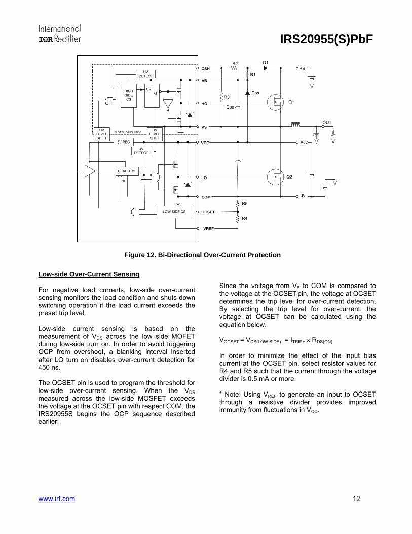
Figure 12. Bi-Directional Over-Current Protection
Low-side Over-Current Sensing For negative load currents, low-side over-current sensing monitors the load condition and shuts down switching operation if the load current exceeds the preset trip level. Low-side current sensing is based on the measurement of VDS across the low side MOFET during low-side turn on. In order to avoid triggering OCP from overshoot, a blanking interval inserted after LO turn on disables over-current detection for 450 ns. The OCSET pin is used to program the threshold for low-side over-current sensing. When the VDS measured across the low-side MOSFET exceeds the voltage at the OCSET pin with respect COM, the IRS20955S begins the OCP sequence described earlier.
Since the voltage from VS to COM is compared to the voltage at the OCSET pin, the voltage at OCSET determines the trip level for over-current detection. By selecting the trip level for over-current, the voltage at OCSET can be calculated using the equation below. VOCSET = VDS(LOW SIDE) = ITRIP+ x RDS(ON) In order to minimize the effect of the input bias current at the OCSET pin, select resistor values for R4 and R5 such that the current through the voltage divider is 0.5 mA or more. * Note: Using VREF to generate an input to OCSET through a resistive divider provides improved immunity from fluctuations in VCC.
IRS20955(S)PbF
www.irf.com 13
OC REF
OCREF
COM
OCSET
VS
OC+-
IRS20955
OC Comparator
R4
R5
-B
+B
OUT
Q1
Q2LOLO
0.5mA5.1V
Figure 13. Low-Side Over-Current Sensing
Low-Side Over-Current Setting Let the low-side MOSFET have an RDS(ON) of 100 mΩ and set the current trip level to 30 A. VOCSET is given by: VOCSET = ITRIP+ x RDS(ON) = 30 A x 100 mΩ = 3.0 V Choose R4+R5=10 kΩ to properly load the VREF pin.
Ω=
Ω⋅=
Ω⋅=
k
kVV
kV
VRREF
OCSET
8.5
101.50.3
105
where VREF = 5.1 V Based on the E-12 series of resistor values, choose R5 to be 5.6 kΩ and R4 to be 3.9 kΩ to complete the design. In general, RDS(ON) has a positive temperature coefficient that needs to be considered when setting the threshold level. Variations in RDS(ON) will affect the selection of external or internal component values.
High-Side Over-Current Sensing For positive load currents, high-side over-current sensing also monitors the load condition and shuts down the switching operation if the load current exceeds the preset trip level.
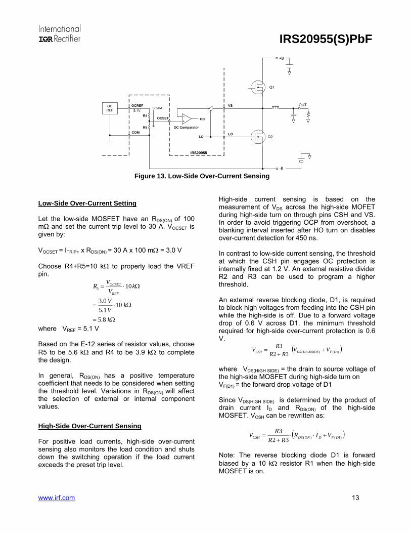
High-side current sensing is based on the measurement of VDS across the high-side MOFET during high-side turn on through pins CSH and VS. In order to avoid triggering OCP from overshoot, a blanking interval inserted after HO turn on disables over-current detection for 450 ns. In contrast to low-side current sensing, the threshold at which the CSH pin engages OC protection is internally fixed at 1.2 V. An external resistive divider R2 and R3 can be used to program a higher threshold. An external reverse blocking diode, D1, is required to block high voltages from feeding into the CSH pin while the high-side is off. Due to a forward voltage drop of 0.6 V across D1, the minimum threshold required for high-side over-current protection is 0.6 V.
( ))1()(323
DFHIGHSIDEDSCSH VVRR
RV +⋅+
=
where VDS(HIGH SIDE) = the drain to source voltage of the high-side MOSFET during high-side turn on VF(D1) = the forward drop voltage of D1 Since VDS(HIGH SIDE) is determined by the product of drain current ID and RDS(ON) of the high-side MOSFET. VCSH can be rewritten as:
( ))1()(323
DFDONDSCSH VIRRR
RV +⋅⋅+
=
Note: The reverse blocking diode D1 is forward biased by a 10 kΩ resistor R1 when the high-side MOSFET is on.
IRS20955(S)PbF
www.irf.com 14
VS
OC +-
IRS20955
CSH Comparator
-B
+B
OUT
Q1
Q2
HO
LO
HO
R1
R2
R3
D1
VB
CSH
Vcc
1.2V
Figure 14. Programming High-Side Over-Current Threshold
High-Side Over-Current Setting Figure 14 demonstrates the typical circuitry used for high-side current sensing. In the following example, the over-current protection level is set to trip at 30 A using a MOSFET with an RDS(ON) of 100 mΩ. The component values of R2 and R3 can be calculated using the following formula: Let R2 + R3=10 kΩ.
FDS
OCH
VVVthkR
+⋅Ω= 103
where Vth,OCL = 1.2 V VF = the forward voltage of reverse blocking
diode D1 = 0.6 V.
VDS@ID=30A = the voltage drop across the high-side MOSFET when the MOSFET current is 30 A. Therefore, VDS@ID=30A = ID x RDS(ON) = 30 A x 100 mΩ = 3 V Based on the formulas above, R2 = 6.8 kΩ and R3 = 3.3 kΩ. Choosing the Right Reverse Blocking Diode The selection of the appropriate reverse blocking diode used in place of D1 depends on its voltage rating and speed. To effectively block bus voltages, the reverse voltage must be higher than the voltage difference between +B and -B and the reverse recovery time must be as fast as the boot strap charging diode. A diode such as the Philips BAV21
W, a 200 V, 50 ns high speed switching diode, is more than sufficient.
Deadtime Generator Deadtime is a blanking period inserted between high-side turn on and low-side turn on to prevent shoot through. In the IRS20955S, an internal dead-time generation block allows the user to select the optimum deadtime from a range of preset values. Selecting a preset deadtime through the DT/SD pin voltage can easily be done through an external voltage divider. This way of setting deadtime prevents outside noise from modulating the switching timing, which is critical to the audio performances.
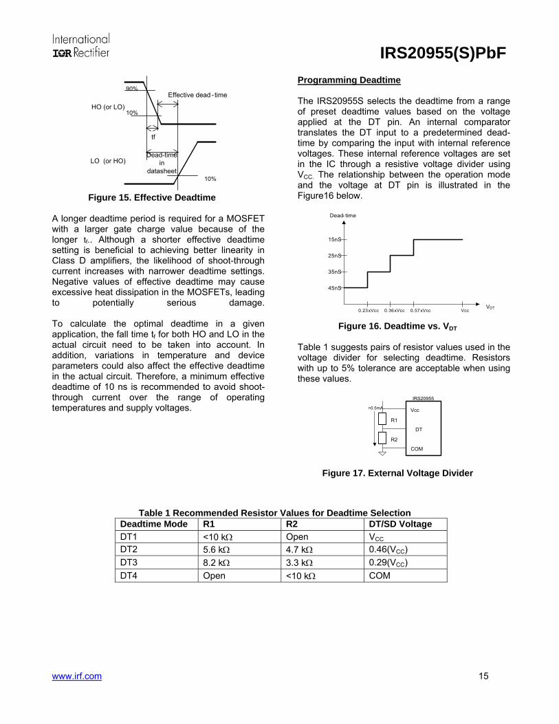
How to Determine Optimal Deadtime The effective deadtime in an actual application differs from the deadtime specified in this datasheet due to the switching fall time, tf.. The deadtime value in this datasheet is defined as the time period between the beginning of turn-off on one side of the switching stage and the beginning of turn-on on the other side as shown in Figure 15. The fall time of MOSFET gate voltage must be subtracted from the deadtime value in the datasheet to determine the effective deadtime of a Class D audio amplifier. (Effective deadtime) = (Deadtime in datasheet) – tf.
IRS20955(S)PbF
www.irf.com 15
HO (or LO)
LO (or HO)
tf
Dead-time in
datasheet
Effective dead -time
10%
10%
90%
Figure 15. Effective Deadtime
A longer deadtime period is required for a MOSFET with a larger gate charge value because of the longer tf.. Although a shorter effective deadtime setting is beneficial to achieving better linearity in Class D amplifiers, the likelihood of shoot-through current increases with narrower deadtime settings. Negative values of effective deadtime may cause excessive heat dissipation in the MOSFETs, leading to potentially serious damage. To calculate the optimal deadtime in a given application, the fall time tf for both HO and LO in the actual circuit need to be taken into account. In addition, variations in temperature and device parameters could also affect the effective deadtime in the actual circuit. Therefore, a minimum effective deadtime of 10 ns is recommended to avoid shoot-through current over the range of operating temperatures and supply voltages.
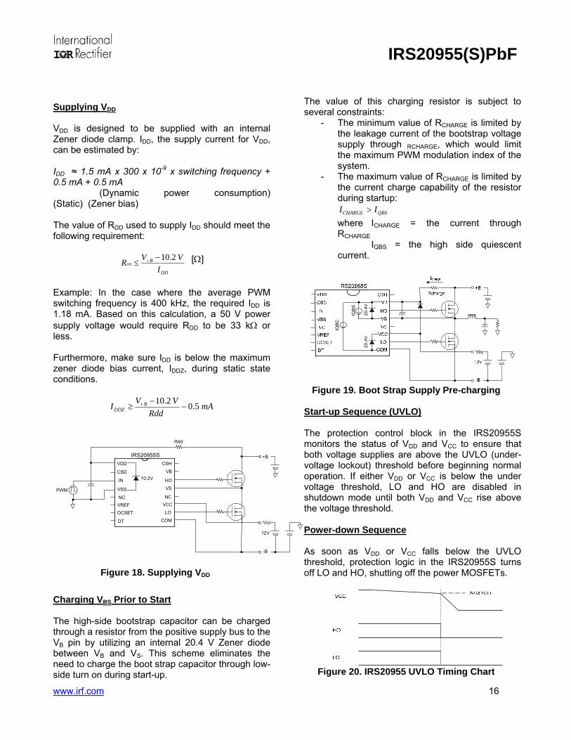
Programming Deadtime The IRS20955S selects the deadtime from a range of preset deadtime values based on the voltage applied at the DT pin. An internal comparator translates the DT input to a predetermined dead-time by comparing the input with internal reference voltages. These internal reference voltages are set in the IC through a resistive voltage divider using VCC. The relationship between the operation mode and the voltage at DT pin is illustrated in the Figure16 below.
Vcc 0.57xVcc 0.36xVcc 0.23xVcc
45nS
35nS
25nS
15nS
VDT
Dead- time
Figure 16. Deadtime vs. VDT
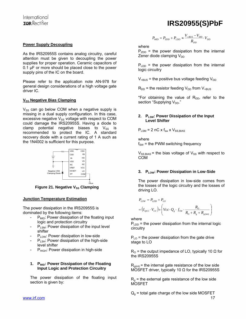
Table 1 suggests pairs of resistor values used in the voltage divider for selecting deadtime. Resistors with up to 5% tolerance are acceptable when using these values.
Vcc
COM
DT
>0.5mA
R1
R2
IRS20955
Figure 17. External Voltage Divider
Table 1 Recommended Resistor Values for Deadtime Selection Deadtime Mode R1 R2 DT/SD Voltage DT1 <10 kΩ Open VCC DT2 5.6 kΩ 4.7 kΩ 0.46(VCC) DT3 8.2 kΩ 3.3 kΩ 0.29(VCC) DT4 Open <10 kΩ COM
IRS20955(S)PbF
www.irf.com 16
Supplying VDD VDD is designed to be supplied with an internal Zener diode clamp. IDD, the supply current for VDD, can be estimated by: IDD ≈ 1.5 mA x 300 x 10-9 x switching frequency + 0.5 mA + 0.5 mA
(Dynamic power consumption) (Static) (Zener bias) The value of RDD used to supply IDD should meet the following requirement:
DD
B
IVVRDD
2.10−≤ + [Ω]
Example: In the case where the average PWM switching frequency is 400 kHz, the required IDD is 1.18 mA. Based on this calculation, a 50 V power supply voltage would require RDD to be 33 kΩ or less. Furthermore, make sure IDD is below the maximum zener diode bias current, IDDZ, during static state conditions.
mARdd
VVI BDDZ 5.02.10
−−
≥ +
IRS20955S
12V
VDD
IN
CSD
VSS
COMOCSET LO
VCC
HO
VS
DT
CSH
VB
-B
Vcc
+B
PWM
VREFNC NC
10.2V
Rdd
Figure 18. Supplying VDD
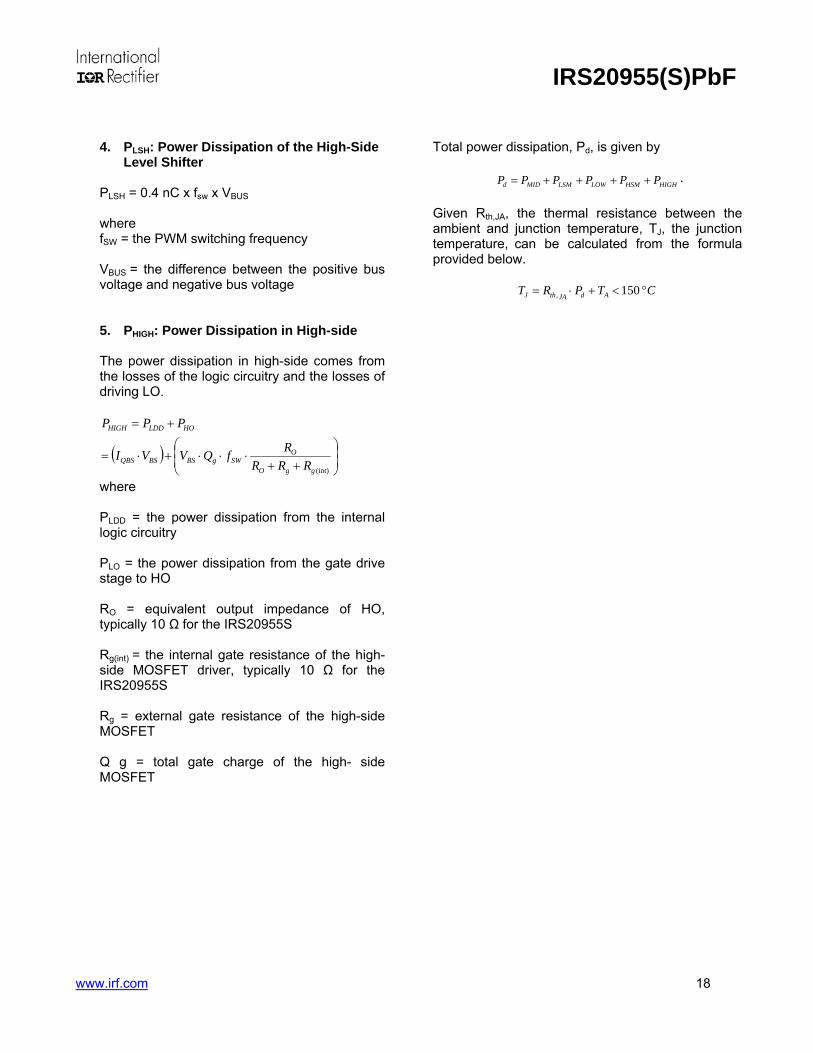
Charging VBS Prior to Start The high-side bootstrap capacitor can be charged through a resistor from the positive supply bus to the VB pin by utilizing an internal 20.4 V Zener diode between VB and VS. This scheme eliminates the need to charge the boot strap capacitor through low- side turn on during start-up.
The value of this charging resistor is subject to several constraints:
- The minimum value of RCHARGE is limited by the leakage current of the bootstrap voltage supply through RCHARGE, which would limit the maximum PWM modulation index of the system.
- The maximum value of RCHARGE is limited by the current charge capability of the resistor during startup:
QBSCHARGE II > where ICHARGE = the current through RCHARGE
IQBS = the high side quiescent current.
20.4
V20
.4V
IQB
S
IQB
C
Figure 19. Boot Strap Supply Pre-charging
Start-up Sequence (UVLO) The protection control block in the IRS20955S monitors the status of VDD and VCC to ensure that both voltage supplies are above the UVLO (under- voltage lockout) threshold before beginning normal operation. If either VDD or VCC is below the under voltage threshold, LO and HO are disabled in shutdown mode until both VDD and VCC rise above the voltage threshold. Power-down Sequence As soon as VDD or VCC falls below the UVLO threshold, protection logic in the IRS20955S turns off LO and HO, shutting off the power MOSFETs.
Figure 20. IRS20955 UVLO Timing Chart
IRS20955(S)PbF
www.irf.com 17
Power Supply Decoupling As the IRS20955S contains analog circuitry, careful attention must be given to decoupling the power supplies for proper operation. Ceramic capacitors of 0.1 µF or more should be placed close to the power supply pins of the IC on the board. Please refer to the application note AN-978 for general design considerations of a high voltage gate driver IC. VSS Negative Bias Clamping VSS can go below COM when a negative supply is missing in a dual supply configuration. In this case, excessive negative VSS voltage with respect to COM could damage the IRS20955S. Having a diode to clamp potential negative biases to VSS is recommended to protect the IC. A standard recovery diode with a current rating of 1 A such as the 1N4002 is sufficient for this purpose.
VB
VDD
IN
CSD
VSS
COM
OCSET LO
VCC
HO
VS
DT
CSH
NCNCVREF
Negative VSS Clamping Diode
-Vbus Figure 21. Negative VSS Clamping
Junction Temperature Estimation The power dissipation in the IRS20955S is dominated by the following items:
- PMID: Power dissipation of the floating input logic and protection circuitry
- PLSM: Power dissipation of the input level shifter
- PLOW: Power dissipation in low-side - PLSH: Power dissipation of the high-side
level shifter - PHIGH: Power dissipation in high-side
1. PMID: Power Dissipation of the Floating Input Logic and Protection Circuitry
The power dissipation of the floating input section is given by:
DDDD
DDBUSLDDZDDMID V
RVVPPP ⋅
−≈+= +
where PZDD = the power dissipation from the internal Zener diode clamping VDD PLDD = the power dissipation from the internal logic circuitry V+BUS = the positive bus voltage feeding VDD RDD = the resistor feeding VDD from V+BUS *For obtaining the value of RDD, refer to the section “Supplying VDD.” 2. PLSM: Power Dissipation of the Input
Level Shifter
PLSM = 2 nC x fsw x VSS,BIAS where fSW = the PWM switching frequency VSS,BIAS = the bias voltage of VSS with respect to COM 3. PLOW: Power Dissipation in Low-Side The power dissipation in low-side comes from the losses of the logic circuitry and the losses of driving LO.
( ) ⎟⎟⎠
⎞⎜⎜⎝
⎛
++⋅⋅⋅+⋅=
+=
(int)ggO
OSWgCCQCC
LOLDDLOW
RRRRfQVccVI
PPP
where PLDD = the power dissipation from the internal logic circuitry PLO = the power dissipation from the gate drive stage to LO RO = the output impedance of LO, typically 10 Ω for the IRS20955S Rg(int) = the internal gate resistance of the low side MOSFET driver, typically 10 Ω for the IRS20955S Rg = the external gate resistance of the low side MOSFET Qg = total gate charge of the low side MOSFET
IRS20955(S)PbF
www.irf.com 18
4. PLSH: Power Dissipation of the High-Side
Level Shifter
PLSH = 0.4 nC x fsw x VBUS where fSW = the PWM switching frequency VBUS = the difference between the positive bus voltage and negative bus voltage 5. PHIGH: Power Dissipation in High-side The power dissipation in high-side comes from the losses of the logic circuitry and the losses of driving LO.
( ) ⎟⎟⎠
⎞⎜⎜⎝
⎛
++⋅⋅⋅+⋅=
+=
(int)ggO
OSWgBSBSQBS
HOLDDHIGH
RRRRfQVVI
PPP
where PLDD = the power dissipation from the internal logic circuitry PLO = the power dissipation from the gate drive stage to HO RO = equivalent output impedance of HO, typically 10 Ω for the IRS20955S Rg(int) = the internal gate resistance of the high-side MOSFET driver, typically 10 Ω for the IRS20955S Rg = external gate resistance of the high-side MOSFET Q g = total gate charge of the high- side MOSFET
Total power dissipation, Pd, is given by
HIGHHSMLOWLSMMIDd PPPPPP ++++= . Given Rth,JA, the thermal resistance between the ambient and junction temperature, TJ, the junction temperature, can be calculated from the formula provided below.
CTPRT AdJAthJ °<+⋅= 150,
IRS20955(S)PbF
www.irf.com 19
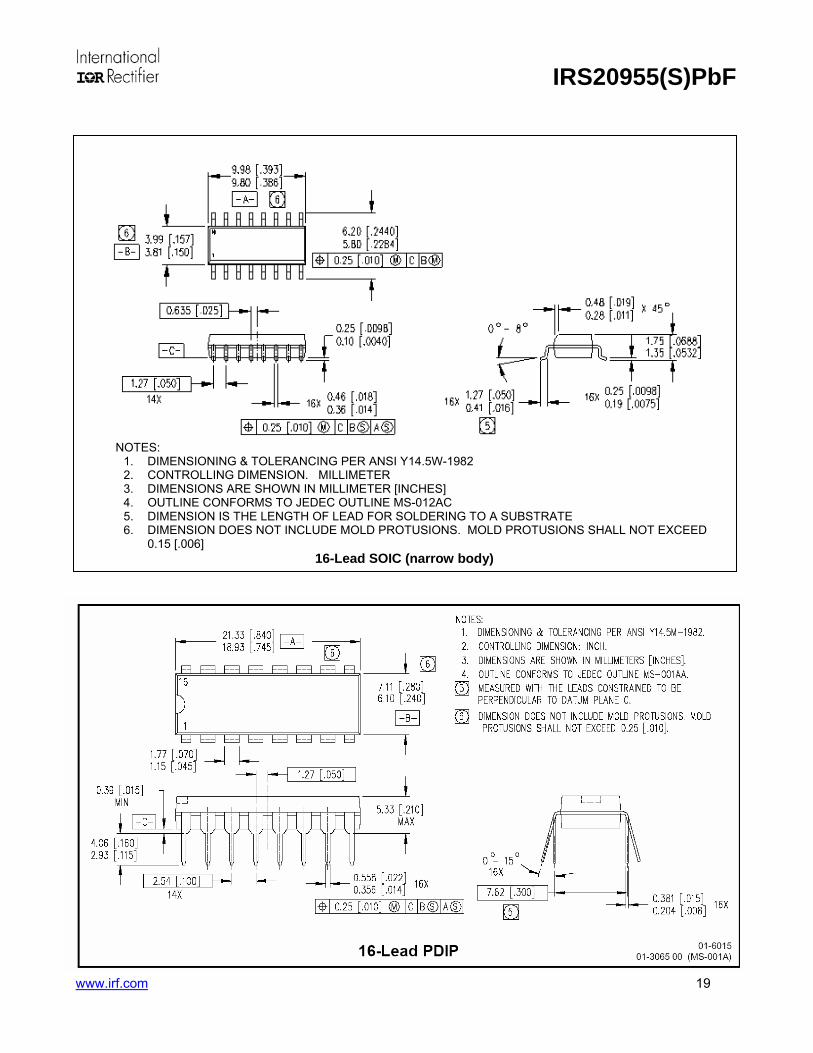
NOTES: 1. DIMENSIONING & TOLERANCING PER ANSI Y14.5W-1982 2. CONTROLLING DIMENSION. MILLIMETER 3. DIMENSIONS ARE SHOWN IN MILLIMETER [INCHES] 4. OUTLINE CONFORMS TO JEDEC OUTLINE MS-012AC 5. DIMENSION IS THE LENGTH OF LEAD FOR SOLDERING TO A SUBSTRATE 6. DIMENSION DOES NOT INCLUDE MOLD PROTUSIONS. MOLD PROTUSIONS SHALL NOT EXCEED
0.15 [.006] 16-Lead SOIC (narrow body)
IRS20955(S)PbF
www.irf.com 20
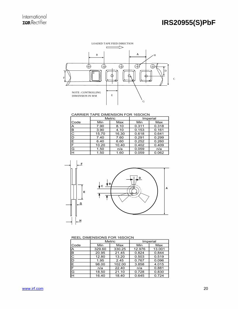
CARRIER TAPE DIMENSION FOR 16SOICN
Code Min Max Min MaxA 7.90 8.10 0.311 0.318B 3.90 4.10 0.153 0.161C 15.70 16.30 0.618 0.641D 7.40 7.60 0.291 0.299E 6.40 6.60 0.252 0.260F 10.20 10.40 0.402 0.409G 1.50 n/a 0.059 n/aH 1.50 1.60 0.059 0.062
Metric Imperial
REEL DIMENSIONS FOR 16SOICN
Code Min Max Min MaxA 329.60 330.25 12.976 13.001B 20.95 21.45 0.824 0.844C 12.80 13.20 0.503 0.519D 1.95 2.45 0.767 0.096E 98.00 102.00 3.858 4.015F n/a 22.40 n/a 0.881G 18.50 21.10 0.728 0.830H 16.40 18.40 0.645 0.724
Metric Imperial
E
F
A
C
D
G
AB H
NOTE : CONTROLLING DIMENSION IN MM
LOADED TAPE FEED DIRECTION
A
H
F
E
G
D
BC
IRS20955(S)PbF
www.irf.com 21
SO-16 package is MSL3 qualified.
This product has been designed and qualified for the industrial level. Qualification standards can be found at IR’s Web Site http://www.irf.com/
WORLD HEADQUARTERS: 233 Kansas St., El Segundo, California 90245 Tel: (310) 252-7105 Data and specifications subject to change without notice 08/02/2007
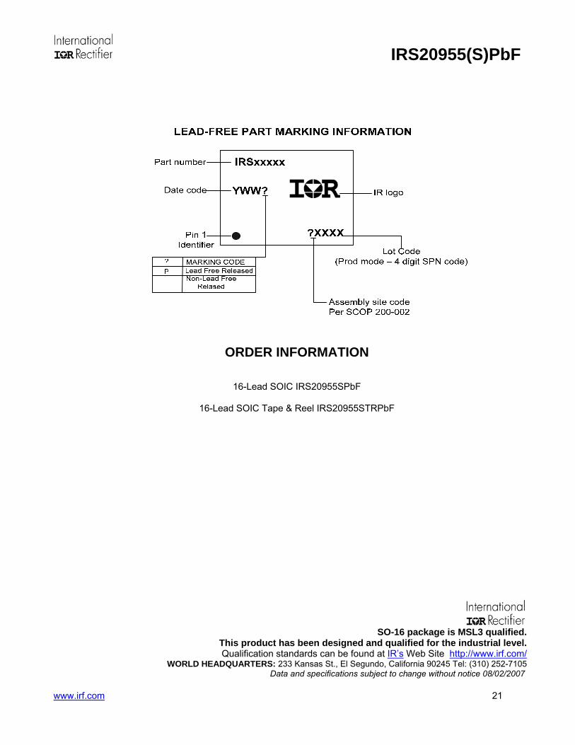
ORDER INFORMATION
16-Lead SOIC IRS20955SPbF
16-Lead SOIC Tape & Reel IRS20955STRPbF