Embed Size (px)
Citation preview
IREAP
Studies of HPM Effects in Electronic Systems
J. Rodgers, M. Holloway (DEPS Scholar), T. Firestone andV. L. Granatstein,
Institute for Research in Electronics and Applied PhysicsUniversity of Maryland
College Park, MD 20742
IREAP
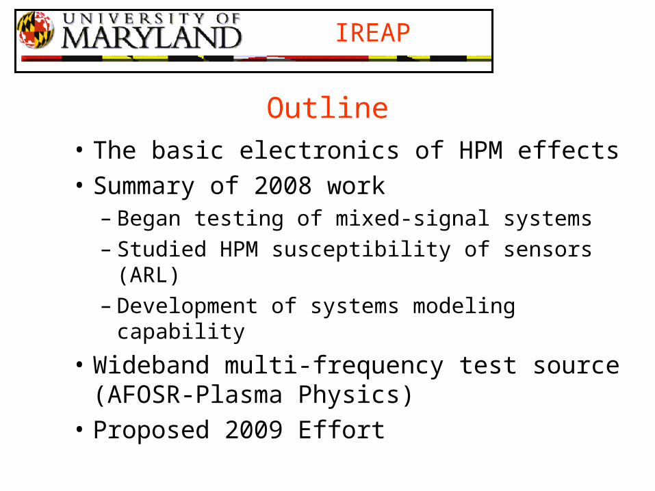
Outline
• The basic electronics of HPM effects
• Summary of 2008 work– Began testing of mixed-signal systems– Studied HPM susceptibility of sensors (ARL)– Development of systems modeling capability
• Wideband multi-frequency test source (AFOSR-Plasma Physics)
• Proposed 2009 Effort
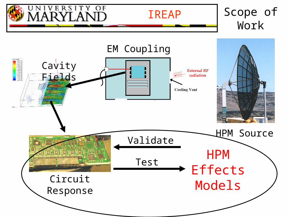
IREAP Scope of Work
HPM Source
EM Coupling
Cavity Fields
Circuit Response
HPM Effects Models
Test
Validate
IREAP
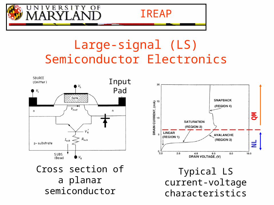
Large-signal (LS) Semiconductor Electronics
Typical LS current-voltage characteristics
Input Pad
Cross section of a planar semiconductor
QM
NL
IREAP
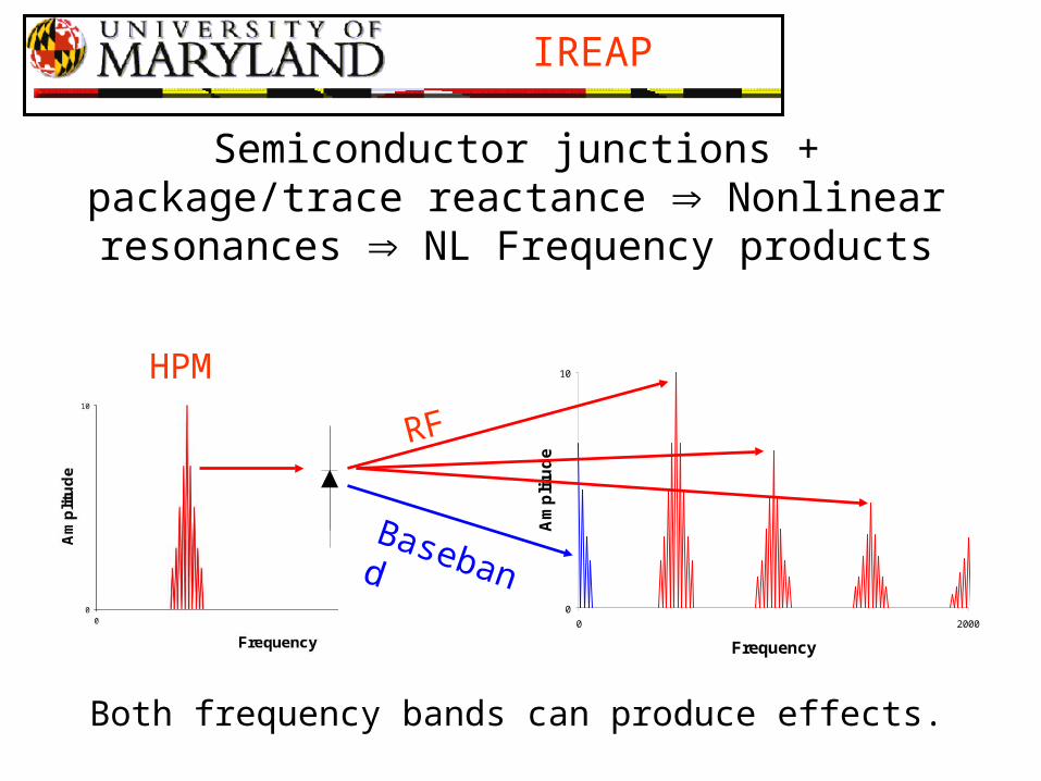
Semiconductor junctions + package/trace reactance Nonlinear resonances NL Frequency products
0
10
0 2000
Frequency
Am
pli
tud
eBaseband
RF
Both frequency bands can produce effects.
HPM
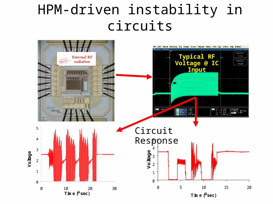
HPM-driven instability in circuits
Typical RF Voltage @ IC Input
0
1
2
3
4
5
0 10 20 30Time (msec)
Vo
ltag
e
Circuit Response
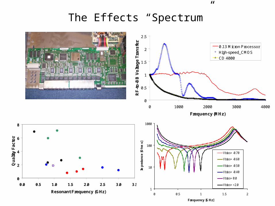
The Effects “Spectrum”
0
2
4
6
8
0.0 0.5 1.0 1.5 2.0 2.5 3.0 3.5
Resonant Frequency (GHz)
Qu
ali
ty F
ac
tor
0
0.5
1
1.5
2
2.5
0 1000 2000 3000 4000
Frequency (MHz)
RF
-to
-BB
Vo
lta
ge
Tra
ns
fer
0.13 Micron Processor
High-speed_CMOS
CD 4000
IREAP
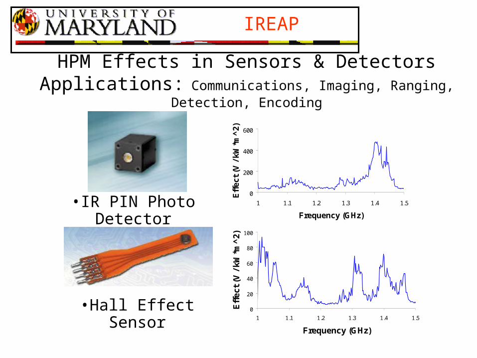
HPM Effects in Sensors & DetectorsApplications: Communications, Imaging, Ranging, Detection, Encoding
0
200
400
600
1 1.1 1.2 1.3 1.4 1.5
Frequency (GHz)
Eff
ec
t (V
/ k
W*m
^2
)
0
20
40
60
80
100
1 1.1 1.2 1.3 1.4 1.5
Frequency (GHz)
Eff
ec
t (V
/ k
W*m
^2
)
•IR PIN Photo Detector
•Hall Effect Sensor
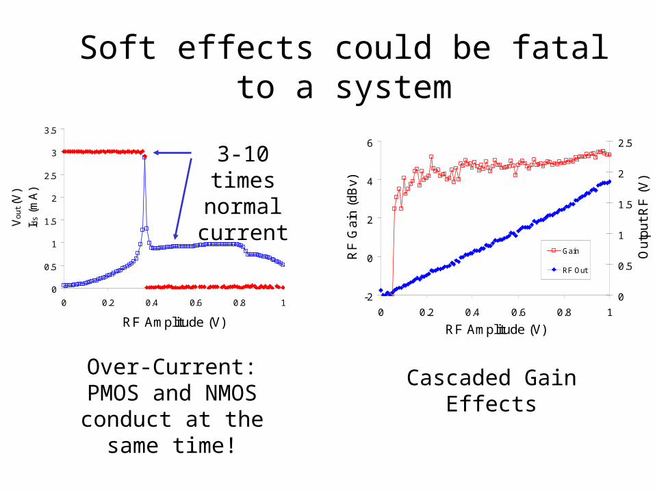
Soft effects could be fatal to a system
Over-Current: PMOS and NMOS conduct at
the same time!
Cascaded Gain Effects
0
0.5
1
1.5
2
2.5
3
3.5
0 0.2 0.4 0.6 0.8 1
RF Amplitude (V)
Vo
ut (
V)
I ds
(mA
)
-2
0
2
4
6
0 0.2 0.4 0.6 0.8 1
RF Amplitude (V)
RF
Gai
n (d
Bv)
0
0.5
1
1.5
2
2.5
Out
put
RF
(V
)
Gain
RF Out
3-10 times normal current
IREAP
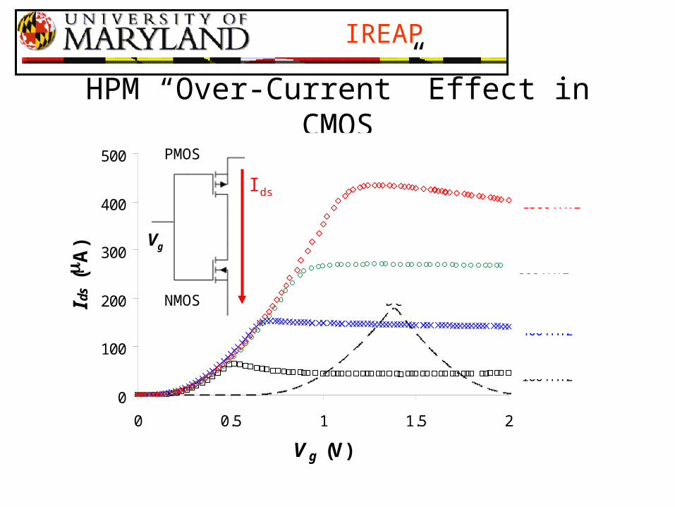
HPM “Over-Current” Effect in CMOS
0
100
200
300
400
500
0 0.5 1 1.5 2
V g (V)
I ds (m A
)
1500 MHz
800 MHz
400 MHz
100 MHz
DC
PMOS
NMOS
Ids
Vg
IREAP
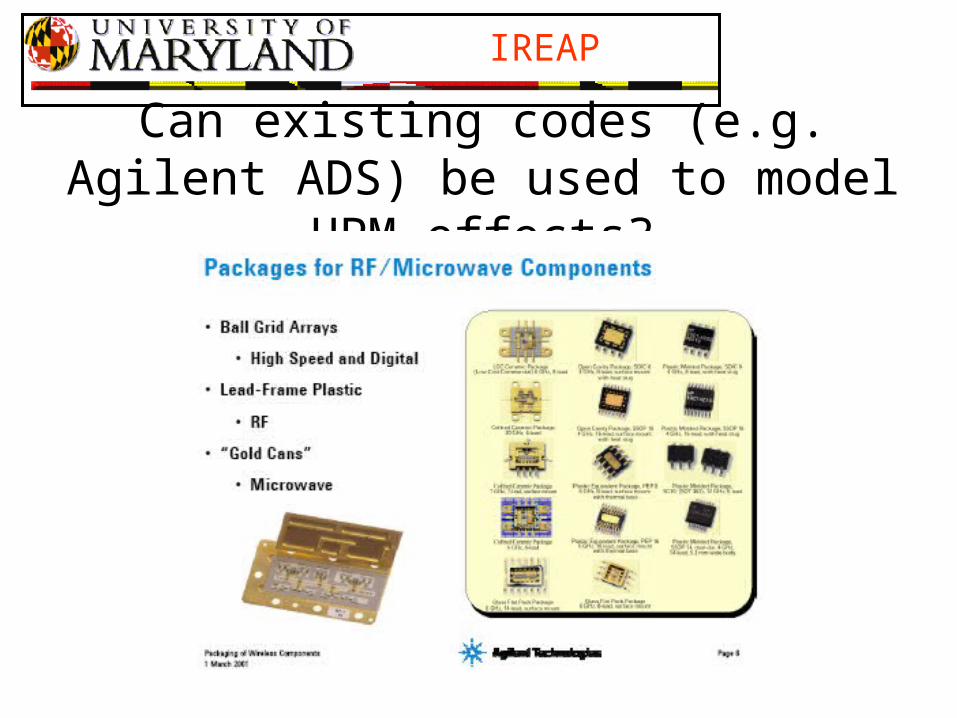
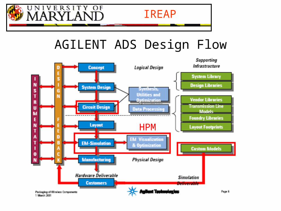
Can existing codes (e.g. Agilent ADS) be used to model HPM effects?
IREAP
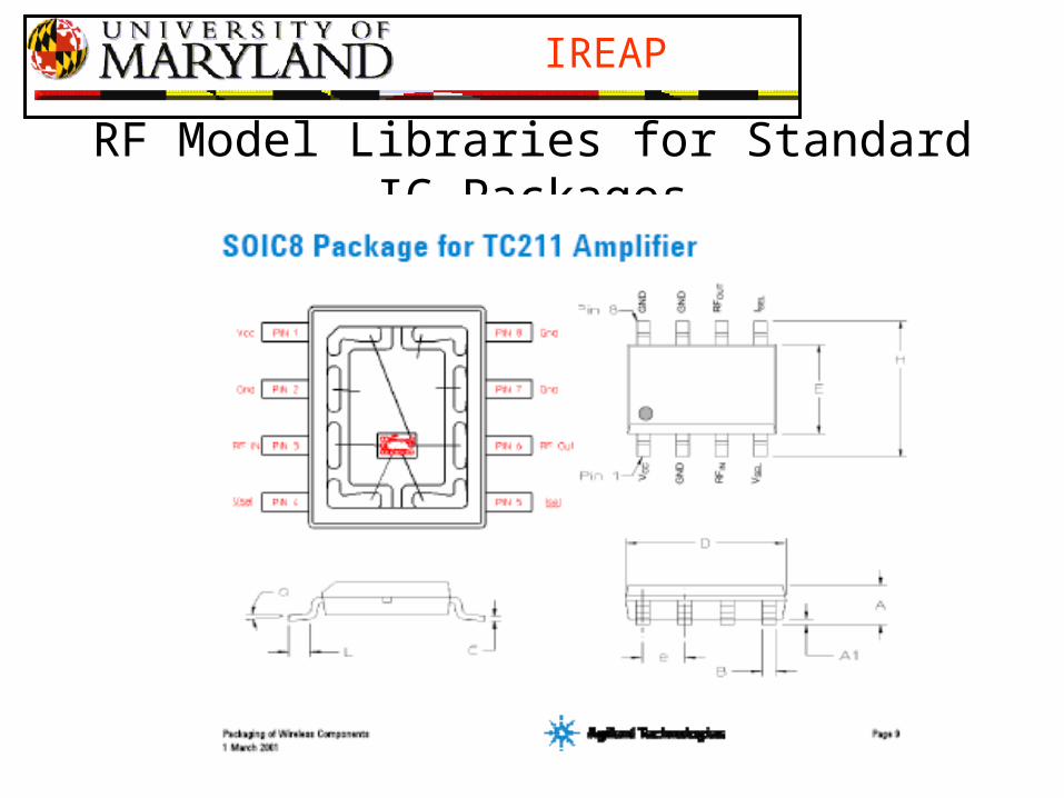
RF Model Libraries for Standard IC Packages
HPM
IREAP
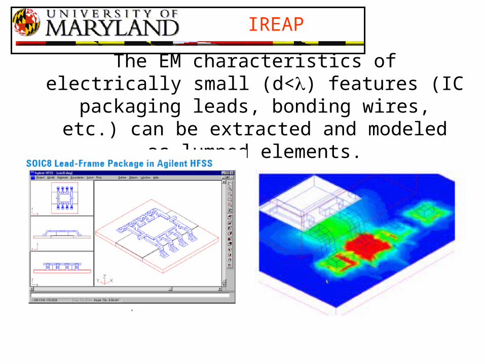
The EM characteristics of electrically small (d<) features (IC packaging leads, bonding wires, etc.) can
be extracted and modeled as lumped elements.
IREAP
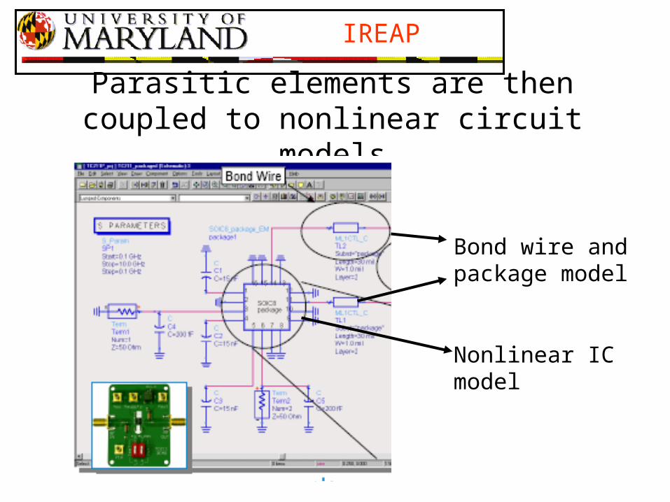
Parasitic elements are then coupled to nonlinear circuit models
Bond wire and package model
Nonlinear IC model
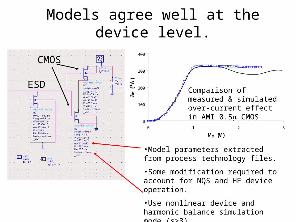
Models agree well at the device level.
0
100
200
300
400
0 1 2 3
V g (V)I d
s (m
A)
•Model parameters extracted from process technology files.
•Some modification required to account for NQS and HF device operation.
•Use nonlinear device and harmonic balance simulation mode (s>3).
Comparison of measured & simulated over-current effect in AMI 0.5m CMOS
CMOS
ESD
IREAP
AGILENT ADS Design Flow
HPM
IREAP
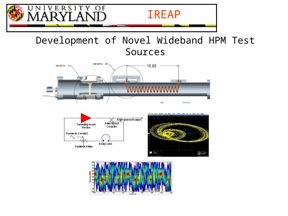
Development of Novel Wideband HPM Test Sources
High-Power RF Coupler
High-Current Plasma Cathode
E-BeamPlasma
DirectionalCoupler
Traveling-waveDevice
Variable Atten.Delay Line
High-power Output
Dynamic Control
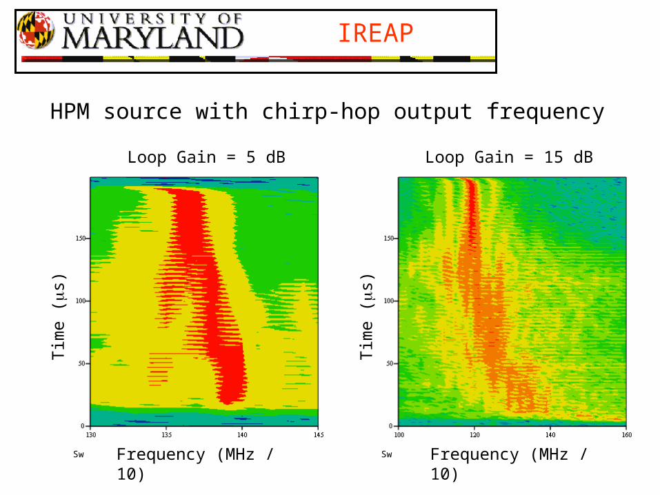
IREAP
Sw Frequency (MHz / 10)
Tim
e (m
s)
Loop Gain = 15 dB
Sw Frequency (MHz / 10)
Loop Gain = 5 dB
Tim
e (m
s)
HPM source with chirp-hop output frequency
IREAP
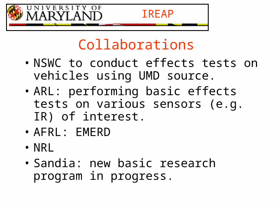
Collaborations• NSWC to conduct effects tests on vehicles
using UMD source.• ARL: performing basic effects tests on
various sensors (e.g. IR) of interest.• AFRL: EMERD• NRL• Sandia: new basic research program in
progress.

IREAP
Research Personnel• PhD:
– Todd Firestone, graduated December 2008– Mike Holloway, DEPS Scholarship, projected to
graduate fall 2009
• Postdoctoral:– Dr. Zeynep Dilli: QM device physics and
modeling, joined group Jan. 2009
• Undergraduates:– Collin Kennedy & Mark Strother (juniors physics)


![Logic Programming in ClojureDependency Graph Nodes (def doe (ref {:name “doe”:last-update (Date.):deps [rae fa sew]})) (def rae (ref {:name “rae”:last-update (Date.):deps [fa]}))](https://img.pdfslide.us/doc/110x75/5f775adacd82e475b70c7c10/logic-programming-in-clojure-dependency-graph-nodes-def-doe-ref-name-aoedoealast-update.jpg)