Embed Size (px)
Citation preview
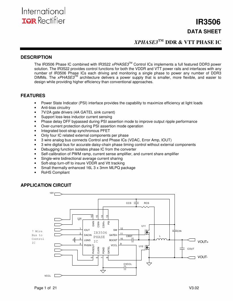
IR3506
Page 1 of 21 V3.02
DATA SHEET
XPHASE3TM
DDR & VTT PHASE IC
DESCRIPTION
The IR3506 Phase IC combined with IR3522 xPHASE3TM
Control ICs implements a full featured DDR3 power solution. The IR3522 provides control functions for both the VDDR and VTT power rails and interfaces with any number of IR3506 Phase ICs each driving and monitoring a single phase to power any number of DDR3 DIMMs. The xPHASE3
TM architecture delivers a power supply that is smaller, more flexible, and easier to
design while providing higher efficiency than conventional approaches.
FEATURES
• Power State Indicator (PSI) interface provides the capability to maximize efficiency at light loads
• Anti-bias circuitry
• 7V/2A gate drivers (4A GATEL sink current)
• Support loss-less inductor current sensing
• Phase delay DFF bypassed during PSI assertion mode to improve output ripple performance
• Over-current protection during PSI assertion mode operation
• Integrated boot-strap synchronous PFET
• Only four IC related external components per phase
• 3 wire analog bus connects Control and Phase ICs (VDAC, Error Amp, IOUT)
• 3 wire digital bus for accurate daisy-chain phase timing control without external components
• Debugging function isolates phase IC from the converter
• Self-calibration of PWM ramp, current sense amplifier, and current share amplifier
• Single-wire bidirectional average current sharing
• Soft-stop turn-off to insure VDDR and Vtt tracking
• Small thermally enhanced 16L 3 x 3mm MLPQ package
• RoHS Compliant
APPLICATION CIRCUIT
CCS
CVCCL
CS
IN-
15
PS
I13
EA
IN16
IOUT1
SW12
GATEH11
BOOST10
CS
IN+
14
DACIN2
CLK
IN6
PHSIN4
PH
SO
UT
5
GA
TE
L8
PG
ND
7
VCCL9
LGND3
IR3506
PHASE
IC
U1
CBST
RCS
U12
CIN
U11
L
VOUT-
VOUT+
12V
VCCL
7 Wire
Bus to
Control
IC
COUT
IR3506
Page 2 of 21 V3.02
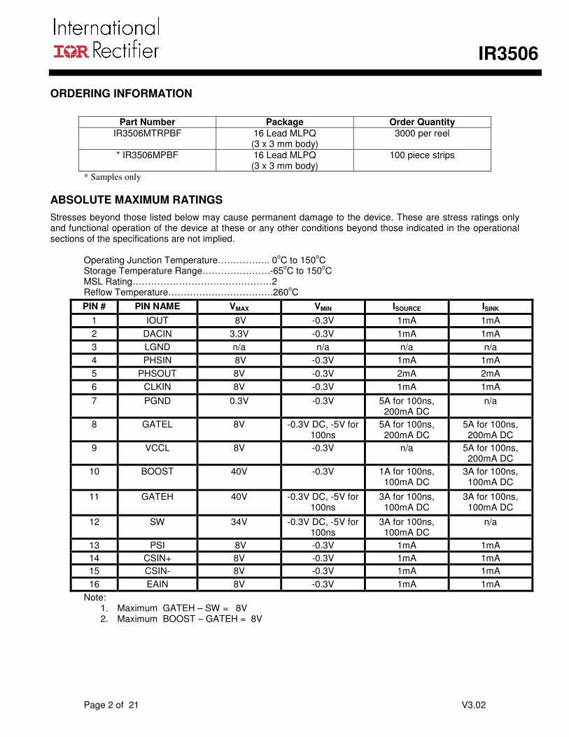
ORDERING INFORMATION
Part Number Package Order Quantity
IR3506MTRPBF 16 Lead MLPQ (3 x 3 mm body)
3000 per reel
* IR3506MPBF 16 Lead MLPQ (3 x 3 mm body)
100 piece strips
* Samples only
ABSOLUTE MAXIMUM RATINGS
Stresses beyond those listed below may cause permanent damage to the device. These are stress ratings only and functional operation of the device at these or any other conditions beyond those indicated in the operational sections of the specifications are not implied.
Operating Junction Temperature…………….. 0
oC to 150
oC
Storage Temperature Range………………….-65oC to 150
oC
MSL Rating………………………………………2 Reflow Temperature…………………………….260
oC
Note: 1. Maximum GATEH – SW = 8V 2. Maximum BOOST – GATEH = 8V
PIN # PIN NAME VMAX VMIN ISOURCE ISINK
1 IOUT 8V -0.3V 1mA 1mA
2 DACIN 3.3V -0.3V 1mA 1mA
3 LGND n/a n/a n/a n/a
4 PHSIN 8V -0.3V 1mA 1mA
5 PHSOUT 8V -0.3V 2mA 2mA
6 CLKIN 8V -0.3V 1mA 1mA
7 PGND 0.3V -0.3V 5A for 100ns, 200mA DC
n/a
8 GATEL 8V -0.3V DC, -5V for 100ns
5A for 100ns, 200mA DC
5A for 100ns, 200mA DC
9 VCCL 8V -0.3V n/a 5A for 100ns, 200mA DC
10 BOOST 40V -0.3V 1A for 100ns, 100mA DC
3A for 100ns, 100mA DC
11 GATEH 40V -0.3V DC, -5V for 100ns
3A for 100ns, 100mA DC
3A for 100ns, 100mA DC
12 SW 34V -0.3V DC, -5V for 100ns
3A for 100ns, 100mA DC
n/a
13 PSI 8V -0.3V 1mA 1mA
14 CSIN+ 8V -0.3V 1mA 1mA
15 CSIN- 8V -0.3V 1mA 1mA
16 EAIN 8V -0.3V 1mA 1mA

IR3506
Page 3 of 21 V3.02
RECOMMENDED OPERATING CONDITIONS FOR RELIABLE OPERATION WITH MARGIN
4.75V ≤ VCCL ≤ 7.5V, 0.5V ≤ V(DACIN) ≤ 1.6V, 250kHz ≤ CLKIN ≤ 9MHz, 250kHz ≤ PHSIN ≤1.5MHz, 0 oC ≤ TJ ≤
125 oC
ELECTRICAL CHARACTERISTICS
The electrical characteristics table list the spread of critical values that are guaranteed to be within the recommended operating conditions (unless otherwise specified). Typical values represent the median values, which are related to 25°C. CGATEH = 3.3nF, CGATEL = 6.8nF (unless otherwise specified).
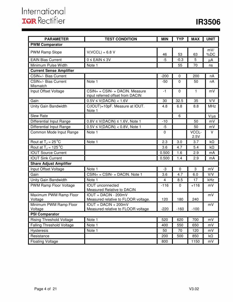
PARAMETER TEST CONDITION MIN TYP MAX UNIT
Gate Drivers
GATEH Source Resistance BOOST – SW = 7V. Note 1 1.0 2.5 Ω
GATEH Sink Resistance BOOST – SW = 7V. Note 1 1.0 2.5 Ω
GATEL Source Resistance VCCL – PGND = 7V. Note 1 1.0 2.5 Ω
GATEL Sink Resistance VCCL – PGND = 7V. Note 1 0.4 1.0 Ω
GATEH Source Current BOOST=7V, GATEH=2.5V, SW=0V. 2.0 A
GATEH Sink Current BOOST=7V, GATEH=2.5V, SW=0V. 2.0 A
GATEL Source Current VCCL=7V, GATEL=2.5V, PGND=0V. 2.0 A
GATEL Sink Current VCCL=7V, GATEL=2.5V, PGND=0V. 4.0 A
GATEH Rise Time BOOST – SW = 7V, measure 1V to 4V transition time
5 10 ns
GATEH Fall Time BOOST - SW = 7V, measure 4V to 1V transition time
5 10 ns
GATEL Rise Time VCCL – PGND = 7V, Measure 1V to 4V transition time
10 20 ns
GATEL Fall Time VCCL – PGND = 7V, Measure 4V to 1V transition time
5 10 ns
GATEL low to GATEH high delay
BOOST = VCCL = 7V, SW = PGND = 0V, measure time from GATEL falling to 1V to GATEH rising to 1V
10 20 40 ns
GATEH low to GATEL high delay
BOOST = VCCL = 7V, SW = PGND = 0V, measure time from GATEH falling to 1V to GATEL rising to 1V
10 20 40 ns
Disable Pull-Down Resistance
Note 1 30 80 130 kΩ
Clock
CLKIN Threshold Compare to V(VCCL) 45 %
CLKIN Bias Current CLKIN = V(VCCL) -0.5 0.0 0.5 µA
CLKIN Phase Delay Measure time from CLKIN<1V to GATEH>1V
40 75 125 ns
PHSIN Threshold Compare to V(VCCL) 35 50 55 %
PHSOUT Propagation Delay
Measure time from CLKIN > (VCCL * 50% ) to PHSOUT > (VCCL *50%). 10pF @125
oC
4 15 35 ns
PHSIN Pull-Down Resistance
30 100 170 kΩ
PHSOUT High Voltage I(PHSOUT) = -10mA, measure VCCL – PHSOUT
1 0.6 V
PHSOUT Low Voltage I(PHSOUT) = 10mA 0.4 1 V
IR3506
Page 4 of 21 V3.02
PARAMETER TEST CONDITION MIN TYP MAX UNIT
PWM Comparator
PWM Ramp Slope V(VCCL) = 6.8 V
46
53
63 mV/ %DC
EAIN Bias Current 0 ≤ EAIN ≤ 3V -5 -0.3 5 µA
Minimum Pulse Width Note 1 55 70 ns
Current Sense Amplifier
CSIN+/- Bias Current -200 0 200 nA
CSIN+/- Bias Current Mismatch
Note 1 -50 0 50 nA
Input Offset Voltage CSIN+ = CSIN- = DACIN. Measure input referred offset from DACIN
-1 0 1 mV
Gain 0.5V ≤ V(DACIN) < 1.6V 30 32.5 35 V/V
Unity Gain Bandwidth C(IOUT)=10pF. Measure at IOUT. Note 1
4.8 6.8 8.8 MHz
Slew Rate 6 V/µs
Differential Input Range 0.8V ≤ V(DACIN) ≤ 1.6V, Note 1 -10 50 mV
Differential Input Range 0.5V ≤ V(DACIN) < 0.8V, Note 1 -5 50 mV
Common Mode Input Range Note 1 0 VCCL-2.5V
V
Rout at TJ = 25 oC Note 1 2.3 3.0 3.7 kΩ
Rout at TJ = 125 oC 3.6 4.7 5.4 kΩ
IOUT Source Current 0.500 1.6 2.9 mA
IOUT Sink Current 0.500 1.4 2.9 mA
Share Adjust Amplifier
Input Offset Voltage Note 1 -3 0 3 mV
Gain CSIN+ = CSIN- = DACIN. Note 1 3.6 4.7 6.0 V/V
Unity Gain Bandwidth Note 1 4 8.5 17 kHz
PWM Ramp Floor Voltage IOUT unconnected Measured Relative to DACIN
-116 0 +116 mV
Maximum PWM Ramp Floor Voltage
IOUT = DACIN - 200mV Measured relative to FLOOR voltage.
120
180
240
mV
Minimum PWM Ramp Floor Voltage
IOUT = DACIN + 200mV Measured relative to FLOOR voltage
-220
-160
-100
mV
PSI Comparator
Rising Threshold Voltage Note 1 520 620 700 mV
Falling Threshold Voltage Note 1 400 550 650 mV
Hysteresis Note 1 50 70 120 mV
Resistance 200 500 850 kΩ
Floating Voltage 800 1150 mV
IR3506
Page 5 of 21 V3.02
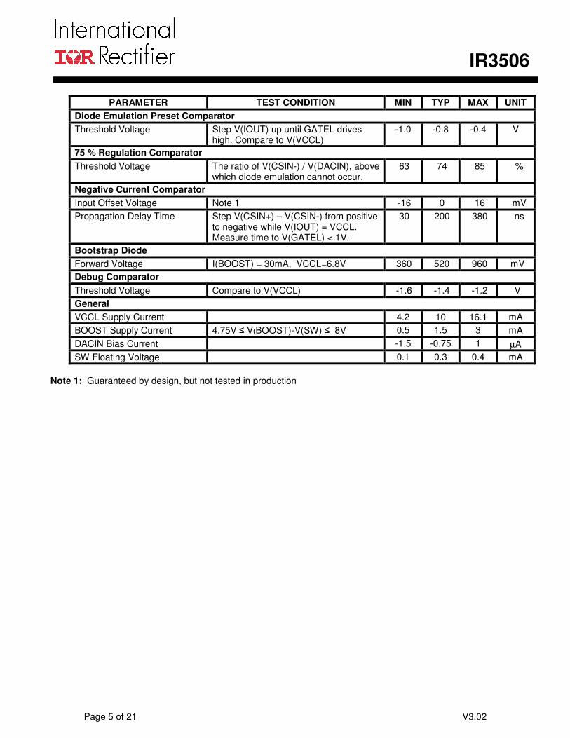
Note 1: Guaranteed by design, but not tested in production
PARAMETER TEST CONDITION MIN TYP MAX UNIT
Diode Emulation Preset Comparator
Threshold Voltage Step V(IOUT) up until GATEL drives high. Compare to V(VCCL)
-1.0 -0.8 -0.4 V
75 % Regulation Comparator
Threshold Voltage The ratio of V(CSIN-) / V(DACIN), above which diode emulation cannot occur.
63 74 85 %
Negative Current Comparator
Input Offset Voltage Note 1 -16 0 16 mV
Propagation Delay Time Step V(CSIN+) – V(CSIN-) from positive to negative while V(IOUT) = VCCL. Measure time to V(GATEL) < 1V.
30 200 380 ns
Bootstrap Diode
Forward Voltage I(BOOST) = 30mA, VCCL=6.8V 360 520 960 mV
Debug Comparator
Threshold Voltage Compare to V(VCCL) -1.6 -1.4 -1.2 V
General
VCCL Supply Current 4.2 10 16.1 mA
BOOST Supply Current 4.75V ≤ V(BOOST)-V(SW) ≤ 8V 0.5 1.5 3 mA
DACIN Bias Current -1.5 -0.75 1 µA
SW Floating Voltage 0.1 0.3 0.4 mA
IR3506
Page 6 of 21 V3.02
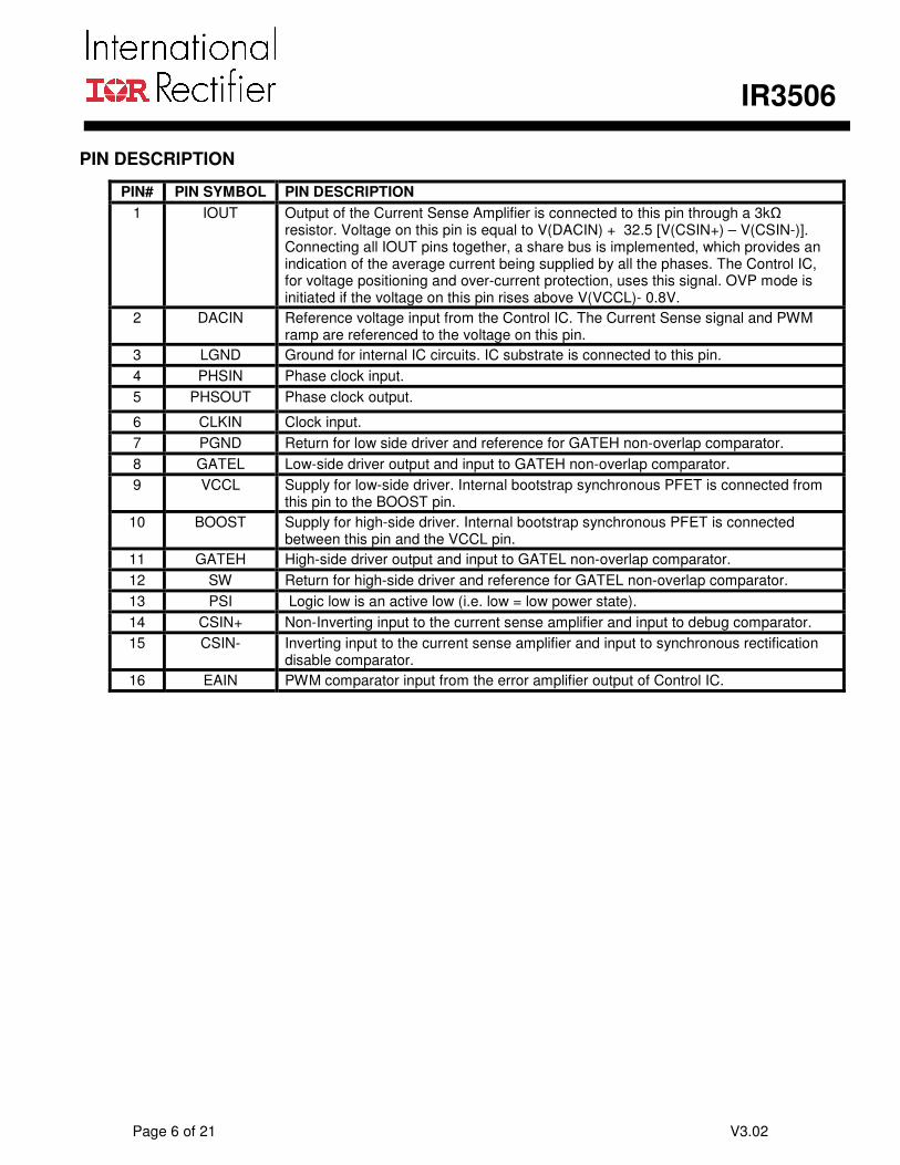
PIN DESCRIPTION
PIN# PIN SYMBOL PIN DESCRIPTION
1 IOUT Output of the Current Sense Amplifier is connected to this pin through a 3kΩ resistor. Voltage on this pin is equal to V(DACIN) + 32.5 [V(CSIN+) – V(CSIN-)]. Connecting all IOUT pins together, a share bus is implemented, which provides an indication of the average current being supplied by all the phases. The Control IC, for voltage positioning and over-current protection, uses this signal. OVP mode is initiated if the voltage on this pin rises above V(VCCL)- 0.8V.
2 DACIN Reference voltage input from the Control IC. The Current Sense signal and PWM ramp are referenced to the voltage on this pin.
3 LGND Ground for internal IC circuits. IC substrate is connected to this pin.
4 PHSIN Phase clock input.
5 PHSOUT Phase clock output.
6 CLKIN Clock input.
7 PGND Return for low side driver and reference for GATEH non-overlap comparator.
8 GATEL Low-side driver output and input to GATEH non-overlap comparator.
9 VCCL Supply for low-side driver. Internal bootstrap synchronous PFET is connected from this pin to the BOOST pin.
10 BOOST Supply for high-side driver. Internal bootstrap synchronous PFET is connected between this pin and the VCCL pin.
11 GATEH High-side driver output and input to GATEL non-overlap comparator.
12 SW Return for high-side driver and reference for GATEL non-overlap comparator.
13 PSI Logic low is an active low (i.e. low = low power state).
14 CSIN+ Non-Inverting input to the current sense amplifier and input to debug comparator.
15 CSIN- Inverting input to the current sense amplifier and input to synchronous rectification disable comparator.
16 EAIN PWM comparator input from the error amplifier output of Control IC.
IR3506
Page 7 of 21 V3.02
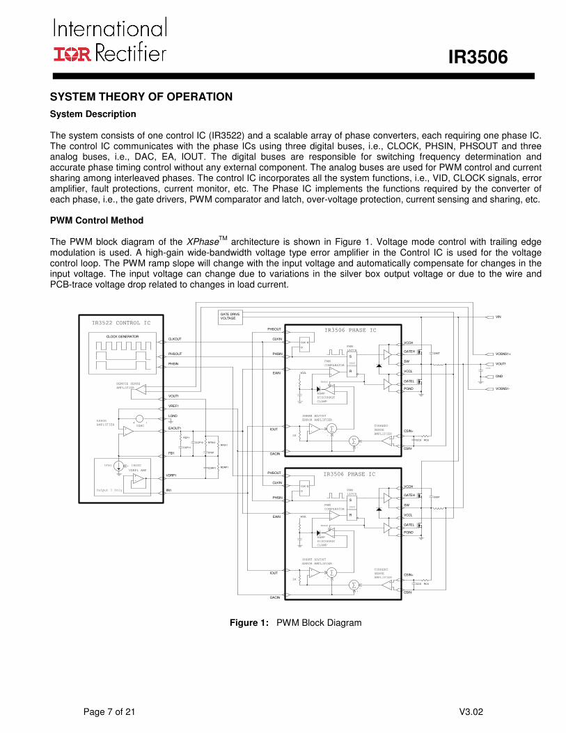
SYSTEM THEORY OF OPERATION
System Description The system consists of one control IC (IR3522) and a scalable array of phase converters, each requiring one phase IC. The control IC communicates with the phase ICs using three digital buses, i.e., CLOCK, PHSIN, PHSOUT and three analog buses, i.e., DAC, EA, IOUT. The digital buses are responsible for switching frequency determination and accurate phase timing control without any external component. The analog buses are used for PWM control and current sharing among interleaved phases. The control IC incorporates all the system functions, i.e., VID, CLOCK signals, error amplifier, fault protections, current monitor, etc. The Phase IC implements the functions required by the converter of each phase, i.e., the gate drivers, PWM comparator and latch, over-voltage protection, current sensing and sharing, etc. PWM Control Method The PWM block diagram of the XPhase
TM architecture is shown in Figure 1. Voltage mode control with trailing edge
modulation is used. A high-gain wide-bandwidth voltage type error amplifier in the Control IC is used for the voltage control loop. The PWM ramp slope will change with the input voltage and automatically compensate for changes in the input voltage. The input voltage can change due to variations in the silver box output voltage or due to the wire and PCB-trace voltage drop related to changes in load current.
GND
VOUT1
VOSNS1+
DACIN
VREF1
VOUT1
IIN1
VDRP1
LGND
IOUT
PHSIN
VOSNS1-
CSIN-
CSIN+
GATEL
EAIN
GATEH
SW
VIN
FB1
EAOUT1
CLKOUT CLKIN
PHSOUT
PGND
VCCL
VCCH
DACIN
CLKIN
PHSOUT
CSIN+
GATEL
EAIN
GATEH
IOUT
PHSIN
SW
PGND
VCCL
VCCH
CSIN-
PHSIN
PHSOUT
VID6VID6
IROSC
VID6
VID6
VID6VID6
VID6
VID6
VID6
VID6
GATE DRIVE
VOLTAGE
-
+
+
+
ENABLE
RAMP
DISCHARGE
CLAMP
IFB1
VDRP1 AMP
VDAC
CLOCK GENERATOR
CURRENT
SENSE
AMPLIFIER
R
S
SHARE ADJUST
ERROR AMPLIFIER
RESET
DOMINANT
PWM
LATCH
ERROR
AMPLIFIER
COUT
IR3522 CONTROL IC
IR3506 PHASE IC
Output 1 Only
PWM
COMPARATOR
PWM
COMPARATOR
VCCL
-
+
+
+
RAMP
DISCHARGE
CLAMP
ENABLE
SHARE ADJUST
ERROR AMPLIFIER
RESET
DOMINANT
PWM
LATCH
CURRENT
SENSE
AMPLIFIER
R
S
IR3506 PHASE IC
REMOTE SENSE
AMPLIFIER
VCCL
CCS RCS
+ -
CFB1
RCS
CBST
+
-
CCS
CBST
+
-
+
-
CCP11
+
-
+
-
RFB12
RDRP1CDRP1
RFB11
3K
CLK
D
Q
+
-
+
-
RCP1
+
-
3K
+
-
+
-
CCP12
CLK
D
Q
+
-
Figure 1: PWM Block Diagram
IR3506
Page 8 of 21 V3.02
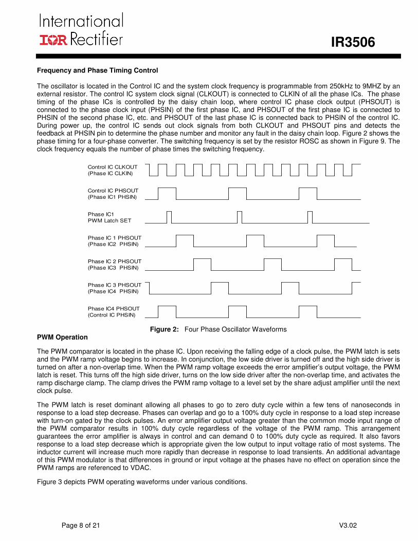
Frequency and Phase Timing Control The oscillator is located in the Control IC and the system clock frequency is programmable from 250kHz to 9MHZ by an external resistor. The control IC system clock signal (CLKOUT) is connected to CLKIN of all the phase ICs. The phase timing of the phase ICs is controlled by the daisy chain loop, where control IC phase clock output (PHSOUT) is connected to the phase clock input (PHSIN) of the first phase IC, and PHSOUT of the first phase IC is connected to PHSIN of the second phase IC, etc. and PHSOUT of the last phase IC is connected back to PHSIN of the control IC. During power up, the control IC sends out clock signals from both CLKOUT and PHSOUT pins and detects the feedback at PHSIN pin to determine the phase number and monitor any fault in the daisy chain loop. Figure 2 shows the phase timing for a four-phase converter. The switching frequency is set by the resistor ROSC as shown in Figure 9. The clock frequency equals the number of phase times the switching frequency.
Phase IC1
PWM Latch SET
Control IC CLKOUT
(Phase IC CLKIN)
Control IC PHSOUT
(Phase IC1 PHSIN)
Phase IC 1 PHSOUT
(Phase IC2 PHSIN)
Phase IC 2 PHSOUT
(Phase IC3 PHSIN)
Phase IC 3 PHSOUT
(Phase IC4 PHSIN)
Phase IC4 PHSOUT
(Control IC PHSIN)
Figure 2: Four Phase Oscillator Waveforms PWM Operation
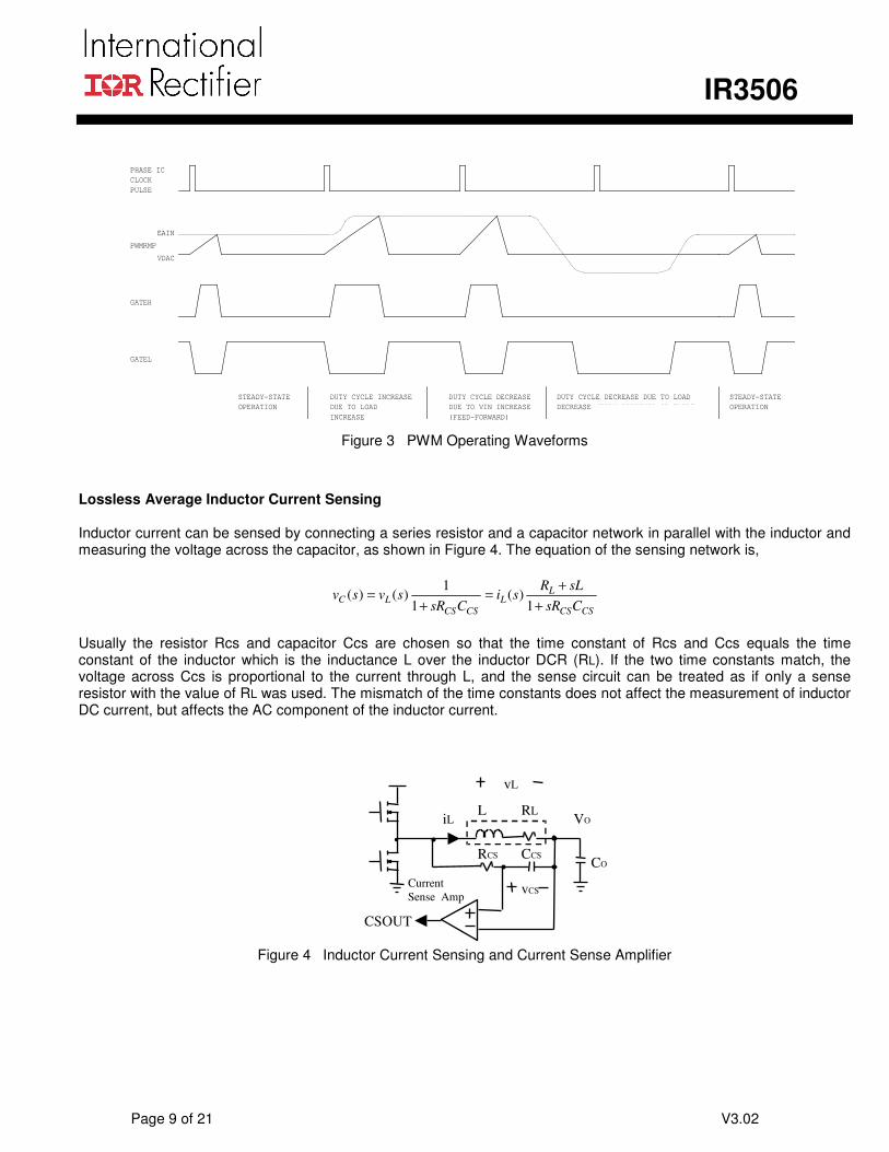
The PWM comparator is located in the phase IC. Upon receiving the falling edge of a clock pulse, the PWM latch is sets and the PWM ramp voltage begins to increase. In conjunction, the low side driver is turned off and the high side driver is turned on after a non-overlap time. When the PWM ramp voltage exceeds the error amplifier’s output voltage, the PWM latch is reset. This turns off the high side driver, turns on the low side driver after the non-overlap time, and activates the ramp discharge clamp. The clamp drives the PWM ramp voltage to a level set by the share adjust amplifier until the next clock pulse.
The PWM latch is reset dominant allowing all phases to go to zero duty cycle within a few tens of nanoseconds in response to a load step decrease. Phases can overlap and go to a 100% duty cycle in response to a load step increase with turn-on gated by the clock pulses. An error amplifier output voltage greater than the common mode input range of the PWM comparator results in 100% duty cycle regardless of the voltage of the PWM ramp. This arrangement guarantees the error amplifier is always in control and can demand 0 to 100% duty cycle as required. It also favors response to a load step decrease which is appropriate given the low output to input voltage ratio of most systems. The inductor current will increase much more rapidly than decrease in response to load transients. An additional advantage of this PWM modulator is that differences in ground or input voltage at the phases have no effect on operation since the PWM ramps are referenced to VDAC.
Figure 3 depicts PWM operating waveforms under various conditions.
IR3506
Page 9 of 21 V3.02
Figure 3 PWM Operating Waveforms
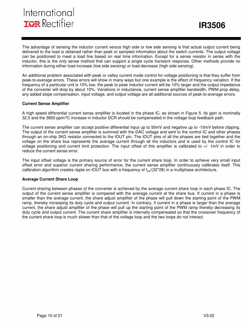
Lossless Average Inductor Current Sensing Inductor current can be sensed by connecting a series resistor and a capacitor network in parallel with the inductor and measuring the voltage across the capacitor, as shown in Figure 4. The equation of the sensing network is,
CSCS
L
L
CSCS
LCCsR
sLRsi
CsRsvsv
+
+=
+=
1)(
1
1)()(
Usually the resistor Rcs and capacitor Ccs are chosen so that the time constant of Rcs and Ccs equals the time constant of the inductor which is the inductance L over the inductor DCR (RL). If the two time constants match, the voltage across Ccs is proportional to the current through L, and the sense circuit can be treated as if only a sense resistor with the value of RL was used. The mismatch of the time constants does not affect the measurement of inductor DC current, but affects the AC component of the inductor current.
Figure 4 Inductor Current Sensing and Current Sense Amplifier
CO
L RL
RCS CCS
V O
Current
Sense Amp
CSOUT
iL
v L
vCS
PHASE IC
CLOCK
PULSE
EAIN
VDAC
PWMRMP
GATEH
GATEL
STEADY-STATE
OPERATION
DUTY CYCLE DECREASE
DUE TO VIN INCREASE
(FEED-FORWARD)
DUTY CYCLE INCREASE
DUE TO LOAD
INCREASE
STEADY-STATE
OPERATION
DUTY CYCLE DECREASE DUE TO LOAD
DECREASE (BODY BRAKING) OR FAULT
(VCCLUV, OCP, VID=11111X)
IR3506
Page 10 of 21 V3.02
The advantage of sensing the inductor current versus high side or low side sensing is that actual output current being delivered to the load is obtained rather than peak or sampled information about the switch currents. The output voltage can be positioned to meet a load line based on real time information. Except for a sense resistor in series with the inductor, this is the only sense method that can support a single cycle transient response. Other methods provide no information during either load increase (low side sensing) or load decrease (high side sensing). An additional problem associated with peak or valley current mode control for voltage positioning is that they suffer from peak-to-average errors. These errors will show in many ways but one example is the effect of frequency variation. If the frequency of a particular unit is 10% low, the peak to peak inductor current will be 10% larger and the output impedance of the converter will drop by about 10%. Variations in inductance, current sense amplifier bandwidth, PWM prop delay, any added slope compensation, input voltage, and output voltage are all additional sources of peak-to-average errors. Current Sense Amplifier
A high speed differential current sense amplifier is located in the phase IC, as shown in Figure 5. Its gain is nominally 32.5 and the 3850 ppm/ºC increase in inductor DCR should be compensated in the voltage loop feedback path.
The current sense amplifier can accept positive differential input up to 50mV and negative up to -10mV before clipping. The output of the current sense amplifier is summed with the DAC voltage and sent to the control IC and other phases through an on-chip 3KΩ resistor connected to the IOUT pin. The IOUT pins of all the phases are tied together and the voltage on the share bus represents the average current through all the inductors and is used by the control IC for voltage positioning and current limit protection. The input offset of this amplifier is calibrated to +/- 1mV in order to reduce the current sense error. The input offset voltage is the primary source of error for the current share loop. In order to achieve very small input offset error and superior current sharing performance, the current sense amplifier continuously calibrates itself. This calibration algorithm creates ripple on IOUT bus with a frequency of fsw/(32*28) in a multiphase architecture. Average Current Share Loop Current sharing between phases of the converter is achieved by the average current share loop in each phase IC. The output of the current sense amplifier is compared with the average current at the share bus. If current in a phase is smaller than the average current, the share adjust amplifier of the phase will pull down the starting point of the PWM ramp, thereby increasing its duty cycle and output current. In contrary, if current in a phase is larger than the average current, the share adjust amplifier of the phase will pull up the starting point of the PWM ramp thereby decreasing its duty cycle and output current. The current share amplifier is internally compensated so that the crossover frequency of the current share loop is much slower than that of the voltage loop and the two loops do not interact.
IR3506
Page 11 of 21 V3.02
IR3506 THEORY OF OPERATION
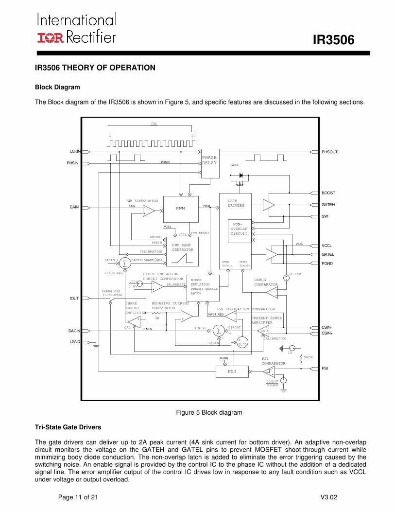
Block Diagram The Block diagram of the IR3506 is shown in Figure 5, and specific features are discussed in the following sections.
EAIN EAIN
PWM COMPARATOR
+
-
+
-
CSIN-
CSIN+
DEBUG
COMPARATOR
0.15V
PSI
500K
610mV510mV
+
-
1V
PSI
COMPARATOR
75PCT_REG
CSAOUT
CALIBRATION
DACIN
+
-
IROSC
IROSC
CURRENT SENSE
AMPLIFIER
X32.5+
75% REGULATION COMPARATOR
X
0.75
+
+
-
PHSINPHSIN
DIODE EMULATION
PRESET COMPARATOR
0.8V+
-
VCCLDE_PRESET
IOUT
DIODE
EMULATION
PRESET ENABLE
LATCH
PHASE
DELAY
NON-
OVERLAP
CIRCUIT
CAL
SHARE
ADJUST
AMPLIFIER
+
-
NEGATIVE CURRENT
COMPARATOR
3K+
-
LGND
DACINDACIN
VCCL
PSI
BOOST
GATEH
SW
GATE
DRIVERS
VCCL
DACIN
SHARE_ADJ
-
+PGND
GATEL
VCCL
PHSOUT
VCCL
GATEL
Disable
DEBUG OFF
(LOW=OPEN)
PWM
15
CAL
CLKIN
1
PWM
RMPOUT
CALIBRATION
PWM RESET
PHSIN
VCCL
DACIN-SHARE_ADJ
PWM RAMP
GENERATOR
GATEs
Disable
PHSIN
Figure 5 Block diagram Tri-State Gate Drivers The gate drivers can deliver up to 2A peak current (4A sink current for bottom driver). An adaptive non-overlap circuit monitors the voltage on the GATEH and GATEL pins to prevent MOSFET shoot-through current while minimizing body diode conduction. The non-overlap latch is added to eliminate the error triggering caused by the switching noise. An enable signal is provided by the control IC to the phase IC without the addition of a dedicated signal line. The error amplifier output of the control IC drives low in response to any fault condition such as VCCL under voltage or output overload.
IR3506
Page 12 of 21 V3.02
A synchronous rectification disable comparator is used to detect converter CSIN- pin voltage, which represents local converter output voltage. If the voltage is below 75% of VOUT1 and negative current is detected during startup, GATEL drives low, which disables synchronous rectification and eliminates negative current during power-up. Once VOUT1 reaches approximately 75 % of its nominal value, synchronous rectification is regain and can not be disable again until the startup. The gate drivers pull low if the supply voltages are below the normal operating range. An 80kΩ resistor is connected across the GATEH/GATEL and PGND pins to prevent the GATEH/GATEL voltage from rising due to leakage or other causes under these conditions.
Over Voltage Protection (OVP) Output over-voltage might occur due to a high side MOSFET short or if the output voltage sense path is compromised. If the over-voltage protection comparators sense that either VOUT1 pin voltage exceeds VREF1 by 260mV or VOUT2 exceeds VREF1, the over voltage fault latch is set which pulls the error amplifier output low to turn off the converter power stage. The IR3522 communicates an OVP condition to the system by raising the CROWBAR pin voltage to within V(VCCL) – 0.2 V. With the error amplifiers outputs low, the low-side MOSFET turn-on within approximately 150ns. The low side MOSFET will remain low until the over voltage fault condition latch cleared.
IR3506
Page 13 of 21 V3.02
PWM Ramp
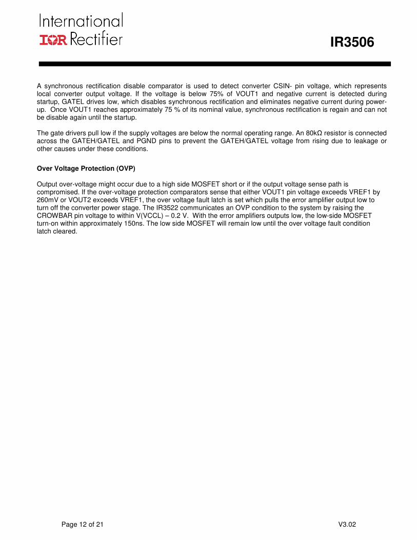
Every time the phase IC is powered up, PWM ramp magnitude is calibrated to generate a 53 mV/%DC. For example, for a 15 % duty ratio the ramp amplitude is 795mV. In response to a load step-up, the error amplifier can demand 100 % duty cycle. In order to avoid pulse skipping under this scenario and allow the BOOST cap to replenish, a minimum off-time is allowed in this mode of operation. As shown in Figure 6, 100 % duty is detected by comparing the PWM latch output (PWMQ) and its input clock (PWM_CLK). If the PWMQ is high when the PWM_CLK is asserted, the TopFET turnoff is initiated. The TopFET is again turned on once the RMPOUT drops within 200 mV of the VDAC.
PHOUT
CLKIN
EAIN
(2 Phase Design)
RMPOUT
PWMQ
100 % DUTY OPERATIONNORMAL OPERATION
Figure 1: PWM Operation during normal and 100 % duty mode.
Power State Indicator (PSI) function From a system perspective, the PSI input is controlled by the system and is forced low when the load current is lower than a preset limit and forced high when load current is higher than the preset limit. IR3506 can accept an active low signal on its PSI input and force the drivers into tri-state, effectively forcing the phase IC into off state. A PSI-assert signal activates three features in the Phase IC. 1) It disconnects the IOUT pin from the IOUT bus: From a system perspective, IOUT is used to report current and is used for over-current protection. By disconnecting the disabled phase from the IOUT bus, proper current reporting and over-current protection level is ensured. 2) The DFF is disabled and it appears as a pass-through to the daisy chain loop: By removing the DFF from the daisy chain, the system ensures that proper phase delay is activated among the active phases. 3) The gate drivers are forced to tri-state, effectively, disabling the phase IC: Figure 7 shows the impact of PSI-assert on the gate drivers. After 8 cycle PHSIN delay, at the next CLK falling edge, the PSI_SYNC goes from 0 to 1. This disables the gate drives and shorts the DFF.

IR3506
Page 14 of 21 V3.02
PSI_SYNC
PSI 8 PHSIN Delay
D_PWM LATCH
CLK
Figure 2: PSI assertion. Debugging Mode
If CSIN+ pin is pulled up to VCCL voltage, IR3506 enters into debugging mode. Both drivers are pulled low and IOUT output is disconnected from the current share bus, which isolates this phase IC from other phases. However, the phase timing from PHSIN to PHSOUT does not change. Emulated Bootstrap Diode IR3506 integrates a PFET to emulate the bootstrap diode. If two or more top MOSFETs are to be driven at higher switching frequency, an external bootstrap diode connected from VCCL pin to BOOST pin may be needed.
Operation at Higher Output Voltage
The proper operation of the phase IC is ensured for maximum output voltage up to VCCL-2.5V if the differential input (CSIN(+) – CSIN(-)) to current sense amplifier remain below 30 mV. Otherwise, the maximum voltage output is calculated with the following equation:
),(*5.1max_−+
−−−=CSINCSIN
VVGcsVCCLVo
where, Gcs is the current sense amplifier gain (typically 32.5).

IR3506
Page 15 of 21 V3.02
DESIGN PROCEDURES - IR3506
Inductor Current Sensing Capacitor CCS and Resistor RCS
The DC resistance of the inductor is utilized to sense the inductor current. Usually the resistor RCS and capacitor CCS in parallel with the inductor are chosen to match the time constant of the inductor, and therefore the voltage across the capacitor CCS represents the inductor current. If the two time constants are not the same, the AC component of the capacitor voltage is different from that of the real inductor current. The time constant mismatch does not affect the average current sharing among the multiple phases, but does effect the current signal IOUT as well as the output voltage during the load current transient if adaptive voltage positioning is adopted. Measure the inductance L and the inductor DC resistance RL. Pre-select the capacitor CCS and calculate RCS as follows.
CS
L
CSC
RLR = (1)
Bootstrap Capacitor CBST
Depending on the duty cycle and gate drive current of the phase IC, a capacitor in the range of 0.1uF to 1uF is needed for the bootstrap circuit.
Decoupling Capacitors for Phase IC
A 0.1uF-1uF decoupling capacitor is required at the VCCL pin.
CURRENT SHARE LOOP COMPENSATION
The internal compensation of current share loop ensures that crossover frequency of the current share loop is at least one decade lower than that of the voltage loop so that the interaction between the two loops is eliminated. The crossover frequency of current share loop is approximately 8 kHz.
IR3506
Page 16 of 21 V3.02
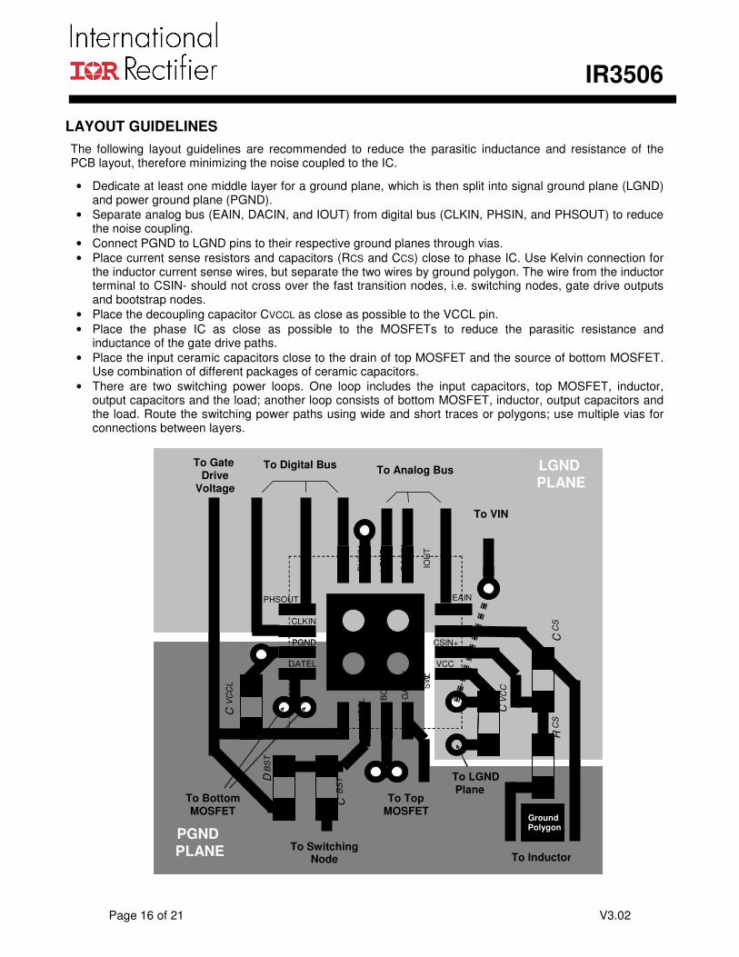
LAYOUT GUIDELINES
The following layout guidelines are recommended to reduce the parasitic inductance and resistance of the PCB layout, therefore minimizing the noise coupled to the IC.
• Dedicate at least one middle layer for a ground plane, which is then split into signal ground plane (LGND) and power ground plane (PGND).
• Separate analog bus (EAIN, DACIN, and IOUT) from digital bus (CLKIN, PHSIN, and PHSOUT) to reduce the noise coupling.
• Connect PGND to LGND pins to their respective ground planes through vias.
• Place current sense resistors and capacitors (RCS and CCS) close to phase IC. Use Kelvin connection for the inductor current sense wires, but separate the two wires by ground polygon. The wire from the inductor terminal to CSIN- should not cross over the fast transition nodes, i.e. switching nodes, gate drive outputs and bootstrap nodes.
• Place the decoupling capacitor CVCCL as close as possible to the VCCL pin.
• Place the phase IC as close as possible to the MOSFETs to reduce the parasitic resistance and inductance of the gate drive paths.
• Place the input ceramic capacitors close to the drain of top MOSFET and the source of bottom MOSFET. Use combination of different packages of ceramic capacitors.
• There are two switching power loops. One loop includes the input capacitors, top MOSFET, inductor, output capacitors and the load; another loop consists of bottom MOSFET, inductor, output capacitors and the load. Route the switching power paths using wide and short traces or polygons; use multiple vias for connections between layers.
PGND
GATEL VCCL GATEHBOOST
VCC
EAIN
To Digital Bus
To Inductor
To LGND Plane
C
VCCL
To VIN
D
BST
SW
C
BST
To Gate Drive
Voltage
PHSIN LGND DACIN ISHARE
CSIN -
PHSOUT
CLKIN
To TopMOSFET
PGND
PLANE
LGNDPLANE
Ground Polygon
C
VCC
R
CS
C
CS
To BottomMOSFET
To Analog Bus
To SwitchingNode
R
PGND
GATEL
VC
CL G
AT
EH
BO
OS
T VCC
EAIN
To Digital Bus
To Inductor
To LGND Plane
C V
CC
L
To VIN
D B
ST
SW
C B
ST
To Gate Drive
Voltage
PH
SIN
LG
ND
DA
CIN
IOU
T
PHSOUT
CLKIN
To TopMOSFET
PGND
PLANE
LGNDPLANE
Ground Polygon
C V
CC
R C
S
C C
S
To BottomMOSFET
To Analog Bus
To SwitchingNode
CSIN+
IR3506
Page 17 of 21 V3.02
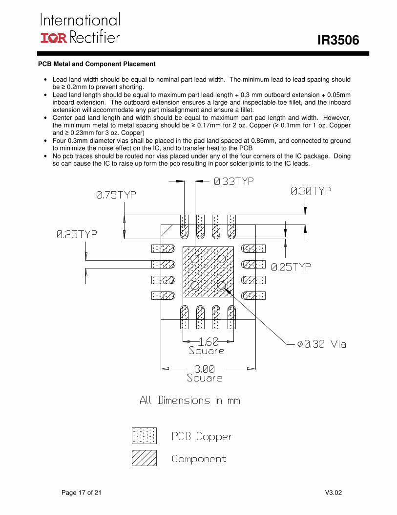
PCB Metal and Component Placement
• Lead land width should be equal to nominal part lead width. The minimum lead to lead spacing should be ≥ 0.2mm to prevent shorting.
• Lead land length should be equal to maximum part lead length + 0.3 mm outboard extension + 0.05mm inboard extension. The outboard extension ensures a large and inspectable toe fillet, and the inboard extension will accommodate any part misalignment and ensure a fillet.
• Center pad land length and width should be equal to maximum part pad length and width. However, the minimum metal to metal spacing should be ≥ 0.17mm for 2 oz. Copper (≥ 0.1mm for 1 oz. Copper and ≥ 0.23mm for 3 oz. Copper)
• Four 0.3mm diameter vias shall be placed in the pad land spaced at 0.85mm, and connected to ground to minimize the noise effect on the IC, and to transfer heat to the PCB
• No pcb traces should be routed nor vias placed under any of the four corners of the IC package. Doing so can cause the IC to raise up form the pcb resulting in poor solder joints to the IC leads.
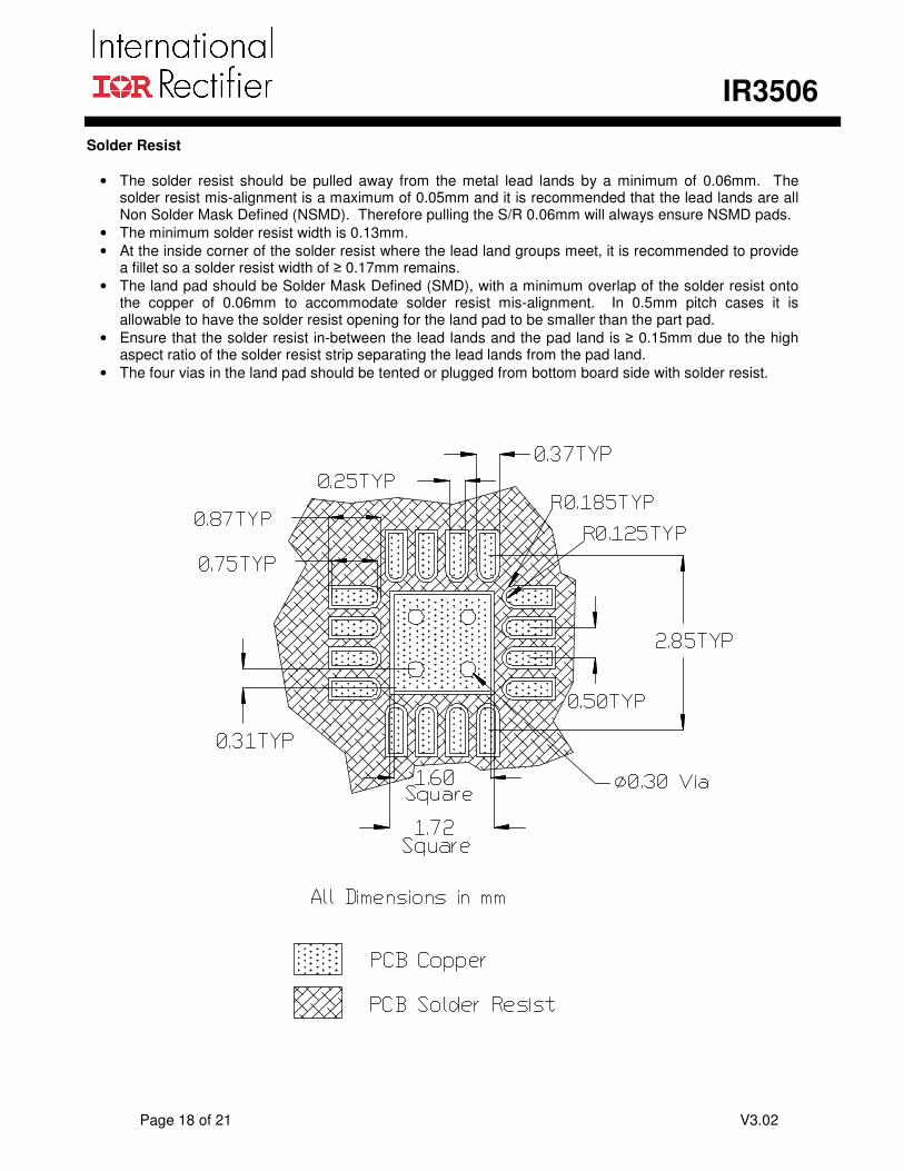
IR3506
Page 18 of 21 V3.02
Solder Resist
• The solder resist should be pulled away from the metal lead lands by a minimum of 0.06mm. The solder resist mis-alignment is a maximum of 0.05mm and it is recommended that the lead lands are all Non Solder Mask Defined (NSMD). Therefore pulling the S/R 0.06mm will always ensure NSMD pads.
• The minimum solder resist width is 0.13mm.
• At the inside corner of the solder resist where the lead land groups meet, it is recommended to provide a fillet so a solder resist width of ≥ 0.17mm remains.
• The land pad should be Solder Mask Defined (SMD), with a minimum overlap of the solder resist onto the copper of 0.06mm to accommodate solder resist mis-alignment. In 0.5mm pitch cases it is allowable to have the solder resist opening for the land pad to be smaller than the part pad.
• Ensure that the solder resist in-between the lead lands and the pad land is ≥ 0.15mm due to the high aspect ratio of the solder resist strip separating the lead lands from the pad land.
• The four vias in the land pad should be tented or plugged from bottom board side with solder resist.
IR3506
Page 19 of 21 V3.02
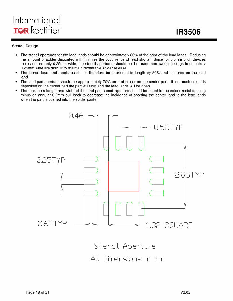
Stencil Design
• The stencil apertures for the lead lands should be approximately 80% of the area of the lead lands. Reducing the amount of solder deposited will minimize the occurrence of lead shorts. Since for 0.5mm pitch devices the leads are only 0.25mm wide, the stencil apertures should not be made narrower; openings in stencils < 0.25mm wide are difficult to maintain repeatable solder release.
• The stencil lead land apertures should therefore be shortened in length by 80% and centered on the lead land.
• The land pad aperture should be approximately 70% area of solder on the center pad. If too much solder is deposited on the center pad the part will float and the lead lands will be open.
• The maximum length and width of the land pad stencil aperture should be equal to the solder resist opening minus an annular 0.2mm pull back to decrease the incidence of shorting the center land to the lead lands when the part is pushed into the solder paste.
IR3506
Page 20 of 21 V3.02
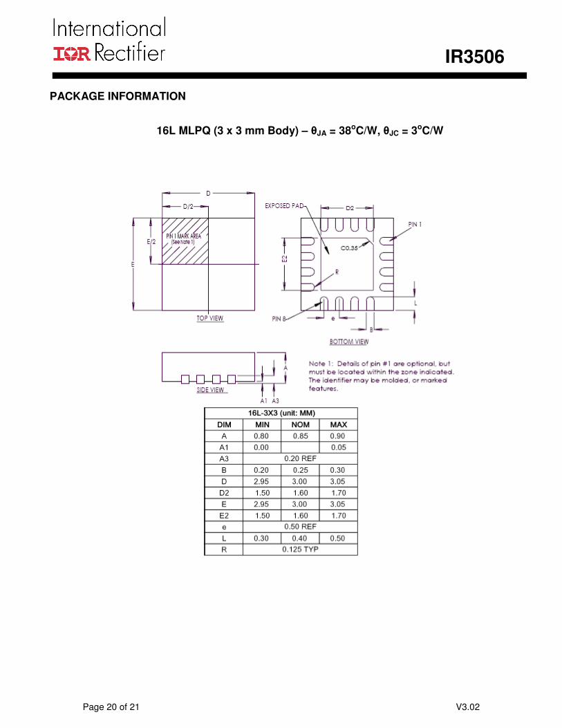
PACKAGE INFORMATION
16L MLPQ (3 x 3 mm Body) – θJA = 38oC/W, θJC = 3oC/W
IR3506
Page 21 of 21 V3.02
Data and specifications subject to change without notice. This product has been designed and qualified for the Consumer market.
Qualification Standards can be found on IR’s Web site.
IR WORLD HEADQUARTERS: 233 Kansas St., El Segundo, California 90245, USA Tel: (310) 252-7105 TAC Fax: (310) 252-7903
Visit us at www.irf.com for sales contact information. www.irf.com

Mouser Electronics
Authorized Distributor
Click to View Pricing, Inventory, Delivery & Lifecycle Information: International Rectifier:
IR3506MTRPBF