Embed Size (px)
Citation preview

IPSEC IMPLEMENTATION IN EMBEDDED SYSTEMS FORPARTIAL RECONFIGURABLE PLATFORMS
by
Ahmad SalmanA Thesis
Submitted to theGraduate Faculty
ofGeorge Mason UniversityIn Partial fulfillment of
The Requirements for the Degreeof
Master of ScienceComputer Engineering
Committee:
Dr. Jens-Peter Kaps, Thesis Director
Dr. Kris Gaj, Committee Member
Dr. Craig Lorie, Committee Member
Dr. Andre Manitius, Chairman, Departmentof Electrical and Computer Engineering
Dr. Lloyd J. Griffiths, Dean, VolgenauSchool of Engineering
Date: Summer Semester 2011George Mason UniversityFairfax, VA

IPsec Implementation in Embedded Systems forPartial Reconfigurable Platforms
A thesis submitted in partial fulfillment of the requirements for the degree ofMaster of Science at George Mason University
By
Ahmad SalmanBachelor of Engineering
Arab Academy for Science and Technology, 2002
Director: Dr. Jens-Peter Kaps, ProfessorDepartment of Electrical and Computer Engineering
Summer Semester 2011George Mason University
Fairfax, VA

Copyright c© 2011 by Ahmad SalmanAll Rights Reserved
ii

Dedication
I dedicate this thesis to my parents, Ali Salman and Fatma Mahmoud, my sisters Mona,Hadeel and Inas, my brother Akram for believing in me and for their endless support.
iii

Acknowledgments
First I wish to thank my advisor Dr. Jens-Peter Kaps for his guidance, support and end-less patience during the time it took me to finish the thesis work and for making all theresources and equipment I needed available. I’m really fortunate to have him as an advisorand teacher.
Secondly, I would like to thank Dr. Kris Gaj for his valuable input, guidance and remarksand and Dr. David Hwang for pointing me to the right direction and providing a startingpoint for the thesis as well as valuable resources. I’d also like to thank Dr. Craig Lorie forthe time he provided, valuable comments and for understanding when I did not fulfill myduties as his TA on time during my thesis work.
Finally, a special thanks to my friend and colleague Marcin Rogawski for his help, sup-port and providing valuable resources essential to finishing this thesis. I’d like to thank allmy friends and colleagues in the Cryptographic Engineering Research Group (CERG) fortheir help and support.
iv

Table of Contents
Page
List of Tables . . . . . . . . . . . . . . . . . . . . . . . . . . . . . . . . . . . . . . . . vii
List of Figures . . . . . . . . . . . . . . . . . . . . . . . . . . . . . . . . . . . . . . . . viii
Abstract . . . . . . . . . . . . . . . . . . . . . . . . . . . . . . . . . . . . . . . . . . . ix
1 Introduction . . . . . . . . . . . . . . . . . . . . . . . . . . . . . . . . . . . . . . 1
1.1 Overview . . . . . . . . . . . . . . . . . . . . . . . . . . . . . . . . . . . . . 1
1.2 Method . . . . . . . . . . . . . . . . . . . . . . . . . . . . . . . . . . . . . . 2
1.3 Thesis Outline . . . . . . . . . . . . . . . . . . . . . . . . . . . . . . . . . . 3
2 Related Work and Motivation . . . . . . . . . . . . . . . . . . . . . . . . . . . . 4
2.1 Hardware Implementations and FPGA . . . . . . . . . . . . . . . . . . . . . 4
2.2 IPsec . . . . . . . . . . . . . . . . . . . . . . . . . . . . . . . . . . . . . . . . 5
2.3 IP Cores . . . . . . . . . . . . . . . . . . . . . . . . . . . . . . . . . . . . . . 8
3 Background . . . . . . . . . . . . . . . . . . . . . . . . . . . . . . . . . . . . . . . 9
3.1 Overview . . . . . . . . . . . . . . . . . . . . . . . . . . . . . . . . . . . . . 9
3.2 Boards . . . . . . . . . . . . . . . . . . . . . . . . . . . . . . . . . . . . . . . 9
3.2.1 XUP Virtex-II-Pro Development System . . . . . . . . . . . . . . . . 9
3.2.2 ML403 Evaluation Platform . . . . . . . . . . . . . . . . . . . . . . . 11
3.3 FPGA Architecture . . . . . . . . . . . . . . . . . . . . . . . . . . . . . . . 13
3.3.1 XC2VP30 FPGA . . . . . . . . . . . . . . . . . . . . . . . . . . . . . 13
3.3.2 XC4VFX12 FPGA . . . . . . . . . . . . . . . . . . . . . . . . . . . . 14
3.4 Configuration . . . . . . . . . . . . . . . . . . . . . . . . . . . . . . . . . . . 15
3.4.1 XUP Virtex-II-Pro Configuration . . . . . . . . . . . . . . . . . . . . 15
3.4.2 ML403 Configuration . . . . . . . . . . . . . . . . . . . . . . . . . . 16
3.5 Tools . . . . . . . . . . . . . . . . . . . . . . . . . . . . . . . . . . . . . . . . 16
3.5.1 Xilinx Embedded Development Kit (EDK) . . . . . . . . . . . . . . 16
3.5.2 Xilinx Integrated Software Environment (ISE) . . . . . . . . . . . . 17
3.5.3 PlanAhead . . . . . . . . . . . . . . . . . . . . . . . . . . . . . . . . 18
3.6 Partial Reconfiguration . . . . . . . . . . . . . . . . . . . . . . . . . . . . . 19
3.6.1 Introduction . . . . . . . . . . . . . . . . . . . . . . . . . . . . . . . 19
3.6.2 Early Access Partial Reconfiguration . . . . . . . . . . . . . . . . . . 20
v

3.6.3 Internal Configuration Access Port . . . . . . . . . . . . . . . . . . . 22
3.6.4 Bus Macros . . . . . . . . . . . . . . . . . . . . . . . . . . . . . . . . 24
4 Implementation Methodology . . . . . . . . . . . . . . . . . . . . . . . . . . . . . 27
4.1 Overview . . . . . . . . . . . . . . . . . . . . . . . . . . . . . . . . . . . . . 27
4.2 Design Description Overview . . . . . . . . . . . . . . . . . . . . . . . . . . 28
4.3 Hardware Architecture . . . . . . . . . . . . . . . . . . . . . . . . . . . . . . 30
4.3.1 Processor Cores and Buses . . . . . . . . . . . . . . . . . . . . . . . 30
4.3.2 Software Architecture . . . . . . . . . . . . . . . . . . . . . . . . . . 40
4.3.3 Hardware-Software Synchronization . . . . . . . . . . . . . . . . . . 43
5 Experiment Methodology . . . . . . . . . . . . . . . . . . . . . . . . . . . . . . . 48
5.1 Overview . . . . . . . . . . . . . . . . . . . . . . . . . . . . . . . . . . . . . 48
5.2 Static Portion Of The System . . . . . . . . . . . . . . . . . . . . . . . . . . 48
5.3 Dynamic Portion Of The System . . . . . . . . . . . . . . . . . . . . . . . . 49
5.4 Design Synthesis and Top-Level creation . . . . . . . . . . . . . . . . . . . . 50
5.5 Design Floorplanning and Implementation . . . . . . . . . . . . . . . . . . . 50
5.6 Problems . . . . . . . . . . . . . . . . . . . . . . . . . . . . . . . . . . . . . 53
6 Results . . . . . . . . . . . . . . . . . . . . . . . . . . . . . . . . . . . . . . . . . 55
6.1 Device Utilization Summary . . . . . . . . . . . . . . . . . . . . . . . . . . . 55
6.2 Time Measurements . . . . . . . . . . . . . . . . . . . . . . . . . . . . . . . 58
7 Conclusion . . . . . . . . . . . . . . . . . . . . . . . . . . . . . . . . . . . . . . . 61
vi

List of Tables
Table Page
2.1 IPsec Supported Protocols and Algorithms . . . . . . . . . . . . . . . . . . 7
3.1 XC4VFX12 Basic Features . . . . . . . . . . . . . . . . . . . . . . . . . . . 14
6.1 Resources Summary for Implementations on ML403 Board . . . . . . . . . . 55
6.2 Resources Summary for PowerPC Implementations on Virtex-II-Pro . . . . 57
6.3 Resources Summary for Microblaze Implementations on Virtex-II-Pro . . . 58
6.4 Average Reconfiguration Speed on Both Platforms For Two Different Designs 60
vii

List of Figures
Figure Page
1.1 A High-Level Diagram of the Design . . . . . . . . . . . . . . . . . . . . . . 3
2.1 Authentication Header and Encapsulating Security Payload Formats . . . . 6
3.1 XUP Virtex II-Pro Board and Some Peripherals . . . . . . . . . . . . . . . 10
3.2 ML403 Board and Some Peripherals . . . . . . . . . . . . . . . . . . . . . . 12
3.3 ICAP Configuration Process . . . . . . . . . . . . . . . . . . . . . . . . . . . 23
3.4 Bus Macros Used to Lock Routing Between PRMs and BDM . . . . . . . . 24
4.1 Embedded System Processor and Peripherals . . . . . . . . . . . . . . . . . 29
4.2 AES Datapath . . . . . . . . . . . . . . . . . . . . . . . . . . . . . . . . . . 34
4.3 Top-Level Diagram for AES Encryption Module . . . . . . . . . . . . . . . 35
4.4 Top-Level Diagram for AES Wrapper . . . . . . . . . . . . . . . . . . . . . . 35
4.5 AES Wrapper . . . . . . . . . . . . . . . . . . . . . . . . . . . . . . . . . . . 36
4.6 SHA-256 Datapath . . . . . . . . . . . . . . . . . . . . . . . . . . . . . . . . 37
4.7 SHA-256 Datapath . . . . . . . . . . . . . . . . . . . . . . . . . . . . . . . . 38
4.8 SHA-256 Wrapper . . . . . . . . . . . . . . . . . . . . . . . . . . . . . . . . 38
4.9 SHA-256 Command Flag . . . . . . . . . . . . . . . . . . . . . . . . . . . . 39
4.10 Synchronization Circuit Between Hardware and Software . . . . . . . . . . . 45
4.11 Logic Analyzer Waveform Triggered at src ready . . . . . . . . . . . . . . . 46
4.12 Logic Analyzer Waveform Triggered at dst ready . . . . . . . . . . . . . . . 47
5.1 Virtex-II-PRO FPGA After Floorplanning . . . . . . . . . . . . . . . . . . . 51
5.2 Virtex-4 FPGA After Floorplanning . . . . . . . . . . . . . . . . . . . . . . 51
5.3 Virtex-II-PRO FPGA After Implementation . . . . . . . . . . . . . . . . . . 52
5.4 Virtex-4 FPGA After Implementation . . . . . . . . . . . . . . . . . . . . . 53
6.1 Total Time Needed for Partial Reconfiguration . . . . . . . . . . . . . . . . 59
viii
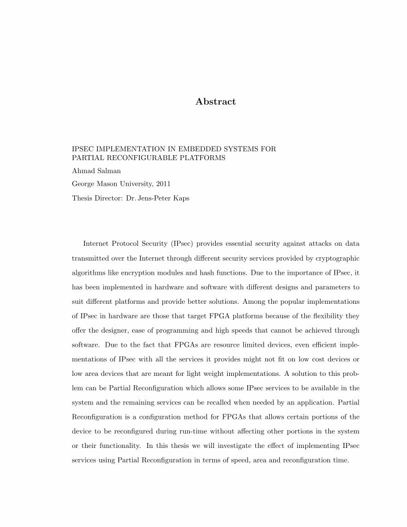
Abstract
IPSEC IMPLEMENTATION IN EMBEDDED SYSTEMS FORPARTIAL RECONFIGURABLE PLATFORMS
Ahmad Salman
George Mason University, 2011
Thesis Director: Dr. Jens-Peter Kaps
Internet Protocol Security (IPsec) provides essential security against attacks on data
transmitted over the Internet through different security services provided by cryptographic
algorithms like encryption modules and hash functions. Due to the importance of IPsec, it
has been implemented in hardware and software with different designs and parameters to
suit different platforms and provide better solutions. Among the popular implementations
of IPsec in hardware are those that target FPGA platforms because of the flexibility they
offer the designer, ease of programming and high speeds that cannot be achieved through
software. Due to the fact that FPGAs are resource limited devices, even efficient imple-
mentations of IPsec with all the services it provides might not fit on low cost devices or
low area devices that are meant for light weight implementations. A solution to this prob-
lem can be Partial Reconfiguration which allows some IPsec services to be available in the
system and the remaining services can be recalled when needed by an application. Partial
Reconfiguration is a configuration method for FPGAs that allows certain portions of the
device to be reconfigured during run-time without affecting other portions in the system
or their functionality. In this thesis we will investigate the effect of implementing IPsec
services using Partial Reconfiguration in terms of speed, area and reconfiguration time.

For that, we built an embedded system controlled through an embedded processor to
provide self reconfiguration of the system through a software application. We also imple-
mented different versions of the embedded system using Microblaze and PowerPC embedded
processors targeting two different platforms (Virtex-4 and Virtex-II-Pro) to perform thor-
ough testing on the proposed design and analyze the results.

Chapter 1: Introduction
1.1 Overview
In the last decade, the number of Internet users has increased by more than one billion
users with a growth rate of 444.8% making the Internet users count to be a little over one
fourth of the world population [1]. The use of the Internet by this huge number of users
and groups vary from social interacting and networking to economical and on-line banking.
This rapid increase in the number of users has opened the door to an increasing number of
security threats and cyber attacks making the need for a secure system for Internet usage
and global networks in general an essential demand. Internet Protocol Security (IPsec)
is a security protocol that provides security against a number of cyber attacks including
Eavesdropping, Hacking, Phishing and IP Spoofing [2] through a number of security services
like confidentiality, data integrity and authentication. Due to the overwhelming amount of
data transfered over global networks, software implementations of protocols like IPsec have
become impractical as software implementations cannot handle this much data processing
and computations within a reasonable response time [3].For this reason, such computations
are performed in hardware.
Hardware implementations not only perform at significantly higher speeds compared to
software, but they also provide better protection to schemes implemented on them against
attacks that software implementations are vulnerable to like viruses. Field Programmable
Gate Arrays (FPGA) have become more popular as platforms for hardware implementa-
tions due to the fact that they provide flexibility, fast production time-line and are cost
effective. For these reasons, they have been used as hardware accelerators in routers and
other network devices to implement protocols like IPsec and Secure Socket Layer (SSL)
1

[4]. One of the major advantages FPGA platforms provide is reconfigurability which facili-
tates system updates and upgrades. A relatively new feature of FPGA platforms, is Partial
Reconfiguration in which part of the chip is reconfigured while the remaining portion is
operational giving designers more options to efficiently use available resources.
Design implementations that take advantage of partial reconfiguration have shown promis-
ing results in terms of area saving and reduction in power consumption [5]. Although there
are a number of researches on IPsec implementations on FPGA platforms, non of them
take advantage of partial reconfiguration for efficient resource usage which can be benefi-
cial to light-weight implementations targeting resource limited platforms. We would like to
introduce a System-on-Chip (SoC) embedded system capable of performing IPsec protocol
services in hardware having only the modules that are in use at any given time residing on
the chip using partial reconfiguration.We will examine how useful such systems can be in
terms of saving area and the amount of time needed to partially reconfigure the system. In
the next sections we will present the method we used to achieve our goal and the outline of
the thesis.
1.2 Method
The embedded system we are proposing is composed of an embedded microprocessor, hard-
ware modules to perform IPsec operations in hardware, system supporting peripherals and
software support to create an Application Programming Interface (API) for different on-chip
peripherals. Figure 1.1 shows a high level diagram with major components of the design.
The embedded processor used in the system is either a Microblaze or PowerPC which will
be discussed later. This embedded processor controls partial reconfiguration of the system
through a module called the Internal Control Access Port (ICAP) which allows the system
to be self-reconfigurable without user involvement.
Partial reconfiguration of the system takes place between two Intellectual Property (IP)
Cores one is to perform encryption operations required by IPsec to provide confidentiality
2

Memory
Embedded
ProcessorIPsec
Coprocessor
Software ICAP
External
Figure 1.1: A High-Level Diagram of the Design.
and the other core is to perform hash calculations to provide authentication and data in-
tegrity. Depending on the application being processed by IPsec and the services required,
the microprocessor performs partial reconfiguration to load the suitable core for the re-
quested operation.
Xilinx ISE,EDK and PlanAhead tools were used through out different design and im-
plementation phases of the embedded system.The target devices for the created designs are
Virtex-II-Pro and Virtex-4 devices on XUP Virtex-II-Pro and ML403 boards, respectively.
1.3 Thesis Outline
The thesis will be organized as follows. Chapter 2 presents the related work and motivation.
In chapter 3 an overview of the target platforms, the FPGA devices on them, Xilinx tools
used and partial reconfiguration technique will be presented. Chapter 4 explains the hard-
ware architecture with different modules in the system as well as the software. In chapter 5
we present the implementation methodology and different design phases. In Chapter 6 the
results are presented and discussed. Finally, chapter 7 provides the thesis conclusion.
3

Chapter 2: Related Work and Motivation
2.1 Hardware Implementations and FPGA
In the past few years, hardware implementations of some network protocols, especially those
related to providing network security services like IPsec and Secure Socket Layer (SSL), have
increased due to the fact that data transfer rates have increased to the level of Tera-bits
per second which demands shorter response time and higher processing speed for data
which cannot be achieved through traditional software implementations that fails to handle
high data throughput rates. One of the known platforms for hardware implementations
of network security protocols is Network Security Processors (NSP) which can perform
various cryptographic operations specified by these network security protocols [6]. But like
Application Specific Integrated Circuit (ASIC) solutions, NSPs do not offer much flexibility
as they are not re-programmable platforms[7]. Field Programmable Gate Arrays (FPGA)
offer a System-on-Chip (SoC) solution with more flexibility for hardware implementations.
The main advantages that FPGA implementations have over ASICs are
• With FPGAs, it is possible to reconfigure the chip for different encryption standards
and hash algorithms to provide the services offered by different security services.
• Bug fixes in an existing implementation or upgrades to new standard can be easily
achieved with little to no cost.
• FPGAs offer lower cost for small volumes, shorter development times and faster time
to market over ASIC technology [8].
Although the throughput achieved by FPGA devices is less than that of ASICs, im-
plementations on FPGA platforms have achieved throughput up to Giga-bits/second [6]
4

making it suitable for network security protocols implementations and as hardware accel-
erators for Virtual Private Networks (VPN).
In addition to the previous benefits, FPGA devices can also be partially reconfigurable
allowing reconfiguration of part of the chip without affecting the functionality of other
modules running on it. This technique makes it possible to implement the same design on
FPGAs with fewer resources or add more modules to a design on an existing FPGA without
increasing the area.
Several implementations for network security services and hardware accelerators for
IPsec in specific have targeted FPGA platforms [9] [10] [11] some of which only implemented
only some modules for Authentication and not all services [12] [13] but non of which took
advantage of partial reconfiguration although it would add to the system flexibility specially
in light weight implementations where resources are very limited and area is a key factor.A
partially reconfigurable system is presented in [14] where security is provided to bitstreams
used to partially reconfigure specific regions in a reconfigurable system through IPsec but
the protocol itself was implemented in software. For this reason, we wanted to implement
a hardware accelerator for IPsec with the option of not having all encryption and hash
functions residing on the chip thus taking advantage of partial reconfiguration. Not only that
this will allow the use of less resources available on an FPGA, it will also make implementing
all the supported cryptographic algorithms possible on small FPGA devices giving users the
freedom to choose between all supported algorithms by a protocol and also the possibility
of adding new algorithms in the future if they become part of the protocol standard.
2.2 IPsec
IPsec is a security protocol that provides security for data being transmitted over unsecured
networks like the Internet [15]. operating in the Internet layer of the TCP/IP model, IPsec
provides security to IP packets being transfered between hosts and gateways in IPV4 and
IPV6 through different cryptographic functions.
IPsec provides a number of security services for data protection that can be summarized
5

in the following points as defined in [16]
• Confidentiality: Which is keeping information secret from all but those who are au-
thorized to see it.
• Authentication: Can be corroboration of the identity of an entity or corroborating the
source of information.
• Data integrity: Ensuring information has not been altered by unauthorized or un-
known means.
In addition to the previous services, IPsec also provides key management through Inter-
net Key Exchange (IKE) mechanism which allows the exchange of secret keys over unsecured
networks like the Internet.
These services are provided by IPsec through two main protocols Authentication Headers
(AH) and Encapsulating Security Payload (ESP). The IP AH is used to provide connec-
tionless integrity and data origin authentication for IP datagrams (i.e. integrity) and to
provide protection against replays [17].For this AH uses Hash Message Authentication Code
(HMAC) with a hash function to calculate Integrity Check Value (ICV). The AH format is
illustrated in Figure 2.1 a
TCP/ UDP
TCP/ UDPHeader
ESP
Trailer
ESP
a) AH Authentication
Original
IP HeaderData
Original
IP Header
AH
HeaderData
b) ESP Encryption
Figure 2.1: Authentication Header and Encapsulating Security Payload Formats
6

The IP ESP is designed to provide a mix of security services in IPv4 and IPv6. It
can be used to provide confidentiality, data origin authentication, connectionless integrity,
an anti-replay service [18]. For confidentiality, EPS uses encryption ciphers like Data En-
cryption Standard (DES) or Advanced Encryption Standard (AES). It can also be used in
combination with AH to provide Confidentiality and Authentication. Figure ?? b shows
the EPS format.
In addition to AH and EPS, IPsec uses Security Association (AS) concept to provide
necessary parameters needed by AH and EPS like encryption keys. Also Internet Security
Association and Key Management Protocol (ISAKMP) which is used for key exchange
and to authenticate keys. Table 2.1 summarizes the protocols supported by IPsec, their
functionality and the algorithms currently supported.
Table 2.1: IPsec Supported Protocols and AlgorithmsProtocol Security Service Provided Supported Algorithm Modes of Operation
ESP Provides Confidentiality through AES and TripleDES CBC and CTR
Encapsulating Security Payload data encryption
AH provide connectionless integrity and HMAC-SHA1-96, AES-MAC-96, XCBC
Authentication Header data origin authentication HMAC-MD5-96 and HMAC-SHA-256
IKE Negotiates connection parameters, Deffie-Hellman and RSA
Internet Key Exchange including keys, for the other two
In some contexts, the term IPsec includes all three of the above but in other contexts
it refers only to AH and ESP [19] . Sometimes not all three are included because of
limitations in resources available on an FPGA platform which can be solved by using partial
reconfiguration that allows same resources to be used with different modules giving the
opportunity to add more algorithms to the protocol and the freedom to choose between the
available ones.
7

2.3 IP Cores
Intellectual Property Core (IP Core) is a block unit composed of combinational and sequen-
tial logic to be used as a building block for larger block units or used in different designs
without the need of rebuilding it. Usually, IP Cores are the intellectual property of of one
party which issues licenses for this IP to be used by other parties or it can be solely used
by this party only. IP cores are widely used in designing for FPGA platforms for various
interfaces and embedded modules.
IP Cores comes in the following two different types
• Hard Core: Where the IP is hard-wired to the FPGA or integrated on-chip as a
component. The benefit of hard cores is that they add to the chip performance in
terms of area and time but the problem is that they are very vendor or foundry specific
and not portable to different platforms.
• Soft Core: The soft IP cores are offered as synthesizable Register Transfer Level (RTL)
in the form of hardware description languages like VHDL and Verilog which can be
modified by the designer or they can be offered as netlists to prevent modification if
the vendor chooses so. The benefit of soft IP cores is that if the vendor allows it, they
can be adapted by different platforms like in case of open-source cores.
Lots of Vendors offer IP cores either through their Computer Aided Design (CAD) tools
if the IP Core has copy right protection and they are specific to the vendor’s hardware, or
through open-source hardware language codes that can be adapted by any platform.
8

Chapter 3: Background
3.1 Overview
Xilinx is a known supplier for digital Programmable Logic Devices (PLD) which includes
Complex Programmable Logic Devices (CPLD) and Field Programmable Gate Arrays
(FPGA). One of the high end FPGA products by Xilinx is the Virtex family series. Since
the release of the original family in 1998, Virtex has delivered high-performance logic solu-
tions offering more Block rams, Logic Cells, Input/Output (I/O) availability and Look Up
Tables (LUT) than any other FPGA family series offered by Xilinx [20]. For the purpose of
this research we will focus on two specific Virtex families, Virtex II-Pro and Virtex 4 and
the development boards they are embedded on.
3.2 Boards
Xilinx provides hardware development boards with FPGA’s of different families installed
on-board. The boards provide basic and supplementary interfaces and IP cores to create a
hardware environment which facilitates the designer’s job in implementing a design. For this
project, we needed a relatively high density platform that supports partial reconfiguration,
as it is the basic idea of the project, for this reason we chose XUP Virtex-II-Pro Development
System and ML403 Evaluation board as the platform for the research. In this section, we
will be discussing both boards and the peripherals integrated on them.
3.2.1 XUP Virtex-II-Pro Development System
The XUP Virtex-II-Pro Development System is equipped with XC2VP30 FPGA device
that features hight density 13,969 slices (30,816 logic cells), 428 Kb Distributed RAM and
9

2,448 Kb Block RAMs which allows flexibility of device configuration as well as embedded
microprocessor controlled designs using the two PowerPC 405 embedded core blocks [21].
The XUP Virtex II-Pro board also features a number of peripherals as shown in Figure 3.1
, some of which are of importance to us which we can summarize in the following points
Figure 3.1: XUP Virtex II-Pro Board and Some Peripherals
1. Multi-Gigabit Transceivers: with eight rocket I/O Multi- Gigabit Transceivers
(MGTs), the Virtex II-Pro provides high performance and fast communication be-
tween the board modules. Four of the available MGTs are available for user utilization
though the board connectors and the other four are connected to the Serial Advanced
Technology Attachment (SATA) interface. Using MGTs, the XC2VP30 FPGA can
achieve a baud rate up to 3.21 Gb/s [22].
2. System Advanced Configuration Environment Controller: The System Ad-
vanced Configuration Environment (System ACE) controller provides multiple ways
to configure the XUP Virtex II-Pro board. It controls the chain between the FPGA
10
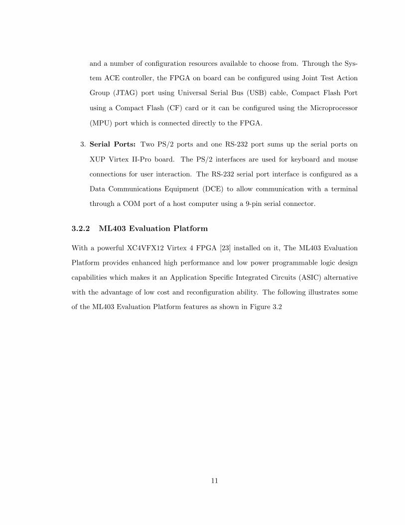
and a number of configuration resources available to choose from. Through the Sys-
tem ACE controller, the FPGA on board can be configured using Joint Test Action
Group (JTAG) port using Universal Serial Bus (USB) cable, Compact Flash Port
using a Compact Flash (CF) card or it can be configured using the Microprocessor
(MPU) port which is connected directly to the FPGA.
3. Serial Ports: Two PS/2 ports and one RS-232 port sums up the serial ports on
XUP Virtex II-Pro board. The PS/2 interfaces are used for keyboard and mouse
connections for user interaction. The RS-232 serial port interface is configured as a
Data Communications Equipment (DCE) to allow communication with a terminal
through a COM port of a host computer using a 9-pin serial connector.
3.2.2 ML403 Evaluation Platform
With a powerful XC4VFX12 Virtex 4 FPGA [23] installed on it, The ML403 Evaluation
Platform provides enhanced high performance and low power programmable logic design
capabilities which makes it an Application Specific Integrated Circuits (ASIC) alternative
with the advantage of low cost and reconfiguration ability. The following illustrates some
of the ML403 Evaluation Platform features as shown in Figure 3.2
11
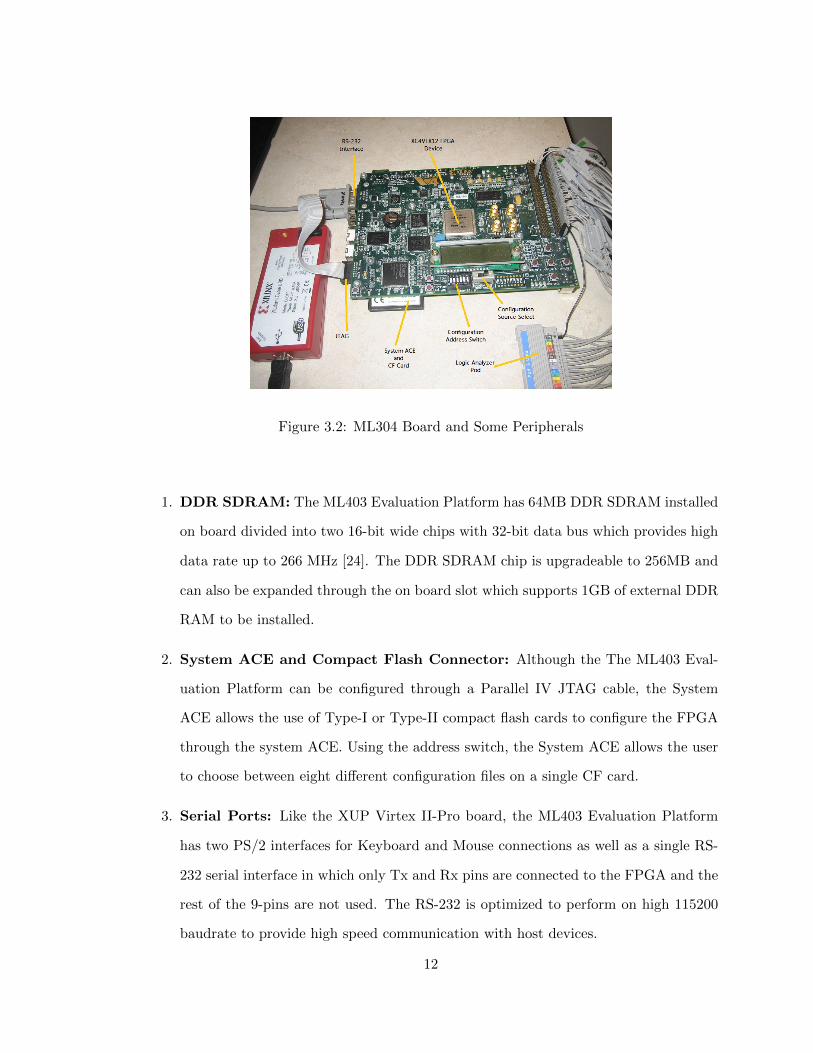
Figure 3.2: ML304 Board and Some Peripherals
1. DDR SDRAM: The ML403 Evaluation Platform has 64MB DDR SDRAM installed
on board divided into two 16-bit wide chips with 32-bit data bus which provides high
data rate up to 266 MHz [24]. The DDR SDRAM chip is upgradeable to 256MB and
can also be expanded through the on board slot which supports 1GB of external DDR
RAM to be installed.
2. System ACE and Compact Flash Connector: Although the The ML403 Eval-
uation Platform can be configured through a Parallel IV JTAG cable, the System
ACE allows the use of Type-I or Type-II compact flash cards to configure the FPGA
through the system ACE. Using the address switch, the System ACE allows the user
to choose between eight different configuration files on a single CF card.
3. Serial Ports: Like the XUP Virtex II-Pro board, the ML403 Evaluation Platform
has two PS/2 interfaces for Keyboard and Mouse connections as well as a single RS-
232 serial interface in which only Tx and Rx pins are connected to the FPGA and the
rest of the 9-pins are not used. The RS-232 is optimized to perform on high 115200
baudrate to provide high speed communication with host devices.
12
3.3 FPGA Architecture
The XC2VP30 and the XC4VFX12 are the two FPGA chips installed on the XUP Virtex II-
Pro and ML403 boards respectively as mentioned in the previous section. In this section we
will discuss the architecture of each of these two FPGA chips and focus on the advantages
that each can provide.
3.3.1 XC2VP30 FPGA
The XC2VP30 is packaged in FF896 BGA package which provides a high capacity of logic
units allowing large area designs to be easily configured on the device [22]. The basic
features of the FPGA are illustrated in the following points.
1. RocketIO MGT cores are parallel-to-serial and serial-to-parallel transceivers used to
provide high bandwidth interconnection between buses and inter-system modules.
RocketIO allows a data rate up to 3.125GB/s to be achieved.
2. Configurable Logic Blocks (CLB) contains the basic combinational and sequential
logic units used for implementing designs. XC2VP30 has 3,424 CLBs each has four
slices giving it a total of 13,696 slices making it easy to fit large area designs with
more place and route options. There are two types of CLBs (F and G) which can be
configured as 4 input Look-Up Tables (LUTs) or 16 bit shift registers.
3. Block RAM memory is cascadable memory which facilitates the implementation of
large embedded storage blocks on the chip with the ability to ”read-during-write”
mode. XC2VP30 offers 2,448 Kb of block RAMs which can be configured in single-
port or dual-port mode with a variety of depth and width settings.
4. Multiplier blocks which are used to perform read, multiplication and accumulation
operations with the available 136 multiplier blocks available. The multiplier blocks
can also be used to implement Digital Signal Processing (DSP) structures.
13

Table 3.1: XC4VFX12 Basic FeaturesFeature Available Resources
CLBs 1,368
Slices 5,472
Logic Units 12,312
Distributed RAM 86
Block RAMs 648 Kb
DCMs 4
PowerPC Cores 1
DSP Slices 32
5. Digital Clock Managers (DCMs), eight available, which provides various functions like
implementing a clock Delay Locked Loop (DLL) that can synchronize different input
clocks to the same design. DCMs can also be used to implement Digital Frequency
Synthesizer (DFS) which provides a multiple or division of input clock or they can
also be used to implement a Digital Phase Shifter (DPS).
6. PowerPC 405 (PPC405) Processor block is the on-chip embedded core for embed-
ded systems implementations. There are two available PPC405 blocks for dual-core
implementations. The structure of PPC405 will be discussed in details in the next
chapter.
3.3.2 XC4VFX12 FPGA
The XC4VFX12 is produced on CMOS 90nm copper process technology based on enhanced
basic blocks from Virtex- II and Virtex-II Pro FPGAs making it up to 40% faster than
previous Virtex generations [25]. Packaged in FF668 package, XC4VFX12 provides 320
I/Os giving designers freedom in design interface choices. The basic features of the FPGA
are shown in Table 3.1.
Since Virtex-4 is based on Virtex-II and Virtex-II Pro, the XC4VFX12 FPGA has the
same features as XC2VP30 with some differences in numbers and sizes of the available
resources. The basic features are shown in the following table
14

DSP slices can perform all operations performed by the multiplier blocks found in Virtex-
II Pro FPGAs with up to 100 % in speed improvement over previous generation devices.
They also provide more efficient implementation of DSP structures using dedicated DSP
units with the option of using pipeline stages.
3.4 Configuration
Both XUP Virtex II-Pro and ML403 platforms provide several configuration options to the
FPGAs installed on them using on-board jumpers and switch settings. We will discuss the
settings for each board and configuration options bellow.
3.4.1 XUP Virtex-II-Pro Configuration
The XUP Virtex II-Pro board can be configured internally using the on-board Platform
Flash configuration PROM or externally using other JTAG configuration options. There
are two settings for the PROM configuration control switch, which if set to on, allows the
PROM to configure the FPGA directly with a pre-configured Xilinx test configuration and
if set to off, the PROM programs the FPGA using user configuration which must be already
programmed on the on-board Platform Flash configuration PROM using one of the external
configuration options.
Configuring the FPGA externally is done through JTAG which supports three different
methods
1. The Compact Flash (CF) card which can hold up to eight configuration files and using
configuration DIP switches, the desired configuration file can be selected.
2. The Parallel Cable IV (PC4) is connected on board through the JTAG configuration
port which can also be used for hardware debugging.
3. The USB to PC connection which allows bitstreams created by programming tools to
be downloaded to the FPGA through embedded Platform cable USB interface.
15

3.4.2 ML403 Configuration
Through the configuration source selector, users can choose between four different methods
to configure the FPGA installed on the ML403 board. Like the Virtex-II Pro Platform, the
ML403 board supports the CF card and Parallel Cable IV JTAG configuration methods
controlled by the system ACE controller. The other two configuration methods are
1. The Platform Flash memory which can hold up to four configuration images selectable
through the configuration address DIP switches. The Platform Flash memory can con-
figure the FPGA with bitstreams in four different modes selectable through iMPACT
programming tools.
2. The Linear Flash which is capable of holding up to eight configuration images that
can be used to configure the FPGA if read by the on-board CPLD in the JTAG chain.
3.5 Tools
Most of the steps in FPGA implementation are done by using CAD tools. From designing
the system using HDL to adding peripherals to running place and route for a desired device,
all is performed by different designing tools. In this section we will be discussing different
tools that were used during the research and their role in building the system.
3.5.1 Xilinx Embedded Development Kit (EDK)
Xilinx Embedded Development Kit (EDK) is a design suite of hardware tools, software
tools and Intellectual Property (IP) which work together to develop a complete embedded
processor SoC to be implemented on programmable platforms and devices [26]. EDK fa-
cilitates, for the designer, the development of the hardware part along with the software
portion of an embedded system through tools offered by the kit which we will illustrate in
the following points.
1. Xilinx Platform Studio (XPS): Using either the command line or the GUI, XPS
16
is used to design the hardware portion of the embedded processor system. The GUI
has a wizard called the Base System Builder (BSB) which allows users to choose the
processor they want to use in the system, clock and reference speeds, memory and
IP cores and it creates the Microprocessor Hardware System (MHS) file according to
the chosen options. The MHS file contains the hardware properties of the system and
it can be edited by the user to change peripherals options and memory allocations.
XPS also allows users to choose the bus type and connection interface between the
embedded processor and the system peripherals along with the ability of connecting
different bus types through bus bridges. Each peripheral in the system has an allocated
address space depending on its size. XPS can generate the beginning and the ending
of this address space automatically or the user can specify their own address space or
modify the generated one by modifying the MHS file.
2. Software Development Kit (SDK): Although XPS can be used to implement
the software portion of the embedded processor system, EDK has a supplementary
tool dedicated for that purpose known as the SDK. Based on the open source tool
Eclipse, SDK provides a software development environment for the embedded sys-
tem by compiling the Microprocessor Software System (MSS) file, which contains the
software description of the system peripherals, along with a C/C++ source code and
peripherals drivers to create an Executable and Linker Format (ELF) file which when
combined with the hardware implementation files, they create the bitstream config-
uration used to configure the board with the embedded system configurations. SDK
is also used for debugging the software portion of the system by communicating with
the system processor through the Xilinx Microprocessor Debugger (XMD) interface.
3.5.2 Xilinx Integrated Software Environment (ISE)
Xilinx Integrated Software Environment (ISE) is a collection of software utilities that fa-
cilitates FPGA design and implementation procedure all integrated in a single tool. ISE
provides utilities for design entry, design verification, synthesis, timing analysis, on-chip
17

place and route and programming target devices. Design entry in ISE can be done through
an schematic editor or by writing Hardware Description Language (HDL) codes using Ver-
ilog or VHDL programming languages. Design verification is provided by running behavioral
or function simulation through supported simulation tools.ISE has the option to optimize
designs for area or speed depending on user choices when synthesizing a design and the tar-
get device. Although an embedded processor system can be created and implemented using
only EDK, it still needs to call the synthesis libraries from ISE to synthesis and implement
the design or to simulate it for verification.
3.5.3 PlanAhead
PlanAhead is a Xilinx software tool used for design analysis and floorplanning. The role
of PlanAhead in Xilinx FPGA design flow, comes after synthesis and netlists are generated
[27]. If a design synthesis and implementation processes were completed in ISE, PlanAhead
can be used to analyze the implementation results, performs time analyses and checks for
better implementation strategy for the target device if available. Like the FPGA Editor
tool, PlanAhead can be used for floorplanning which allows designers to manually place de-
sign components after synthesis then the tool can check afterwards for timing constrains and
design rules violations. It also issues warnings when not using the best available resources
in the target device as well as recommending the best available resources and strategy to
implement the design. PlanAhead can perform Translate and Place-and-Route of a synthe-
sized design to generate a configuration file. It can also be used to perform floorplanning
for partially reconfigurable designs where static and dynamic regions of the design can be
defined and DCM and other resources are implemented accordingly on the target device
[28].
18

3.6 Partial Reconfiguration
3.6.1 Introduction
FPGA is a reconfigurable platform where it can be configured and reconfigured by designers
through an implementation process from writing the design specifications using HDL codes
to generating and downloading the bitstream that is used to configure the FPGA. Each
time an FPGA device is being configured, it requires erasing the previous configuration or
overwriting it completely with the new configuration bitstream and the whole device is on
halt until the new configuration is completely downloaded. As mentioned before, Partial
Reconfiguration (PR) is a method of reconfiguring part of the FPGA device while the rest of
the device is up and running without getting affected by the downloaded partial bitstream
configuration. The main advantages of using partial reconfiguration is that it allows for
more logic to fit into an existing device by making the modules in the design partially
reconfigurable and swapping between them as needed, and having the flexibility in adding
more options to the design modules without the need to re-run Place-and-Route.
Partial reconfiguration method is independent of its implementation method meaning
that although the idea of creating a partially reconfigurable designs is one, different compa-
nies and PLD manufacturers like Xilinx, Altera and Actel have their own tools and imple-
mentation methods to create such designs that differ from one another. Xilinx initially in-
troduced two methods for partial reconfiguration on their devices known as Difference-Base
Partial Reconfiguration and Module-Base Partial Reconfiguration [29]. The Difference-Base
is a simple method used for small designs where the partial bitstream includes only infor-
mation about differences between currently running design and the modifications that were
made hence the name. Modifying Difference-Base designs is mainly done by changing the
LUT equations. Module-Base partial reconfiguration divides the design into base or static
region and partial reconfigurable region, the static region holds the part of the design that
will not be replaced at anytime partial reconfiguration of the device takes place. The partial
reconfigurable region is composed of one or more partial reconfigurable modules in which
19

the portion of the design which will be dynamically partially reconfigured resides. Both
methods are almost neither used by designers nor supported by Xilinx, instead Xilinx in-
troduced Early Access Partial Reconfiguration method to replace both methods with added
benefits and simplicity to partial reconfiguration process flow.
3.6.2 Early Access Partial Reconfiguration
Early Access Partial Reconfiguration (EA PR) method is based on Module-Base Partial
Reconfiguration in the sense that the design is divided into Base Region (BR) which is the
static part of the design and Partial Reconfigurable Region (PRR) which is the dynamic
part of the system composed of Partial Reconfigurable Modules (PRM) that can be swapped
on the fly while the static part of the chip is operational. It is also based on Difference-Base
Partial Reconfiguration in the sense that the partial bitstream modifies the configuration
memory which includes modifying LUT equations as well as other aspects of user design.
EA PR has seven steps to complete the design flow which we will illustrate in the following
points
1. HDL Design Description and Synthesis: A Partially Reconfigurable design must
first be described using either VHDL or Verilog languages and the design should
be in a specific hierarchical manner which includes all static designs, known as the
Base Design Modules (BDM), all Partially reconfigurable designs, known as Partial
Reconfigurable Modules (PRM), and a system design which is the top-level module.
The system design contains I/O of the entire design, global clock, DCMs, BUFGs and
Bus Macro instantiations. Also all the BDMs and PRMs in the design are instantiated
in the top level as black-box instantiations. BDMs represents the static portion of
the system and it cannot contain any clock primitives and also I/O buffers should
be disabled in the synthesis tools. Like BDMs, PRM cannot have BUFGs or DCMs
or any other clock primitive instantiations and Each PRR should have at least one
and usually multiple PRMs associated with that particular PRR and they should all
have the same interface description and port definition. After the design description
20

is fulfilled, each of the modules is synthesized separately and the output is used in the
implementation process.
2. Set Design Constraints: After the previously mentioned design description and
synthesis is done, after synthesis (.ngc) files are generated which can be used to
start the place-and-route process [30]. In addition to timing constraints that any de-
sign flow should follow, PR designs should follow additional area specific constraints
known as Area Group (AG), Area Group Range (AR range), Mode and Location
(LOC)constraints. AG constraints groups the BR logic and each PRR logic in the
system separately to prevent them from merging during implementation. AG range
constraints defines the shape and the area for each PRR in the design where the logic
associated with that specific PRR and its PRMs are placed. The PRR defined by
AG range has a rectangular shape and must include all the BRAMs that fall within
the defined area. The mode constraint prevents NGDBUILD from failing with un-
expanded block errors during base and PR module implementation. LOC constrains
defines the global system logic (DCM, BUFG ... etc.) and bus macros placements.
All these constraints can be defined manually by the user or by using PlanAhead to
perform design floorplanning.
3. Implement the Non-PR Design: Although it is not required, it is recommended
that a design should be synthesized, placed-and-routed and implemented as a non-PR
design before implementing it with PR flow. The purpose of this is to make sure that
the design is bug free and if not, it will simplify the design debugging and aids in
determining the best AG constraints and bus macros placement.
4. Timing/Placement Analysis: After implementing the non-PR design, analyzing
timing and placement of the logic is a very important step as it would reveal whether
the PR region fulfills different constraints requirements and if the bus macros are
placed correctly and do not violate any required conditions.
21

5. Implement the Base Design: If timing and placement analysis is successful, im-
plementing the base design takes place. For successful implementation of the base
design, after synthesis (.nmc) files for the bus macros instantiated in the design top
level should be placed in the same folder as the base design. After implementation,
the usual after place-and-route(.ncd) file is generated for the base design as well as
static.used file which contains routing information of the static portion of the system
to avoid using the same routs by the PRMs.
6. Implement PR Modules: Each PRM in the design should be implemented sepa-
rately in its own folder and the generated static.used file from implementing the base
design should be copied from the base folder to all other PRMs being implemented
so that the routes used by the base design can be excluded from route choices when
implementing PRMs. Also like base designs, PRMs require after synthesis (.nmc) files
for bus macros to be included in each PRM folder, otherwise the NGDBuild step will
fail.
7. Merge: The final step in EA PR flow is the merge step in which the base design and
PRMs are being merged together to create a complete design and partial bitstreams.
The completed design chooses the base design along with one of the PRMs to make the
initial configuration bitstream file for the system and partial bitstreams are created
for each PRM to be used during partial reconfiguration of the system.
All the previously mentioned steps can be done manually by the user by editing con-
straint files in ISE or by using PlanAhead which can simplify some of the steps by checking
for violations in the constraints automatically and pointing them out to be fixed.
3.6.3 Internal Configuration Access Port
We have already discussed some of the methods that can be used to configure the FPGA
which require an external source (Like PC or CF card) to load configuration bitstreams.
The Internal Configuration Access Port (ICAP) gives the user design the ability to write
22

the configuration memory during run-time. Initially, The FPGA has to be externally con-
figured with a complete design then ICAP can be used to reconfigure some portions of the
FPGA. In embedded systems, the designer writes software programs which compiles to the
microprocessor op-code instructions, these software instructions enables the microprocessor
to read and write the configuration memory through ICAP. Modifying a design using ICAP
is done with a technique known as read-modify-write mechanism where the portion of the
system that needs to be modified is read in frames, one at a time, and stored in a BRAM.
After all the frames have been read and stored in the BRAM, necessary modifications take
place and the modified frames gets written back through ICAP same way they were read
(i.e. one frame at a time) as shown in Figure 3.3.O
PB
Bus
EmbeddedProcessor
ICAP
HWICAP
Dual−Port
BRAM
FPGAConfiguration
Memory
Figure 3.3: ICAP Configuration Process
In Early Access Partial Reconfiguration, ICAP is used in the same way as described
except that the modifications that needs to be done are in the form of partial bitsreams
that resides in an external memory source (i.e. CF Card) but the difference between loading
the data into configuration memory from an external source through ICAP and through any
other configuration source (i.e. JTAG) is that ICAP only affects the portion of the design
23

that it being modified or swapped through partial reconfiguration without interrupting
the remaining of the design while other configuration sources affect the whole chip and
reconfigures the design completely.
3.6.4 Bus Macros
Because it is forbidden ,in partial reconfiguration, for static regions and partially reconfig-
urable regions to overlap and the routes used by the BDM cannot be used by PRMs, Early
Access Partial Reconfiguration provides a component that allows communication between
BDM and PRMs known as Bus Macros (BM) [30].Bus macros provide a mean of locking
the routing between PRMs and the BDM, making PRMs pin compatible with the base
design as shown in Figure 3.4. With the exception of global clock signals, all other signals
including reset signals must pass through BMs when communications between BDMs and
PRMs occur.
Bus Macros
PRR1PRR2
Static Region
FPGA
Figure 3.4: Bus Macros Used to Lock Routing Between PRMs and BDM
All BMs has a bandwidth of 8-bit and provide enable/disable control but there are three
main factors that defines and differentiates between Bus Macros as provided by Xilinx
1. Signal Direction: As stated, communication between BDMs to PRMs is usually
24
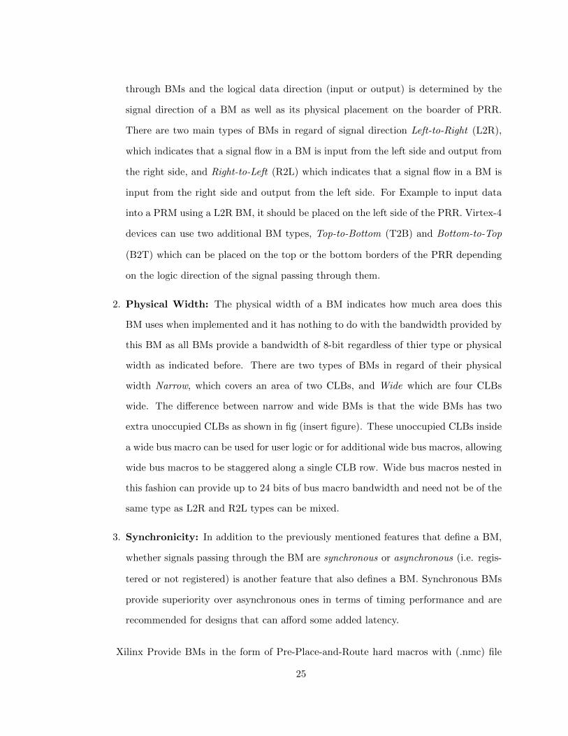
through BMs and the logical data direction (input or output) is determined by the
signal direction of a BM as well as its physical placement on the boarder of PRR.
There are two main types of BMs in regard of signal direction Left-to-Right (L2R),
which indicates that a signal flow in a BM is input from the left side and output from
the right side, and Right-to-Left (R2L) which indicates that a signal flow in a BM is
input from the right side and output from the left side. For Example to input data
into a PRM using a L2R BM, it should be placed on the left side of the PRR. Virtex-4
devices can use two additional BM types, Top-to-Bottom (T2B) and Bottom-to-Top
(B2T) which can be placed on the top or the bottom borders of the PRR depending
on the logic direction of the signal passing through them.
2. Physical Width: The physical width of a BM indicates how much area does this
BM uses when implemented and it has nothing to do with the bandwidth provided by
this BM as all BMs provide a bandwidth of 8-bit regardless of thier type or physical
width as indicated before. There are two types of BMs in regard of their physical
width Narrow, which covers an area of two CLBs, and Wide which are four CLBs
wide. The difference between narrow and wide BMs is that the wide BMs has two
extra unoccupied CLBs as shown in fig (insert figure). These unoccupied CLBs inside
a wide bus macro can be used for user logic or for additional wide bus macros, allowing
wide bus macros to be staggered along a single CLB row. Wide bus macros nested in
this fashion can provide up to 24 bits of bus macro bandwidth and need not be of the
same type as L2R and R2L types can be mixed.
3. Synchronicity: In addition to the previously mentioned features that define a BM,
whether signals passing through the BM are synchronous or asynchronous (i.e. regis-
tered or not registered) is another feature that also defines a BM. Synchronous BMs
provide superiority over asynchronous ones in terms of timing performance and are
recommended for designs that can afford some added latency.
Xilinx Provide BMs in the form of Pre-Place-and-Route hard macros with (.nmc) file
25

extension. The naming convention that Xilinx uses and recommends for BMs includes all the
previously mentioned properties. For Example, the BM busmacro xc2vp l2r async narrow.nmc
is Left-to-Right in direction, its physical width is Wide and asynchronous [30]. It can also
be noticed from the name that it can be used with Virtex II Pro devices.
26

Chapter 4: Implementation Methodology
4.1 Overview
Reconfigurable Platforms like FPGA chips provide hardware solutions that allow the end
product to perform at high speeds that cannot be established through software solutions.
But regardless of the amount of logic that you can have on an FPGA chip, it will always
be limited resources and this is why efficiency in performance is usually measured by a
combination of area and speed. This limitation in resources can be a problem when designing
for hardware depending on the area consumed by a design and the amount of resources
available on the target device on which the design will reside.
Partial Reconfiguration provides a solution for this problem as it can make use of the
same area and resources to be used by different modules in the design without affecting other
modules or their functionality. The idea is to find modules in the design that are not used
all the time when the device is functional and implement them as reconfigurable modules so
that they would be swapped with each other when requested. Not only that implementing
the design in a reconfigurable fashion makes use of the available area efficiently, but it also
produces more power efficient design implementations [5] as power consumption increases
with the increase in area making this method suitable for light-weight implementations
targeting low area devices which are powered by limited energy and power resources and
should be very efficient in power and energy consumption.
We have built a system that makes use of partial reconfiguration and its benefits which
is capable of performing IPSEC operations using reconfigurable modules. In addition to
the previously mentioned advantages, implementing IPSEC using partial reconfiguration
provides flexibility in the choices of algorithms or protocols available to an application as
not all applications require all the operations that IPSEC offers. Within this system, we
27

also implemented an embedded processor which is considered to be the static portion in the
system along with its supporting peripherals to controls the reconfiguration procedure of
the reconfigurable modules. The benefit of using an embedded processor can be summarized
in the following point:
• It makes the system more autonomous as it is capable of self-reconfiguring the partial
reconfigurable regions with modules requested by an application being processed.
• It allows faster response to changes happening in the system.
• It adds flexibility to the system by providing control over the system through software
instructions using C language.
• Adding an embedded processor to the implementation could be free if the hard core
embedded processor is used as it exists on the FPGA device anyway.
In the following sections, we will be discussing all modules in the system, their design
descriptions and how they were integrated in the system.
4.2 Design Description Overview
As mentioned, the system is composed of static regions ,which include an embedded proces-
sor and some supporting peripherals, and reconfigurable regions, which include the recon-
figurable modules of the IPSEC protocol. The design targeted two platforms, the Virtex-II
Pro and the Virtex-4 devices described in the previous chapter along with their development
boards. As both devices contain an embedded hard core PowerPC 405 processor, both the
soft core (Microblaze) and hard core processors were used in different versions of the design.
28

Bridge
PowerPC/MicroblazePLBPLB
OPB
System ACE
UARTICAP
BRAMCNTRL BRAM
DCRSocket
OPB2DCRBridge
CF
EnableBM
PRR
PLB2OPB
Figure 4.1: Embedded System Processor and Peripherals
The processor is connected to the BRAM-block peripheral through the Processor Lo-
cal Bus (PLB) BRAM Interface Controller (BRAM IF Ctrl) which is interfaced as a Slave
to the PLB Bus As shown in Figure 4.1. The BRAM-block peripheral gives the processor
access to the BRAM components allowing data and instructions to be stored. The peripher-
als in the system are interfaced to the system through The On-chip Peripheral Bus (OPB)
as Slave to the OPB. The peripherals in the system includes a Universal Asynchronous
Receiver/Transmitter (UART), a System ACE and HWICAP. There is also a custom pe-
ripheral which represents the Partial Reconfigurable Region in the system that holds the
Reconfigurable Modules. This custom peripheral is interfaced to the system through the De-
vice Control Register (DCR) bus. There are also two bus bridges used, the plb2Opb bridge
and opb2dcr bridge, to allow the communication between different buses in the system and
the peripherals interfaced to them. This is a brief description of the system as it can be
seen in Figure 4.1 and in the following sections we will be discussing the processors, buses
and each peripheral in the system with more details.
29

4.3 Hardware Architecture
4.3.1 Processor Cores and Buses
The basic components that define an embedded system are the microprocessor that con-
trols the system and the buses on which data and instructions can be transfered from the
microprocessor to other components and peripherals in the system. In this section we will
describe the two processors which were used in different versions of our design and the buses
associated with them.
PowerPC and Microblaze
In EDK, Xilinx offers two microprocessors to be used in embedded system designs PowerPC
and Microblaze [31]. The PowerPC 405 (PPC405) is an embedded 32-bit hard core processor
that was introduced by IBM to fit inside specialized applications like FPGA devices. The
PPC405 can be found in the Virtex-II Pro and Virtex-4 FPGA devices. The main features
of PPC405 can be summarized in the following points:
• A 32-bit Reduced Instruction Set Computer (RISC) processor core which has a 64-
bit architecture with 32-bit subset but only 32-bit implementations are included in
embedded designing environments like EDK.
• It uses IBM User Instruction Set Architecture (UISA) for embedded environment.
• There are thirty two 32-bit General Purpose Registers (GPRs) for data and address
operations.
• Five-stage pipeline with single-cycle execution of most instructions, including loads
and stores.
• Two 16K 2-way set associative cache memories, instruction cache and data cache with
eight words per cache line in each.
30

• Supports hardware debugging through forward and backward instruction tracing using
Xilinx Microprocessor Debugger(XMD) and JTAG
• A Memory Management Unit (MMU) provides address translation, protection func-
tions, and control for memory access.
Microblaze is an embedded 32-bit soft core processor introduced by Xilinx specifically for
Xilinx FPGA devices. It can be implemented on any Xilinx FPGA device that can fit its
size unlike PowerPC which can only be found in some of the Virtex devices. The main
features of the Microblaze processor are:
• It is a 32-bit RISC-based processor core with few optimizations made by Xilinx for
its FPGA implementations
• It has thirty two 32-bit GPRs to perform data and address operations
• Two different pipelining are supported, 3-stage and 5-stage single issue pipeline
• 32-bit instruction word with three operands and two addressing modes
• Optional direct mapped data and instruction cache memory
• Contains a MMU that was implemented based on PowerPC MMU architecture.
The advantages of using PPC405 is fast and has dedicated cache units and does not add
overhead to the the design area consumption as it is already embedded in the FPGA but
the disadvantage is that it is only implemented on few Xilinx devices where as Microblaze
can be implemented in any FPGA device as long as it can fit its logic but the disadvantages
is that it adds to the design area overhead.
Core Bus Architecture
The IBM CoreConnect bus architecture simplifies the integration and reuse of the processor
system and peripheral cores within standard product and custom SoC designs [32]. This
bus architecture includes three bus implementations
31

• Processor Local Bus (PLB): With 64-bit data width, the Xilinx PLB Version 3.4
consists of a bus control unit, a watchdog timer, and separate address, write, and
read data path units with a a three-cycle only arbitration feature [33]. It is fully
synchronous and supports 64/32-bit data transfer. It is mainly used to interface high
speed peripherals and peripherals that are local to the processor like the instruction
and data cache. Peripherals can be interfaced to the PLB bus through Master PLB
(MPLB) interface or Slave PLB (SPLB) interface.
• On-chip Peripheral Bus (OPB): The OPB version 2.0 is a full-featured bus architecture
with many features that increase bus performance [34]. It is fully synchronous and
supports 32-bit data. It is used to interface different peripherals in the system with
the processor and with each other by providing Master and Slave interface options
to the bus (MOPB and SOPB). Although the OPB is not as fast as PLB, it can
still be interfaced with it through a plb2opb bridge which allows the processor to
communicate with the peripherals interfaced with the OPB.
• Device Control Register (DCR): The 32-bit wide DCR bus version 2.9 provides fully
synchronous movement of GPR data between CPU and slave logic [35]. It provides
the daisy-chain for the DCR data bus which allows the a single master to be directly
connected to a number of slaves on the bus. The DCR has another important feature
related to PR in which it interfaces the dcr socket to the OPB. The dcr socket disables
bus macros during partial reconfiguration to prevent communication between the PRR
and other Peripherals in the system until the new RM is completely configured. It can
be interfaced with OPB bus through opb2dcr bridge to allow communication between
peripherals interfaced to it and the processor and other peripherals in the system.
32

AES and SHA2 Cores
The PRR represents the peripheral in the system that is responsible for performing the
functionality of the IPsec Protocol. As we discussed before, the protocol performs differ-
ent functionality depending on the application being processed and the security service it
demands. For example, if the application requires confidentiality then the data in the appli-
cation should be encrypted to assure confidentiality and if the application requires integrity
then a hash value is calculated from the application data using a hash function and send it
with the original data. For these security services to be provided, the IPsec uses a number
of cryptographic algorithms like the Advanced Encryption Standard (AES) with 128-bit
key which assures confidentiality is provided by the system and Hash-Message Authenti-
cation Code with Secure Hash Algorithm 256 (HMAC-SHA-256) to assure data integrity
and authentication are provided by the system. The AES is a symmetric key cipher which
uses the same key for encryption and decryption. There are four main operations that
take place during encryption of a data and the inverse of these operations is used during
decryption.These four operations as described in [36] are as follows:
1. SubBytes: The subBytes transformation is a non-linear byte substitution that oper-
ates independently on each byte of the State using a substitution table (S-box).
2. ShiftRows: In this transformation, the bytes in the last three rows of the State are
cyclically shifted over different numbers of bytes (offsets).
3. MixColumns: The MixColumns transformation is a mixing operation which operates
on the columns of the state, combining the four bytes in each column.
4. AddRoundKey: In the AddRoundKey transformation, a Round Key is added to the
State by a simple bitwise XOR operation.
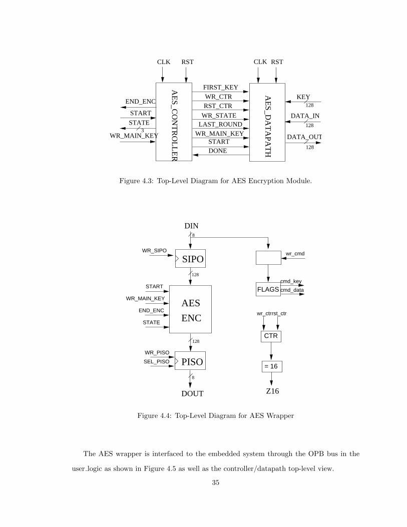
We implemented the AES core in hardware as a RM in the PRR region that represents the
hardware accelerator for the IPsec protocol in the system. The datapath for AES encryp-
tion module is 128-bits as shown in Figure 4.2. The state register is also used for debugging
33

purposes during the hardware/software synchronization to determine the current state of
AES. Figure 4.3 shows the top-level view for the datapath/controller signal communication
along with the interface with the design top-level.
output
=
wr_ctrrst_ctr
CTRRD_num
done
input
KEY GEN
wr_keyfirst_key
RD_keyAES_ROUND
STATE REGISTERwr_state
first_key
last_round
10
128
128 4
128
128
128
128
128
128
key
Figure 4.2: AES DataPath.
On top of the AES datapath, we created a wrapper to give the datapath an 8-bit interface
through Single Input/ Parallel Output (SIPO) for the input data and Parallel input/ Single
output (PISO) for the output as shown in Figure 4.4. It is also used to interpret whether the
input is actual data or key depending on the command send before the data to wr cmd. The
input is interpreted as key if the value 0x40 was sent before the input and it is interpreted
as data if it was preceded by the value 0x80.
34
128
WR_CTRRST_CTR
CLK RST CLK RST
FIRST_KEY
WR_STATELAST_ROUND
WR_MAIN_KEYSTARTDONE
AE
S_CO
NT
RO
LL
ER
AE
S_DA
TA
PAT
HDATA_OUT
DATA_IN
KEY
START
WR_MAIN_KEY
STATE3
END_ENC
128
128
Figure 4.3: Top-Level Diagram for AES Encryption Module.
Z16
SIPOWR_SIPO
= 16
START
WR_MAIN_KEY
END_ENC
STATE
AES
ENC
DIN
DOUT
wr_ctrrst_ctr
CTR
FLAGScmd_key
wr_cmd
cmd_data
PISOWR_PISO
SEL_PISO
128
8
128
8
Figure 4.4: Top-Level Diagram for AES Wrapper
The AES wrapper is interfaced to the embedded system through the OPB bus in the
user logic as shown in Figure 4.5 as well as the controller/datapath top-level view.
35

DATA_OUT
WR_CTR
Z16
RST_CTR
WR_CMDCMD_DATA
CMD_KEYWR_MAIN_KEY
STARTEND_ENCWR_SIPO
WR_PISOSEL_PISO
AE
S_WR
AP_E
NC
_CT
RL
DA
TA
PAT
H
CLK RST CLK RST
STATE
SRC_READY
SRC_READ
3 5
8
DST_READY
DST_WRITE
DATA_IN
Figure 4.5: AES Wrapper
The HMAC is a combination of Message Authentication Code (MAC) and a hash func-
tion to ensure data integrity and authenticity of a message, it is also known as keyed hash
functions [37] as they perform all hash function operations but they also use a key to assure
authentication. The HMAC operates in the following way:
1. The key is added to a known value specified in [37] HMAC standard known as I-PAD
using simple bitwise XOR operation.
2. The output I-KEY-PAD from the previous step is padded with the message and input
to the hash function
3. The key is also added to another constant value specified in [37] known as O-PAD in
the same way as step one
4. The output O-KEY-PAD from step 3 is padded with the hash value calculated in step
2 and the padded value is input again to the hash function
36

5. The output from the hash function is the calculated HMAC value.
SHA−512: All buses are 64−bit wide with z = 512
F =Gt+1
Ht+1
Ht+1
Wt+1
t+1KCSA
CSA
CSA
SE t
CE t
CA t
SA t
FttG
EtFt
AtBt
BtCt
CtDt
Dt
Ft
Ch
tG
Σ1
Et
+Et+1 Et
+
Ft
Ch
tG
Σ1
Et
+
MajΣ0
Bt CttA
t+1A tA +
HH
HG
HF
HE
HD
HB
HA
HC
PIS
O
B
C
D
H
G
F
HGHH
A
E
Reset
0
0
HA
HE
HB’
HC
HD
HF’
HG
HF’
HB’
SE
CE
SA
CAz dout
t
Figure 4.6: SHA-256 Datapath
Due to the fact that any hash functions can be used to calculate HMAC value, The
hash function that is being used to calculate a HMAC value should be added to the HMAC
name i.e. HMAC-MD5 indicates that MD5 hash function is being used to perform HMAC
calculations. As IPsec protocol supports different hash functions to be used for HMAC
calculation, Secure Hash Algorithm 256 (SHA-256) is the hash function we used for HMAC
calculations. Figure 4.6 illustrates the SHA-256 datapath we implemented to be used as
another RM in the PRR region to perform the hash function operations to calculate HMAC
as a service provided by the IPsec protocol. The datapath is 256-bit with a 32-bit interface
to the datapath wrapper through PISO similar to AES. The datapath wrapper shown in
Figure 4.7 uses SIPO and PISO to interface the 32-bit output from the datapath to the
common interface it shares with AES. The top-level for the SHA-256 Wrapper shown in
37

Figure 4.8(controller/datapath) has the exact same interface as the AES as so that they
can share the same PRR.
PISO
SIPO
KW_WR
WR_DATA
WR_RESULT
WR_STATE
WR_LEN
SEL
SEL2
SEL_GH
SEL_GH2
CTR_ENA
Z16
ZLAST
SKIP_WORD
08
DST_WRITE
WR_LB WR_MB
RST_FLAGS
WR_CNCTR
LAST_BLOCK
MSG_DONE
UPDATE_RESULT
WR_PISO
SEL_PISO
8
8
8
32
WR_SIPO
DIN
RS
_DA
TA
PA
TH
Figure 4.7: SHA-256 Datapath
CMD_CON
SEL_PISO
WR_PISO
CMD_INIT
CMD_READ
WR_SIP0
RST_CTR
WR_CTR
WR_CMD
24
WR_STATE
WR_RESULT
WR_DATA
KW_WR
WR_LEN
SEL
SEL2
SEL_GH
SEL_GH2
CTR_ENA
Z16
ZLAST
SKIP_WORD
08
WR_LB
WR_MD
WR_CNCTR
LAST_BLOCK
RST_FLAG
MSG_DONE
SFT_RESULT
INIT_IV
UPDATE_RESULT
DOUT
DIN8
8SRC_READ
SRC_READY
DST_WRITE
DST_READY
STATE8
SH
A2_W
RA
P_D
P
SH
A2_W
RA
P_C
TR
L
Figure 4.8: SHA-256 Wrapper
38
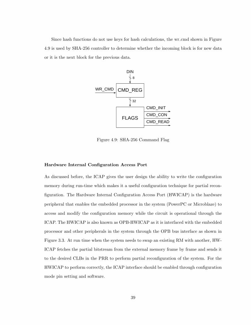
Since hash functions do not use keys for hash calculations, the wr cmd shown in Figure
4.9 is used by SHA-256 controller to determine whether the incoming block is for new data
or it is the next block for the previous data.
CMD_REG
8
32
DIN
WR_CMD
CMD_INIT
CMD_READ
CMD_CONFLAGS
Figure 4.9: SHA-256 Command Flag
Hardware Internal Configuration Access Port
As discussed before, the ICAP gives the user design the ability to write the configuration
memory during run-time which makes it a useful configuration technique for partial recon-
figuration. The Hardware Internal Configuration Access Port (HWICAP) is the hardware
peripheral that enables the embedded processor in the system (PowerPC or Microblaze) to
access and modify the configuration memory while the circuit is operational through the
ICAP. The HWICAP is also known as OPB-HWICAP as it is interfaced with the embedded
processor and other peripherals in the system through the OPB bus interface as shown in
Figure 3.3. At run time when the system needs to swap an existing RM with another, HW-
ICAP fetches the partial bitstream from the external memory frame by frame and sends it
to the desired CLBs in the PRR to perform partial reconfiguration of the system. For the
HWICAP to perform correctly, the ICAP interface should be enabled through configuration
mode pin setting and software.
39
Other Peripherals
In addition to the peripherals mentioned, there are other auxiliary peripherals interfaced to
the system through the OPB Slave interface (SOPB) as follows:
• Universal Asynchronous Receiver/Transmitter: The Recommended Standard 232 (RS232)
is interfaced with the system through opb uartlite peripheral. Using a serial cable
and a PC, the opb uartlite can transfer characters to a standard VT100 terminal (like
HyperTerminal) or communicate with other external devices that has the RS232 inter-
face. Different baudrates are supported by the opb uartlite peripheral in EDK but the
same baudrate should be set for the terminal program as well for data transmission
to be successful.
• System ACE: As mentioned, partial bitstreams that are being used to reconfigure
the PRR with PMs needs to be stored in an external memory. A FAT32 Compact
Flash (CF) memory card is used as the non-volatile memory that holds the partial
bitstreams and it is being interfaced with the system through opb sysace to allow the
loading and swapping between different PMs.
• DCR Socket: The opb dcr socket peripheral plays an important role in a partial
reconfigurable design. It disables the bus macros during partial reconfiguration of the
PRR through ICAP to prevent signal from passing from the static region to the PRR
and the other way around. Without the existence of such mechanism, a successful
partial reconfiguration would not occur.
4.3.2 Software Architecture
Overview
As much as the hardware portion is to an embedded system, the software portion is of equal
importance to the system. In addition to the software drivers for the hardware peripherals
in the system and some basic C libraries, EDK has a GNU Compiler Collection (GCC)
40
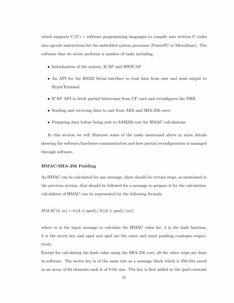
which supports C/C++ software programming languages to compile user written C codes
into opcode instructions for the embedded system processor (PowerPC or Microblaze). The
software that we wrote performs a number of tasks including
• Initialization of the system, ICAP and HWICAP
• An API for the RS232 Serial interface to read data from user and send output to
HyperTerminal
• ICAP API to fetch partial bitstreams from CF card and reconfigures the PRR
• Sending and receiving data to and from AES and SHA-256 cores
• Preparing data before being sent to SAH256 core for HMAC calculations
In this section we will illustrate some of the tasks mentioned above in more details
showing the software/hardware communication and how partial reconfiguration is managed
through software.
HMAC-SHA-256 Padding
As HMAC can be calculated for any message, there should be certain steps, as mentioned in
the previous section, that should be followed for a message to prepare it for the calculation.
calculation of HMAC can be represented by the following formula
HMAC(k,m) = h((k ⊕ opad)//h((k ⊕ ipad)//m))
where m is the input message to calculate the HMAC value for, h is the hash function,
k is the secret key and opad and ipad are the outer and inner padding constants respec-
tively.
Except for calculating the hash value using the SHA-256 core, all the other steps are done
in software. The secret key is of the same size as a message block which is 256-bits saved
in an array of 64 elements each is of 8-bit size. The key is first added to the ipad constant
41

by XOR the the elements of the key array to the ipad constant array. The message block,
which is also 256-bit of size, is concatenated with the padded key and the 512-bit data is
sent to the SHA-256 core 8-bits at a time as this is the interface of the SHA-256 core as
explained in the previous section. The 256-bit hash value output from the SHA-256 core
is then again concatenated with the secret key padded with the opad constant in the same
fashion it was padded with the ipad. The 512-bit data is again being sent 8-bits at a time
and the output from the SHA-256 core is the final HMAC value.
Although all the HMAC steps can be done in hardware, but we chose to do the message and
key input as well as the padding process in software to give our design portability as any
hash function can be used by changing only the hardware core and not limit the calculations
of HMAC to only using SHA-256 core.
ICAP-API
To Allow the embedded processor in the system to perform self partial reconfiguration to
the system without interference from the user to reprogram the PRR with different RM,
an API for the ICAP is needed in software. The ICAP API defines methods for access-
ing configuration logic through the ICAP port. The main methods move data between
the configuration cache (BRAM) and the active configuration memory (the device). Other
methods allow the processor to read and write to the configuration cache [38]. For the ICAP
functions to be included, the xhwicap.h and hwicap cf.h header files must be included in
the source code of the design application.
The HWICAP needs to be initialized using XHwIcap Initialize function set with the follow-
ing parameters as defined in [39]
• InstancePtr: A pointer to the XHwIcap instance to be worked on.
• DeviceId: User defined ID for the instance of this component which in our design is
the name of the hardware instance interfaced to the OPB bus.
• DeviceIdCode: IDCODE of the FPGA device to be used. For our design the constants
42
that were used are XHI XC4VFX12 for the Virtex-4 board and XHI XC2VP30 for
the Virtex-II-Pro board. The constant XHI READ DEVICEID FROM ICAP can be
used instead of specifying the IDCODE directly.
The return value for this function is XST SUCCESS in the case of a successful initial-
ization or XST INVALID PARAM if the parameters were not set correctly or initialization
fails.
The XHwIcap CF2Icap function is used to allow the HWICAP to fetch the partial bit-
streams from the external CF memory card and reconfigure the PRR with a new RM
through ICAP. There are two parameters for this function
• InstancePtr: A pointer to the XHwIcap instance same as with the initialization func-
tion.
• File Name: Which is the partial bitstream stored on the CF memory card in File
Allocation Table 32(FAT32) format.
4.3.3 Hardware-Software Synchronization
Overview
In a hardware/software co-design as in embedded systems, synchronization between the
hardware and software is essential for the system to perform correctly. As the hardware is
much faster than the software, control signals should be added to the hardware to prevent
events from happening before the software is ready thus preventing loss of data. When
using the Base System Builder (BSB) in EDK, all the hardware modules in the system
created have the control signals which assures that the hardware and the software are
in sync. But when adding a custom IP, it is up to the designer to make sure of the
synchronization between the hardware and the software using a certain handshaking or
protocol. In this section we will discuss the protocol we used in our design to provide
synchronization between the hardware and software along with a brief explanation of the
43

interface between the embedded system and the custom IP and the testing and debugging
method we used to make sure that our protocol is working.
Control Signals and FIFO interface
When creating a custom peripheral in EDK, it creates user logic.vhd module to be edit by
the designer to instantiate their own modules. The processor is connected by OPB bus to
other peripherals in the system , so a custom peripheral must be OPB compliant. Meaning
the top-level module of a custom peripheral must contain a set of bus ports that is compliant
to OPB protocol, so that it can be attached to the system OPB bus (maybe a fig). Most of
these signal are being taken care of when creating a custom peripheral using the ”‘Create
Custom Peripheral”‘wizard in EDK, but if the designer is instantiating their own modules
in the user logic, additional control signals are needed to assure the synchronization when
communicating with hardware.
The protocol we offer is composed of four control signals
• src ready: An input signal from the software to the custom peripheral indicating that
the software is ready to send data in
• dst ready: An input signal from the software to the custom peripheral indicating that
the software is ready to receive data out
• src read: An out signal from the custom peripheral to the software indicating that
the custom peripheral is ready to receive data in
• dst write: An out signal from the custom peripheral to the software indicating that
the custom peripheral is ready to send data out
The way it works is simple, For the data to be sent from the software to the hardware,
both src ready and src read signals need to be high for the hardware core to accept a new
input value from the software and both dst ready and dst write signals need to be high
for the software to accept new output data from the hardware. Figure 4.10 shows how the
signals are connected to the hardware and the software. The two flip-flops in the diagram are
44

used to prevent the signals from being high for more than one clock cycle which prevents the
hardware from reading more than one input per clock cycle and from sending more than one
output per clock cycle allowing the software to be ready when data is sent. The write ack
is triggered high when any of the software registers are being written by the software thus
enabling the flip-flops only when the software is sending data to the hardware.
src_ready
src_read
dst_ready
dst_write
data_in data_out
SHA/AES
BUS2IP_rst
FFin out
rst
32
8 1 1
32
8
FFin out
rst
rd_ACK
en
1
1
1
11 1
8 8
wr_ACK
Software Input Register Software Output Register
en
rst
BUS2IP_clk
Figure 4.10: Synchronization Circuit Between Hardware and Software
Another problem this interface solves is that caused by consecutive writing to the OPB
bus which results in a bus freeze that prevents new data from being written to peripherals
attached to it. This method gives the OPB bus enough time in between consecutive writes
to be released thus prevents any bus freeze.
Logic Analyzer
As we encountered some troubles with simulating the system during the design and imple-
mentation phases, we thought of debugging the system at run-time using a logic analyzer.
We created two extra ports in the top level of a non-PR embedded system (for testing
purposes) with both hardware cores (AES and SHA-256) attached to the processor through
OPB and mapped all the input and output signals between both cores and the software to
these ports and mapped these ports to the on-board pins through the User Constraints File
45

(UCF).
Figure 4.11: Logic Analyzer Waveform Triggered at src ready
Using the logic analyzer, we could trigger different events though the software and
capture the activity on the control and data signals as shown in Figures 4.11 and 4.12
which show the behavior of input and output signals respectively at run-time. Not only
that the data that was collected and sampled by the logic analyzer helped us in debugging
the system, it also allowed us to see exactly what is happening in hardware at run-time
which prevented any defects in the system that may not have been detected by simulation.
46
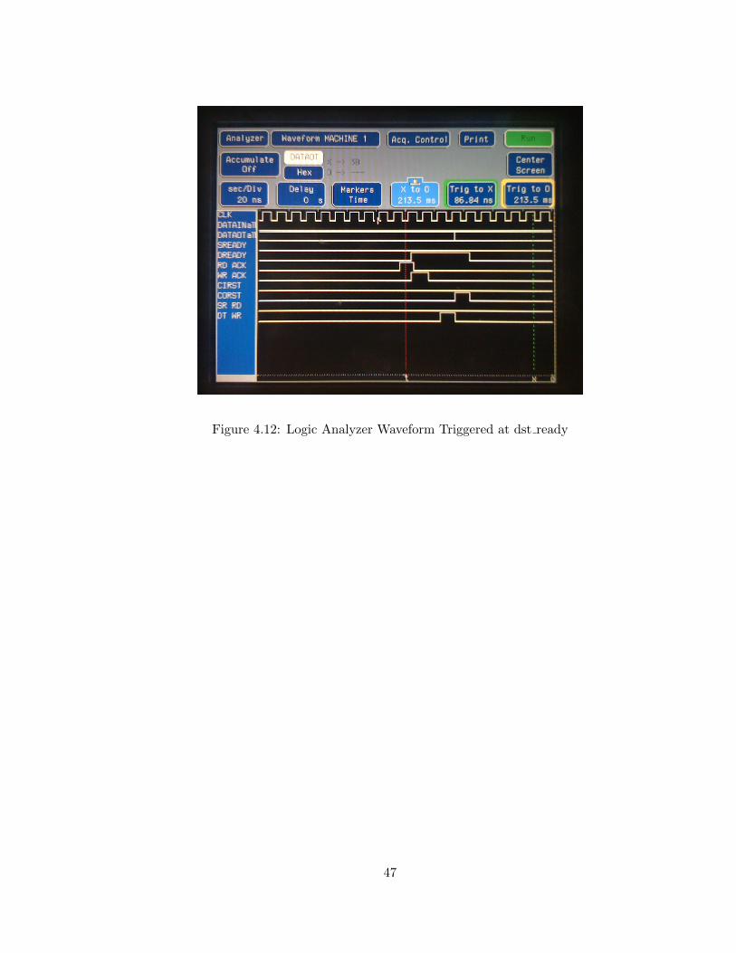
Figure 4.12: Logic Analyzer Waveform Triggered at dst ready
47

Chapter 5: Experiment Methodology
5.1 Overview
To implement the proposed design in a PR system, we needed to implement the design in a
non-PR system for a number of reasons. The main reason was to make sure that the AES
and SHA-256 cores perform as expected and producing the correct results at run-time. We
also wanted to test the hardware/software synchronization using the interface discussed in
the previous chapter. Finally, we wanted to see the amount of area consumed by having
both cores implemented on different regions of the FPGA device in the non-PR design.
After we implemented the non-PR design successfully, we started creating the PR design
by defining the static portion and the dynamic portion which will be the PRR
• Static Portion: This portion of the system includes the embedded processor along
with PLB and OPB buses and the supporting peripherals like the UART and CF
card interfaces
• Dynamic Portion: which includes the modules that can be reconfigured during run-
time which are the AES and SHA-256 cores.
In this chapter we will show the steps for building the PR system according to the
specifications we discussed in previous chapters and discuss the problems we encountered
during different design phases and how we solved them.
5.2 Static Portion Of The System
The first step is to build the processor system using the Base System Builder (BSB) wizard
in EDK which includes the following steps
48

• Select the target board (Virtex-II-PRO and Virtex-4) so that common peripherals can
be loaded by EDK and available to use.
• Select the processor to be used in the design (Microblaze and PowerPC)
• add supporting peripherals to the system which includes a UART for communication
with PC through HyperTerminal, Compact Flash to store partial bitstreams and
HWICAP to load the partial bitstreams from the Compact Flash during run-time
After the system is created, all peripherals are interfaced with the system processor through
the PLB bus and with each other through the OPB bus by default. The DCM clock instance,
also created by default, is deleted from the processor system as partial reconfiguration
requires for clock instances (i.e. DCM) and BUFG to be instantiated only in the top level
and not in the lower level. We also added dcr socket peripheral to disable the bus macros
during partial reconfiguration. The software application is created which includes ICAP
API to allow self partial reconfiguration of the system, HMAC padding function and UART
functions. The last step in creating the static portion is to generate netlist files and build
user applications to generate library files and drivers for the added peripherals.
5.3 Dynamic Portion Of The System
After the base system is defined, custom peripherals are added which represent the recon-
figurable modules in the system. First we create a custom peripheral and interface it to the
OPB bus using the IP interface (IPIF) with the support of two software registers to allow
communication between the software and the custom hardware core.
Once the peripheral is created, modifications to user logic.vhd generated for the custom
peripheral are made by instantiating the top-level Of the AES module and adding the
hardware/software synchronization circuit that was described in chapter four. the lower
level files of the AES module are added to the Peripheral Analysis Order (PAO) file in
hierarchical order to be included during the design synthesis phase.
The same process is repeated again to create a peripheral for the SHA-256 module.
49
5.4 Design Synthesis and Top-Level creation
Although EDK is capable of running synthesis for embedded system designs, partially re-
configurable designs required to be synthesized using a modified version of ISE that follows
the design rules for EA PR mentioned in chapter three. Each of the custom peripheral
created are imported to ISE to be synthesized to generate after synthesis .ngc files. During
synthesis I/O buffer insertion should be disabled as these are lower level modules.
The Top-Level for the design is then created in a separate ISE project. It includes
instantiations of the the two custom peripherals (AES and SHA-256) as black boxes, in-
stantiation of the embedded system, adding the system.xmp file to the project which holds
the information of the embedded system and bus macros instantiations to allow routing of
data between the base system and the RMs. Also DCM and BUFG instances are added to
the top-level before it is synthesized to generate the after synthesis .ngc file.
5.5 Design Floorplanning and Implementation
Now the design is ready to be floorplanned, and for this, a new project is created in PlanA-
head and .ngc files for top-level, SHA-256 and bus macros are added to the project to load
the netlists of the design. Also system.ucf file from the EDK project is added to load the
constraints for the static base module. First the PRR is created by drawing a rectangular
area covering enough slices to fit the SHA-256 logic, the number of slices needed as well as
other resources (BRAM, DSP units ...etc.) can be determined from the synthesis report.
This rectangular area represents the PRR in the system with SHA-256 as its RM then the
AES netlist is added as the second RM to the same PRR. all the bus macros are placed
on the edge of the PRR and other instance like DCM and BUFGs are also placed on the
board. Figure 5.1 and Figure 5.2 represent the floorplanned XC2VP30 and XC4VFX12
FPGAs respectively. Notice that all the bus macros are placed to the left side of the PPR
as we choose L2R bus macros for all inputs and R2L ones for output signals to facilitate
the floorplanning process.
50
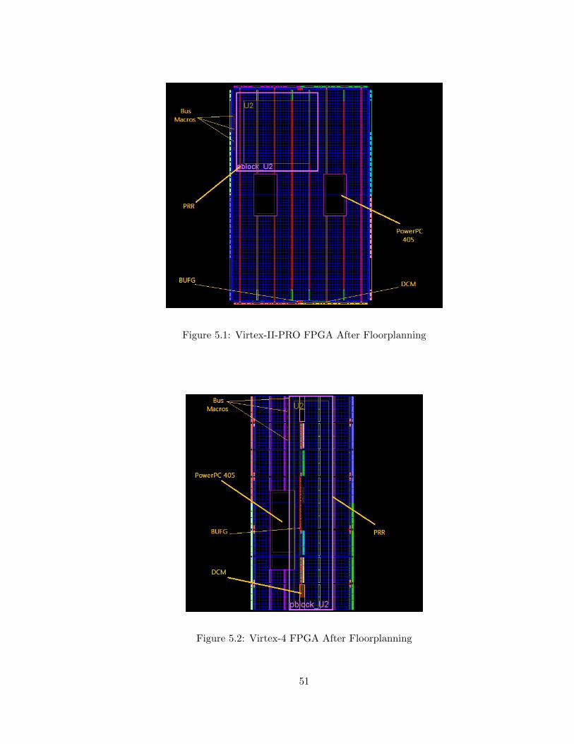
Figure 5.1: Virtex-II-PRO FPGA After Floorplanning
Figure 5.2: Virtex-4 FPGA After Floorplanning
51
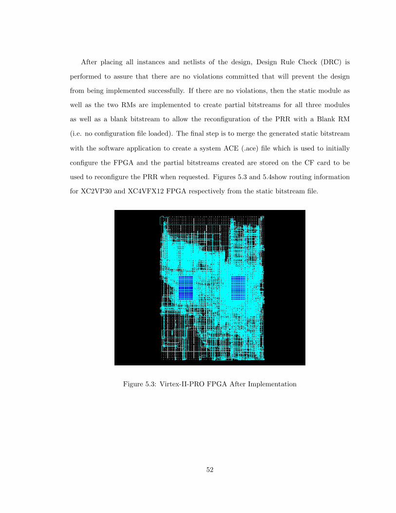
After placing all instances and netlists of the design, Design Rule Check (DRC) is
performed to assure that there are no violations committed that will prevent the design
from being implemented successfully. If there are no violations, then the static module as
well as the two RMs are implemented to create partial bitstreams for all three modules
as well as a blank bitstream to allow the reconfiguration of the PRR with a Blank RM
(i.e. no configuration file loaded). The final step is to merge the generated static bitstream
with the software application to create a system ACE (.ace) file which is used to initially
configure the FPGA and the partial bitstreams created are stored on the CF card to be
used to reconfigure the PRR when requested. Figures 5.3 and 5.4show routing information
for XC2VP30 and XC4VFX12 FPGA respectively from the static bitstream file.
Figure 5.3: Virtex-II-PRO FPGA After Implementation
52

Figure 5.4: Virtex-4 FPGA After Implementation
5.6 Problems
Although the previous steps mentioned to perform partial reconfiguration seems straight
forward, we encountered a number of problems through different design and implementation
phases that we had to solve for the system to perform as expected. In this section we will
discuss some of these problems and the solution we found
• During the static portion designing phase in EDK, there was a problem regarding the
communication between hardware and software which we solved using the synchro-
nization circuit that prevented the hardware from receiving input or sending output
before the software is ready to send and receive respectively.
• The custom peripheral we created to instantiate the AES and SHA-256 cores to the
system was initially interfaced to the OPB bus using IPIF with the support of FIFO to
allow data to be sent and received faster between the software and the hardware. The
53
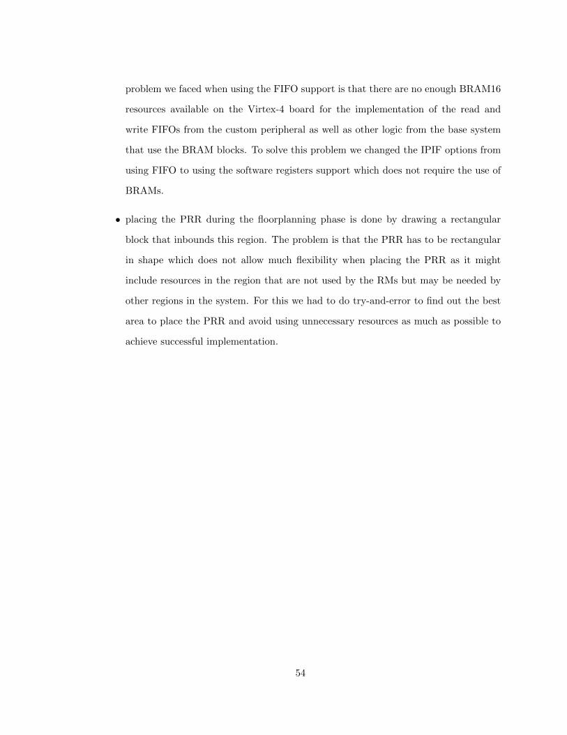
problem we faced when using the FIFO support is that there are no enough BRAM16
resources available on the Virtex-4 board for the implementation of the read and
write FIFOs from the custom peripheral as well as other logic from the base system
that use the BRAM blocks. To solve this problem we changed the IPIF options from
using FIFO to using the software registers support which does not require the use of
BRAMs.
• placing the PRR during the floorplanning phase is done by drawing a rectangular
block that inbounds this region. The problem is that the PRR has to be rectangular
in shape which does not allow much flexibility when placing the PRR as it might
include resources in the region that are not used by the RMs but may be needed by
other regions in the system. For this we had to do try-and-error to find out the best
area to place the PRR and avoid using unnecessary resources as much as possible to
achieve successful implementation.
54

Chapter 6: Results
6.1 Device Utilization Summary
We implemented two different versions of the PR embedded system using PowerPC and
Microblaze on two different platforms, The ML403 and XUP Virtex-II-Pro boards as well
as implementations for the AES and SHA-256 cores as non-PR designs within an embedded
system and as independent cores to compare them to the PR designs in terms of area and
resources used. Table 6.1 represents the results for different implementations on the ML403.
the first two columns summarize the resources of the static and dynamic portions of the
system. columns three and four are implementation results for each of the two cores (AES
and SHA-256) implemented in an embedded system separately and the last two columns
are results for implementing each core independently in non-PR designs.
Table 6.1: Resources Summary for Implementations on ML403 Board
Device Utilization PR Design Non-PR Non-PR
Summary PR Design Embedded System Implementation
Resource Logic Static Dynamic AES SHA-256 AES core SHA-256 core
Number of Slices 1588 2148 4066 2200 1862 924
Number of Slice Flip Flops 1566 1008 2525 2198 807 1008
Number of 4 input LUTs 2059 3600 6951 3118 3600 1620
Number of bonded IOBs 32 0 100 95 320 320
Number of FIFO16/RAMB16s 33 0 34 33 1 0
Number of GCLKs 2 0 2 2 0 0
Number of PPC405s 1 0 1 1 0 0
Number of DCMs 1 0 1 1 0 0
55

It can be shown from the results that implementing both cores in a PR design (3736
slices) not only saves more than 40% of the design area compared to the non-PR embedded
design with both cores (6266 slices) but it also makes the implementation of both these cores
within the same embedded system feasible for this platform as the Virtex-4 device on the
ML403 does not have enough resources to implement a non-PR embedded system with both
cores. Also when comparing the static portion in the design to the non-PR implementations,
it can be noticed that the PR design uses 2148 slices compared to 2786 slices used by the
two non-PR designs combined together with more than 25% area improvement and these
area savings are open to further improvement if more reconfigurable modules are added to
the same reconfigurable region.
Table 6.2 shows the results from implementations on the XUP Virtex-II-Pro board using
PowerPC as the embedded processor. We implemented the same designs described above
on the Virtex-II-Pro device. The PR-design uses 3736 slices for both static and dynamic
regions while the non-PR implementations of both cores use 6266 slices showing over 40%
improvement in area optimization similar to results obtained from ML403 implementations.
In addition to implementations similar to those we performed on the ML403 board, we
also implemented the PR and non-PR embedded system designs using Microblaze as the
embedded processor in the system on the Virtex-II-Pro platform.
56

Table 6.2: Resources Summary for PowerPC Implementations on Virtex-II-Pro
Device Utilization PR Design Non-PR Non-PR
Summary PowerPC System PowerPC System Implementation
Resource Logic Static Dynamic AES SHA-256 AES core SHA-256 core
Number of Slices 1610 2150 4589 2683 1863 853
Number of Slice Flip Flops 1608 1006 2514 2597 807 976
Number of 4 input LUTs 2024 3621 6951 3511 3602 1444
Number of bonded IOBs 32 0 32 32 556 556
Number of BRAMs 49 1 49 50 0 1
Number of GCLKs 2 0 2 2 0 0
Number of ICAPs 1 0 0 0 0 0
Number of PPC405s 1 0 1 1 0 0
Number of DCMs 1 0 1 1 0 0
The results shown in Table 6.3 are for the Microblaze implementations on the Virtex-II-
Pro platform. The area overhead is caused by resources used by the Microblaze processor
itself as it requires additional resources during synthesis and implementation unlike the
hard core PowerPC which does not require as much resources but the overall area improve-
ments from the non-PR design to the PR one are similar to those obtained from PowerPC
implementations.
57

Table 6.3: Resources Summary for Microblaze Implementations on Virtex-II-Pro
Device Utilization PR Design Non-PR Non-PR
Summary Microblaze System Microblaze System Implementation
Resource Logic Static Dynamic AES SHA-256 AES core SHA-256 core
Number of Slices 2114 2148 3693 2763 1863 853
Number of Slice Flip Flops 2108 1063 2648 2849 807 976
Number of 4 input LUTs 2557 4194 6154 4164 3602 1444
Number of bonded IOBs 30 0 32 32 556 556
Number of BRAMs 52 1 52 53 0 1
Number of ICAPs 1 0 0 0 0 0
Number of GCLKs 2 0 2 2 0 0
Number of DCMs 1 0 1 1 0 0
6.2 Time Measurements
In addition to area and resources results, we wanted to perform time measurements for the
amount of time needed to perform partial reconfiguration between the two hardware mod-
ules. Time measurements in [40] are performed by obtaining the amount of time needed
to reconfigure the whole FPGA from the device data-sheet and calculating reconfiguration
time per frame then they estimate amount of time needed to perform partial reconfigu-
ration for the number of frames in the partial bitstream. in [41] they perform real-time
measurements but the method is not explained.
To calculate the partial reconfiguration time, we used xtime library provided by Xilinx
software libraries. it provide access to the 64-bit time base counter inside the PowerPC core
which increases by one at every processor cycle [42]. The XTime GetTime() function writes
the current value of the time base register to a specified variable, we call this function before
partial reconfiguration and we recall it again after the process is done and the difference
between both obtained values is the reconfiguration time. We consider the reconfiguration
58

process to start from the time the bus macros are being disabled until they are enabled
again thus taking the enabling/disabling time into consideration when calculating for time
as shown in Figure 6.1.
BMEnableBM
ICAP Reconfiguration Disable
Figure 6.1: Total Time Needed for Partial Reconfiguration
Time measurements were performed using the same method described in [43] on the PR
embedded designs with PowerPC processor running at 100 Mhz on both platforms. Table
6.4 shows the results obtained from both platforms for a given design. The first column
represents the platform on which the design was tested and whether the PowerPC cache
was enabled or disabled. The second (Design 1) is for the size and reconfiguration speed for
the reconfigurable design we are researching and the third column (Design 2) is for a smaller
design which we use to show the difference in speed for small and large designs. The fourth
59
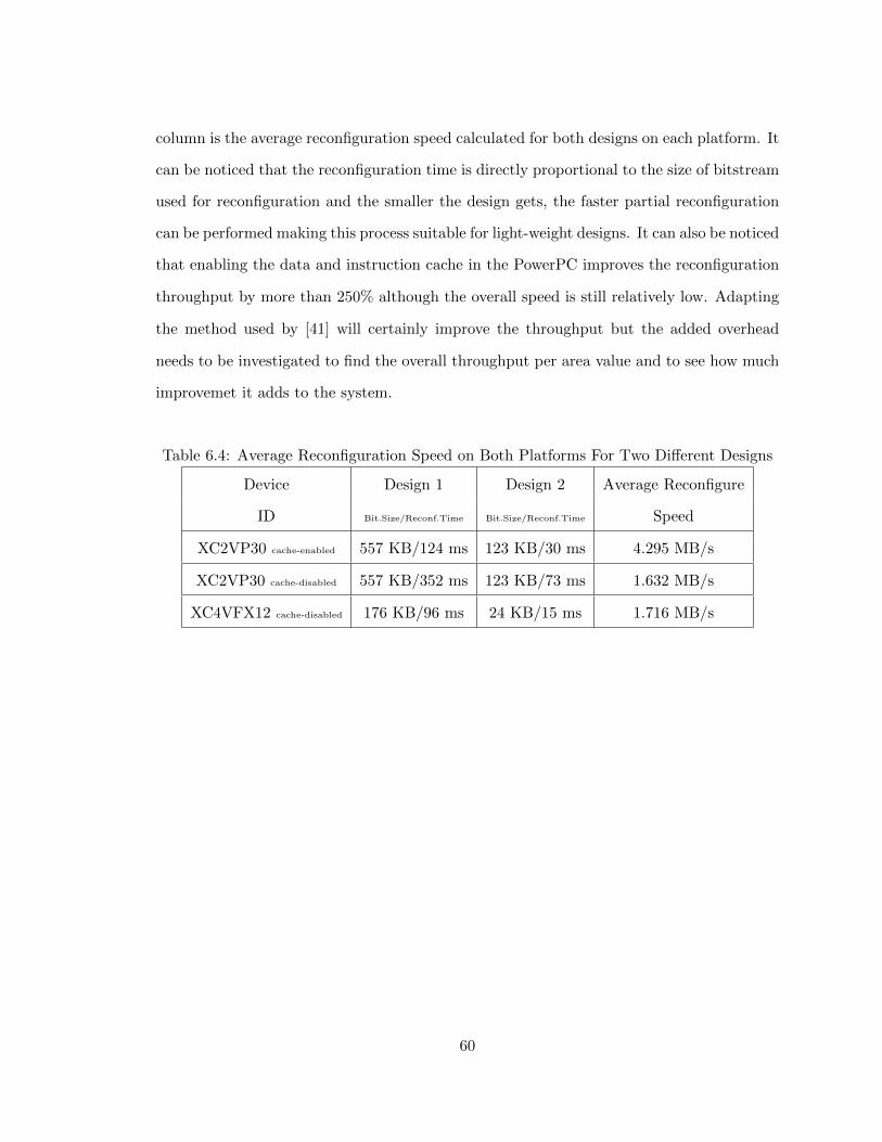
column is the average reconfiguration speed calculated for both designs on each platform. It
can be noticed that the reconfiguration time is directly proportional to the size of bitstream
used for reconfiguration and the smaller the design gets, the faster partial reconfiguration
can be performed making this process suitable for light-weight designs. It can also be noticed
that enabling the data and instruction cache in the PowerPC improves the reconfiguration
throughput by more than 250% although the overall speed is still relatively low. Adapting
the method used by [41] will certainly improve the throughput but the added overhead
needs to be investigated to find the overall throughput per area value and to see how much
improvemet it adds to the system.
Table 6.4: Average Reconfiguration Speed on Both Platforms For Two Different Designs
Device Design 1 Design 2 Average Reconfigure
ID Bit.Size/Reconf.Time Bit.Size/Reconf.Time Speed
XC2VP30 cache-enabled 557 KB/124 ms 123 KB/30 ms 4.295 MB/s
XC2VP30 cache-disabled 557 KB/352 ms 123 KB/73 ms 1.632 MB/s
XC4VFX12 cache-disabled 176 KB/96 ms 24 KB/15 ms 1.716 MB/s
60

Chapter 7: Conclusion
In this thesis, we successfully designed and implemented IPsec protocol on FPGA using
partial reconfiguration allowing the use of less resources. Authentication and confidential-
ity services in IPsec are provided through SHA-256 and AES hardware accelerator cores
implemented as reconfigurable modules in the system.
The implementation process included creating embedded systems with PowerPC and
Microblaze embedded processors as the static portion of the design to allow the system to
be self-reconfigurable. The embedded system is composed of the processor, the OPB,PLB
and DCR buses and the HWICAP, system ACE, UART peripherals. The dynamic portion
in the system or the reconfigurable region is composed of the AES and SHA-256 modules as
reconfigurable modules. Through ICAP, the processor reconfigures the reconfigurable region
with one of the two reconfigurable modules depending on the security service requested
by the application being processed by the software. A synchronization circuit was also
implemented between the hardware and software to provide smooth communication. The
static and dynamic modules were synthesized and floorplanned separately then merged
together in the final PR-assemble phase of the implementation process.
All designs were implemented and tested for functionality on two different Xilinx boards,
ML403 and Virtex-II-Pro, to assure that the design is suitable for different platforms. Re-
sults shows significant improvements in terms of area between the PR and non-PR designs
which can be further improved if more reconfigurable modules are assigned to the same
reconfigurable region. Time measurements for partial reconfiguration shows that reconfig-
uration speed is directly proportional to the partial bitstream size making this technique
more suitable for smaller designs like light-weight implementations.
61
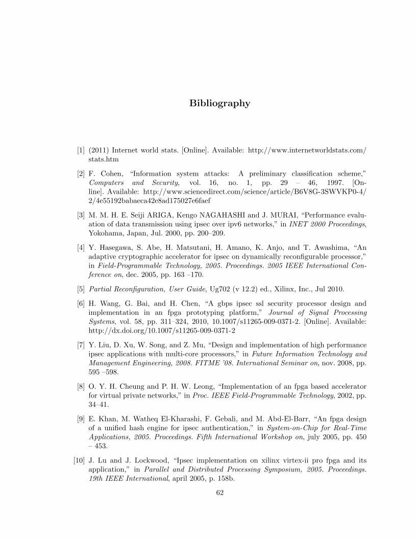
Bibliography
[1] (2011) Internet world stats. [Online]. Available: http://www.internetworldstats.com/stats.htm
[2] F. Cohen, “Information system attacks: A preliminary classification scheme,”Computers and Security, vol. 16, no. 1, pp. 29 – 46, 1997. [On-line]. Available: http://www.sciencedirect.com/science/article/B6V8G-3SWVKP0-4/2/4e55192babaeca42e8ad175027e6faef
[3] M. M. H. E. Seiji ARIGA, Kengo NAGAHASHI and J. MURAI, “Performance evalu-ation of data transmission using ipsec over ipv6 networks,” in INET 2000 Proceedings,Yokohama, Japan, Jul. 2000, pp. 200–209.
[4] Y. Hasegawa, S. Abe, H. Matsutani, H. Amano, K. Anjo, and T. Awashima, “Anadaptive cryptographic accelerator for ipsec on dynamically reconfigurable processor,”in Field-Programmable Technology, 2005. Proceedings. 2005 IEEE International Con-ference on, dec. 2005, pp. 163 –170.
[5] Partial Reconfiguration, User Guide, Ug702 (v 12.2) ed., Xilinx, Inc., Jul 2010.
[6] H. Wang, G. Bai, and H. Chen, “A gbps ipsec ssl security processor design andimplementation in an fpga prototyping platform,” Journal of Signal ProcessingSystems, vol. 58, pp. 311–324, 2010, 10.1007/s11265-009-0371-2. [Online]. Available:http://dx.doi.org/10.1007/s11265-009-0371-2
[7] Y. Liu, D. Xu, W. Song, and Z. Mu, “Design and implementation of high performanceipsec applications with multi-core processors,” in Future Information Technology andManagement Engineering, 2008. FITME ’08. International Seminar on, nov. 2008, pp.595 –598.
[8] O. Y. H. Cheung and P. H. W. Leong, “Implementation of an fpga based acceleratorfor virtual private networks,” in Proc. IEEE Field-Programmable Technology, 2002, pp.34–41.
[9] E. Khan, M. Watheq El-Kharashi, F. Gebali, and M. Abd-El-Barr, “An fpga designof a unified hash engine for ipsec authentication,” in System-on-Chip for Real-TimeApplications, 2005. Proceedings. Fifth International Workshop on, july 2005, pp. 450– 453.
[10] J. Lu and J. Lockwood, “Ipsec implementation on xilinx virtex-ii pro fpga and itsapplication,” in Parallel and Distributed Processing Symposium, 2005. Proceedings.19th IEEE International, april 2005, p. 158b.
62
[11] A. Dandalis, V. Prasanna, and J. Rolim, “An adaptive cryptographic engine for ipsecarchitectures,” in Field-Programmable Custom Computing Machines, 2000 IEEE Sym-posium on, 2000, pp. 132 –141.
[12] C.-C. Cheng, W.-M. Chen, H.-C. Chao, and Y.-P. Wang, “Fpga authentication header(ah) implementation for internet appliances,” in Dependable Computing, 2005. Pro-ceedings. 11th Pacific Rim International Symposium on, dec. 2005, p. 6 pp.
[13] D. Zibin and Z. Ning, “Fpga implementation of sha-1 algorithm,” in ASIC, 2003.Proceedings. 5th International Conference on, vol. 2, oct. 2003, pp. 1321 – 1324 Vol.2.
[14] A. H. S. Zeineddini, “Secure partial reconfiguration of fpgas,” Master’s thesis, GeorgeMason University, Fairfax,VA, 2005.
[15] W. Stallings, Cryptography and Network Security: Principles and Practice. PrenticeHall, 2010.
[16] P. v. O. A. Menezes and S. Vanstone, Handbook of Applied Cryptography. CRC Press,1996.
[17] S. Kent, “Ip authentication header,” RFC 4302, Dec 2005.
[18] ——, “Ip encapsulating security payload (esp),” RFC 4303, Dec 2005.
[19] The free S WAN Website, FREESWAN, Org.,http://www.freeswan.org/freeswansnaps/CURRENT −SNAP/doc/ipsec.html, Jan2004.
[20] Virtex 2.5 V Field Programmable Gate Arrays, Product Specification, Ds003-1 (v2.5 ) ed.,Xilinx, Inc., Apr 2001.
[21] Virtex-II Pro and Virtex-II Pro X Platform FPGAs: Complete Data Sheet, Product Speci-fication, Ds083 (v4.7) ed., Xilinx, Inc., Nov 2007.
[22] Xilinx University Program Virtex-II Pro Development System, Hardware Reference Manual,Ug069 (v1.2) ed., Xilinx, Inc., Jul 2009.
[23] Virtex-4 Family Overview, Product Specification, Ds112 (v3.1) ed., Xilinx, Inc., Aug 2010.
[24] ML401/ML402/ML403 Evaluation Platform, User Guide, Ug080 (v2.5) ed., Xilinx, Inc.,May 2006.
[25] Virtex-4 FPGA, User Guide, Ug070 (v2.6) ed., Xilinx, Inc., Dec 2008.
[26] Embedded System Tools Reference Manual, User Guide, Ug111 (v7.0) ed., Xilinx, Inc., Jan2007.
[27] PlanAhead, User Guide, Ug632 (v 11.4) ed., Xilinx, Inc., Dec 2009.
[28] B. Jackson, Partial Reconfiguration Design with PlanAhead, User Guide, (v 2.1) ed., Xilinx,Inc., Mar 2008.
63

[29] Two Flows for Partial Reconfiguration: Module Based or Difference Based, ApplicationNote, Xapp290 (v1.2) ed., Xilinx, Inc., Sep 2004.
[30] Early Access Partial Reconfiguration, User Guide, Ug208 (v1.1) ed., Xilinx, Inc., Mar 2006.
[31] Virtex-4 FX12 PowerPC and MicroBlaze Edition Kit Reference Systems, User Guide,Ug494 (v1.1) ed., Xilinx, Inc., May 2008.
[32] CoreConnect Bus Architecture, User Guide, Gk10 ed., IBM, Inc., May 1999.
[33] Processor Local Bus (PLB) v3.4 (v1.02a), Product Specification, Ds400 ed., Xilinx, Inc.,Apr 2009.
[34] On-Chip Peripheral Bus V2.0 with OPB Arbiter (v1.10c) , Product Specification, Ds401 ed.,Xilinx, Inc., Aug 2006.
[35] LogiCORE IP Device Control Register Bus (DCR) v2.9 (v1.00b), Product Specification,Ds402 ed., Xilinx, Inc., Apr 2009.
[36] “Specification for the advanced encryption standard (aes),” Federal Information ProcessingStandards Publication 197, 2001. [Online]. Available: http://csrc.nist.gov/publications/fips/fips197/fips-197.pdf
[37] F. I. Processing, P. J. Bond, U. Secretary, A. L. Bement, and W. M. Director, “Fips pub198,” Tech. Rep., 1990.
[38] B. Blodget, P. James-Roxby, E. Keller, S. McMillan, and P. Sundararajan, “A self-reconfiguring platform,” in Field Programmable Logic and Application, ser. Lecture Notesin Computer Science, P. Y. K. Cheung and G. Constantinides, Eds., vol. 2778. SpringerBerlin / Heidelberg, 2003, pp. 565–574.
[39] Xilinx Device Drivers Documentation, Product Specification, 1st ed., Xilinx, Inc., Jun 2004.
[40] K. Paulsson, M. Hubner, and J. Becker, “Exploitation of dynamic and partial hardwarereconfiguration for on-line power/performance optimization,” in Field Programmable Logicand Applications, 2008. FPL 2008. International Conference on, sept. 2008, pp. 699 –700.
[41] M. Liu, W. Kuehn, Z. Lu, and A. Jantsch, “Run-time partial reconfiguration speed in-vestigation and architectural design space exploration,” in Field Programmable Logic andApplications, 2009. FPL 2009. International Conference on, 31 2009-sept. 2 2009, pp. 498–502.
[42] Standalone Board Support Package, Product Specification, 9th ed., Xilinx, Inc., Jan 2007.
[43] C. Claus, F. Muller, J. Zeppenfeld, and W. Stechele, “A new framework to acceleratevirtex-ii pro dynamic partial self-reconfiguration,” in Parallel and Distributed ProcessingSymposium, 2007. IPDPS 2007. IEEE International, march 2007, pp. 1 –7.
64

Curriculum Vitae
Ahmad Salman was born on August 30th, 1980 in Alexandria, Egypt. He received herBachelor of Engineering Degree from Arab Academy For Scince and Technology School ofEngineering, Alexandria, Egypt in May 2002. He started working towards his Master ofScience degree in Computer Engineering from August 2007 at George Mason University.As a Teaching Assistant, he handled various undergraduate courses and a graduate courseat George Mason University. A research student with Cryptographic Engineering ResearchGroup (CERG), his focus was on performing dynamic partial reconfiguration on FPGAplatforms. He worked as an instructor at Duke University summers 2008,2009 and 2010,designing and teaching a cryptography course allowing him to expand his knowledge on thetopic and improve his teaching skills.
65