Embed Size (px)
Citation preview
IP CORE DESIGN OF MICROCONTROLLER SYSTEM USING VERILOG
FOR ROBOT BASED AGRICULTURAL IMPLEMENTS
C. S. Mala*, S. Ramachandran#
* Jawaharlal Nehru Technological University, Hyderabad, # SJB Institute of Technology, Bangalore
[email protected], [email protected]
ABSTRACT
This paper presents an RTL compliant Verilog IP
Core design of a Microcontroller System modeled
on the popular 8051 of Intel. This requirement
primarily stems from the on-going project to design
a Robot based Agricultural Implement. The
proposed system consists of a core processor which
emulates the existing 8051 Microcontroller. The
designed core has 4K internal ROM, 128 bytes of
internal RAM, address generator, decoder, external
64 KB RAM and external 60 KB ROM. The
external RAM and ROM is user configurable. The
IP Core realizes most of the 8051 features except
that connected with serial communication. They
have been fully tested using a comprehensive Test
bench, also coded using Verilog. The RTL design is
platform and technology independent. The
Agricultural Implement design has been targeted on
the Xilinx FPGA, Spartan 3, 200. The designed
system is more efficient in terms of processing
speed by over 8 to 50 times when compared to the
original Intel‟s 8051.
KEYWORDS
IP Core, Verilog, Register Transfer Logic, Robot,
Agricultural Implement.
1. INTRODUCTION
Embedded systems are compact, sophisticated
and application specific systems used in real
time applications. Embedded systems are
widely built with microcontrollers as
standalone systems. Microcontrollers contain
on chip input and output ports, memories,
timers etc. , and they can be used for any
specific application needing small to medium
throughputs.
In order to speed up processing of 8051
instructions on an FPGA or an ASIC, an
Intellectual Property (IP) Core for 8051 based
system has been designed using Verilog in the
present work. An IP Core is a predefined,
verified and tested code block and can be used
as a Plug and Play device in a system. IP Cores
are reconfigurable and reusable systems. The IP
Core developed can be used for all applications,
whether they are for a past product, the current
ongoing project or for future applications. It
may be noted that even obsolete
Microcontrollers or Microprocessors can be
given a new lease of life by developing their IP
Cores. Since 8051 microcontroller has outlived
its age already, we have designed its IP Core in
order to insure it against its obsolescence.
Yuanyuan et al. [1] have developed a Single-
Chip Speech Recognition System based on
8051 MicrocontroIler. However, this work
does not realize the 8051 core. The authors
have claimed ten times lower cost than a DSP
core. A. Moore, Scott [2] and Aviral Mittal [3]
have developed IP Cores for 8080 CPU (using
Verilog) and 8085 (using VHDL) respectively.
They are RTL compliant. R. V. Siva Reddy, S.
Ramachandran and K. Nagabhushana Raju [4]
have developed IP Core for 8085 in Verilog
conforming to RTL guidelines and have used
the core for Electrostatic Precipitator processor
213
which has achieved significant speed of
operation (over 30 folds) compared to 8085
based systems used presently in the thermal
power plants. In order that a design may work
on a chip without any hassles, RTL
conformance is mandatory [5].
N. Noguchi et al. [6] have automated
agricultural system for field applications. The
authors have developed a robot for agricultural
operation. They have used navigation sensor, an
RTK-GPS and an inertial measurement unit
(IMU) for navigation through the field.
However, this implementation is tractor
mounted and is expensive.
K. C. Jones [7] has implemented robots to weed
out farms which make their way through a field
with precision weed-destroyers onboard. The
Robot itself weighs about 450-650 pounds and
does not completely do away with human labor.
D. W. I. Brooke [8] claims to have improved
the performance of existing tractor mounted
agricultural system. His stress was more
towards automating for improved energy
management including waste recycling.
Zhang. X et al. [9] have developed an electronic
controlled platooning system, which will enable
an autonomous agricultural vehicle to follow a
leading tractor with a given lateral and
longitudinal offset. He has employed RTK GPS
system and wireless Modems for positioning
and tracking of the Tractor.
Chen Jun et al. [10] described an agricultural
mobile robot which was refitted by FT4040
tractor. The tracking control was researched
using fuzzy logic. The stress was more on
designing a fuzzy controller for straight-line
tracking.
In Eaton. R. et al. work [11], the autonomous
farm is seen as a complex system, which deals
with issues of agronomy. The agricultural
robotics uses on-farm sensing and control to
actuate autonomous farm machinery with the
aim of satisfying agronomy-based objectives.
The preliminary results highlight the
autonomous control of vehicles for the
operations of crop seeding and non-herbicidal
weeding.
The present work aims at developing a
Microcontroller system for Robot Based
Agricultural Implement such as a Plough that
would automate ploughing operations and
reduce considerable amount of labor and time.
With the intent of improving the throughput
and reducing the system cost, we propose here
the design of an Intellectual Property (IP) Core
for our system so that it may be implemented
on an FPGA or as an ASIC.
The paper is organized as follows. Section 2
presents the basic Architecture of a Robotic
system for automating ploughing operations.
Section 3 presents the design of IP Core of the
Micro Controller System. Section 4 presents
the development of Algorithmic State Machine
(ASM) charts, a design aid for processing
instructions in an efficient manner. Various
groups of instructions are implemented in this
work and the processing speed achieved is
compared with that of the Intel‟s 8051
Microcontroller [12-14]. The simulation results
are presented in Section 5. The last section
presents the conclusions derived as well as
work for future enhancements.
2. BASIC ARCHITECTURE OF THE
PROPOSED ROBOT BASED
AGRICULTURAL IMPLEMENT
SYSTEM
This work proposes the development of IP Core
for automating agricultural implements from
tilling to other agricultural practices, which is
currently animal drawn or tractor mounted. A
driverless Robotic vehicle system is being
designed in order to speed up agricultural work
and reap richer harvests. The length and breadth
of the field along with the spacing between the
till lines are made user programmable. To
commence tilling of a land, the Robotic vehicle
along with the plough is positioned as shown on
the top left of Fig. 1. The farmer with little
training specifies the length, breadth and
214
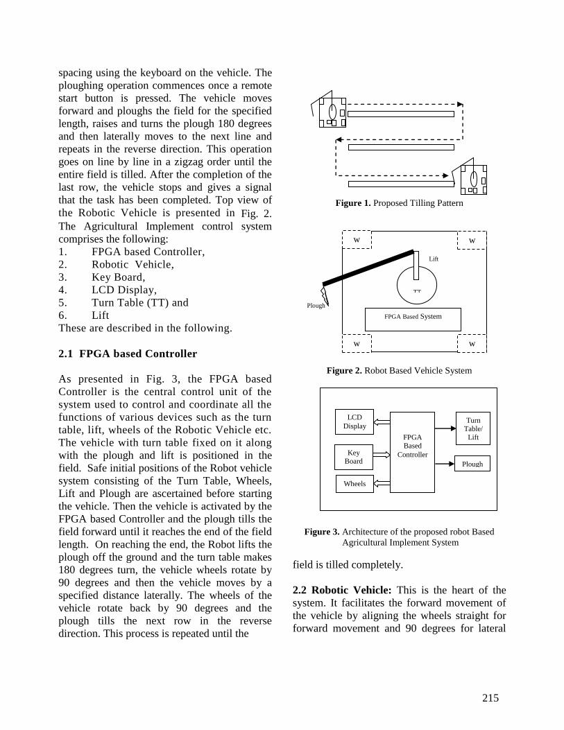
spacing using the keyboard on the vehicle. The
ploughing operation commences once a remote
start button is pressed. The vehicle moves
forward and ploughs the field for the specified
length, raises and turns the plough 180 degrees
and then laterally moves to the next line and
repeats in the reverse direction. This operation
goes on line by line in a zigzag order until the
entire field is tilled. After the completion of the
last row, the vehicle stops and gives a signal
that the task has been completed. Top view of
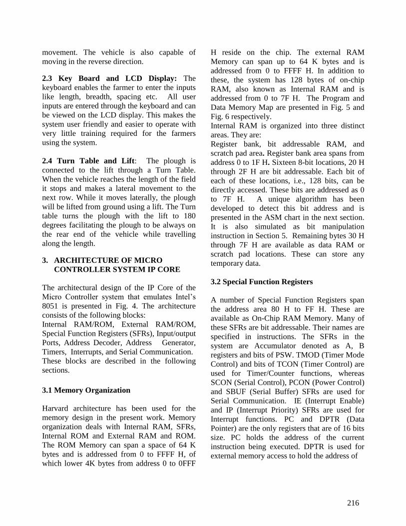
the Robotic Vehicle is presented in Fig. 2.
The Agricultural Implement control system
comprises the following:
1. FPGA based Controller,
2. Robotic Vehicle,
3. Key Board,
4. LCD Display,
5. Turn Table (TT) and
6. Lift
These are described in the following.
2.1 FPGA based Controller
As presented in Fig. 3, the FPGA based
Controller is the central control unit of the
system used to control and coordinate all the
functions of various devices such as the turn
table, lift, wheels of the Robotic Vehicle etc.
The vehicle with turn table fixed on it along with the plough and lift is positioned in the
field. Safe initial positions of the Robot vehicle
system consisting of the Turn Table, Wheels,
Lift and Plough are ascertained before starting
the vehicle. Then the vehicle is activated by the
FPGA based Controller and the plough tills the
field forward until it reaches the end of the field
length. On reaching the end, the Robot lifts the
plough off the ground and the turn table makes
180 degrees turn, the vehicle wheels rotate by
90 degrees and then the vehicle moves by a
specified distance laterally. The wheels of the
vehicle rotate back by 90 degrees and the
plough tills the next row in the reverse
direction. This process is repeated until the
Figure 1. Proposed Tilling Pattern
Figure 2. Robot Based Vehicle System
Figure 3. Architecture of the proposed robot Based
Agricultural Implement System
field is tilled completely.
2.2 Robotic Vehicle: This is the heart of the
system. It facilitates the forward movement of
the vehicle by aligning the wheels straight for
forward movement and 90 degrees for lateral
Plough
w
WW
FPGA Based System
TT
Lift
w
WW
w
WW
w
WW
LCD
Display
Key Board
Display
Wheels
FPGA
Based
Controller
Turn Table/
Lift
Plough
215
movement. The vehicle is also capable of
moving in the reverse direction.
2.3 Key Board and LCD Display: The
keyboard enables the farmer to enter the inputs
like length, breadth, spacing etc. All user
inputs are entered through the keyboard and can
be viewed on the LCD display. This makes the
system user friendly and easier to operate with
very little training required for the farmers
using the system.
2.4 Turn Table and Lift: The plough is
connected to the lift through a Turn Table.
When the vehicle reaches the length of the field
it stops and makes a lateral movement to the
next row. While it moves laterally, the plough
will be lifted from ground using a lift. The Turn
table turns the plough with the lift to 180
degrees facilitating the plough to be always on
the rear end of the vehicle while travelling
along the length.
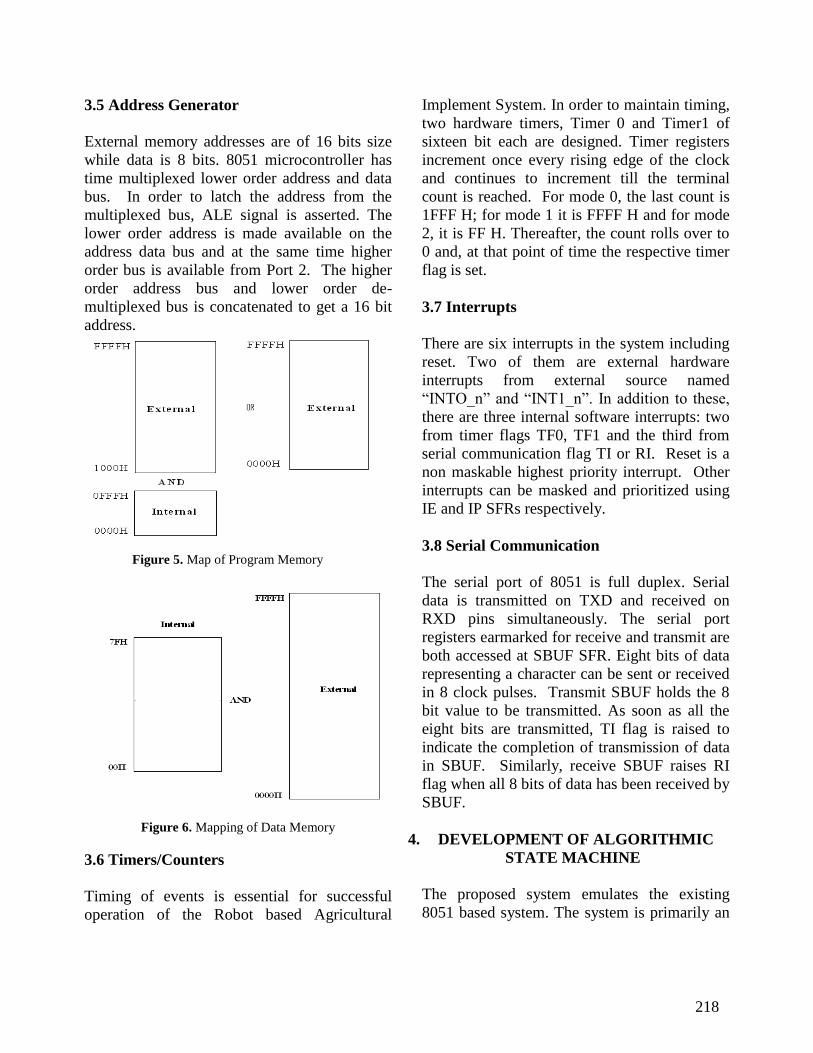
3. ARCHITECTURE OF MICRO
CONTROLLER SYSTEM IP CORE
The architectural design of the IP Core of the
Micro Controller system that emulates Intel‟s
8051 is presented in Fig. 4. The architecture
consists of the following blocks:
Internal RAM/ROM, External RAM/ROM,
Special Function Registers (SFRs), Input/output
Ports, Address Decoder, Address Generator,
Timers, Interrupts, and Serial Communication.
These blocks are described in the following
sections.
3.1 Memory Organization
Harvard architecture has been used for the
memory design in the present work. Memory
organization deals with Internal RAM, SFRs,
Internal ROM and External RAM and ROM.
The ROM Memory can span a space of 64 K
bytes and is addressed from 0 to FFFF H, of
which lower 4K bytes from address 0 to 0FFF
H reside on the chip. The external RAM
Memory can span up to 64 K bytes and is
addressed from 0 to FFFF H. In addition to
these, the system has 128 bytes of on-chip
RAM, also known as Internal RAM and is
addressed from 0 to 7F H. The Program and
Data Memory Map are presented in Fig. 5 and
Fig. 6 respectively.
Internal RAM is organized into three distinct
areas. They are:
Register bank, bit addressable RAM, and
scratch pad area. Register bank area spans from
address 0 to 1F H. Sixteen 8-bit locations, 20 H
through 2F H are bit addressable. Each bit of
each of these locations, i.e., 128 bits, can be
directly accessed. These bits are addressed as 0
to 7F H. A unique algorithm has been
developed to detect this bit address and is
presented in the ASM chart in the next section.
It is also simulated as bit manipulation
instruction in Section 5. Remaining bytes 30 H
through 7F H are available as data RAM or
scratch pad locations. These can store any
temporary data.
3.2 Special Function Registers
A number of Special Function Registers span
the address area 80 H to FF H. These are
available as On-Chip RAM Memory. Many of
these SFRs are bit addressable. Their names are
specified in instructions. The SFRs in the
system are Accumulator denoted as A, B
registers and bits of PSW. TMOD (Timer Mode
Control) and bits of TCON (Timer Control) are
used for Timer/Counter functions, whereas
SCON (Serial Control), PCON (Power Control)
and SBUF (Serial Buffer) SFRs are used for
Serial Communication. IE (Interrupt Enable)
and IP (Interrupt Priority) SFRs are used for
Interrupt functions. PC and DPTR (Data
Pointer) are the only registers that are of 16 bits
size. PC holds the address of the current
instruction being executed. DPTR is used for
external memory access to hold the address of
216
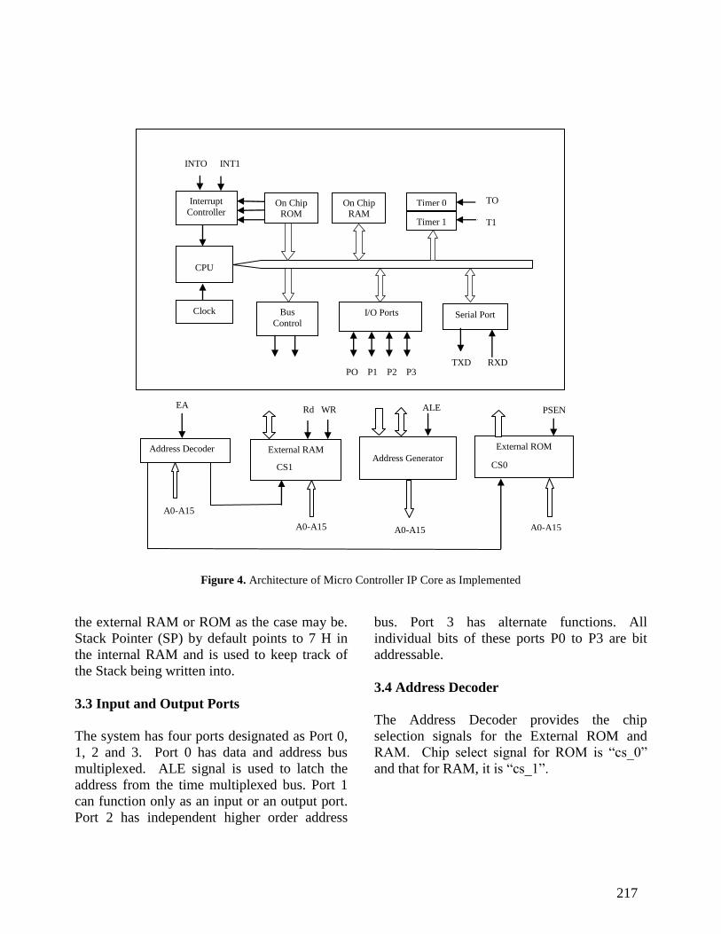
Figure 4. Architecture of Micro Controller IP Core as Implemented
the external RAM or ROM as the case may be.
Stack Pointer (SP) by default points to 7 H in
the internal RAM and is used to keep track of
the Stack being written into.
3.3 Input and Output Ports
The system has four ports designated as Port 0,
1, 2 and 3. Port 0 has data and address bus
multiplexed. ALE signal is used to latch the
address from the time multiplexed bus. Port 1
can function only as an input or an output port.
Port 2 has independent higher order address
bus. Port 3 has alternate functions. All
individual bits of these ports P0 to P3 are bit
addressable.
3.4 Address Decoder
The Address Decoder provides the chip
selection signals for the External ROM and
RAM. Chip select signal for ROM is “cs_0”
and that for RAM, it is “cs_1”.
Bus
Control
INTO INT1
CPU
Clock
On Chip ROM
On Chip RAM
Timer 0
Timer 1
I/O Ports Serial Port
Interrupt
Controller
PO P1 P2 P3 TXD RXD
TO
T1
EA
Address Decoder
Rd WR
External RAM
CS1
ALE
Address Generator
External ROM
PSEN
A0-A15
CS0
A0-A15 A0-A15
A0-A15
217
3.5 Address Generator
External memory addresses are of 16 bits size
while data is 8 bits. 8051 microcontroller has
time multiplexed lower order address and data
bus. In order to latch the address from the
multiplexed bus, ALE signal is asserted. The
lower order address is made available on the
address data bus and at the same time higher
order bus is available from Port 2. The higher
order address bus and lower order de-
multiplexed bus is concatenated to get a 16 bit
address.
Figure 5. Map of Program Memory
Figure 6. Mapping of Data Memory
3.6 Timers/Counters
Timing of events is essential for successful
operation of the Robot based Agricultural
Implement System. In order to maintain timing,
two hardware timers, Timer 0 and Timer1 of
sixteen bit each are designed. Timer registers
increment once every rising edge of the clock
and continues to increment till the terminal
count is reached. For mode 0, the last count is
1FFF H; for mode 1 it is FFFF H and for mode
2, it is FF H. Thereafter, the count rolls over to
0 and, at that point of time the respective timer
flag is set.
3.7 Interrupts
There are six interrupts in the system including
reset. Two of them are external hardware
interrupts from external source named
“INTO_n” and “INT1_n”. In addition to these,
there are three internal software interrupts: two
from timer flags TF0, TF1 and the third from
serial communication flag TI or RI. Reset is a
non maskable highest priority interrupt. Other
interrupts can be masked and prioritized using
IE and IP SFRs respectively.
3.8 Serial Communication
The serial port of 8051 is full duplex. Serial
data is transmitted on TXD and received on
RXD pins simultaneously. The serial port
registers earmarked for receive and transmit are
both accessed at SBUF SFR. Eight bits of data
representing a character can be sent or received
in 8 clock pulses. Transmit SBUF holds the 8
bit value to be transmitted. As soon as all the
eight bits are transmitted, TI flag is raised to
indicate the completion of transmission of data
in SBUF. Similarly, receive SBUF raises RI
flag when all 8 bits of data has been received by
SBUF.
4. DEVELOPMENT OF ALGORITHMIC
STATE MACHINE
The proposed system emulates the existing
8051 based system. The system is primarily an
218
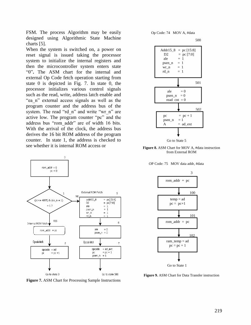
FSM. The process Algorithm may be easily
designed using Algorithmic State Machine
charts [5].
When the system is switched on, a power on
reset signal is issued taking the processor
system to initialize the internal registers and
then the microcontroller system enters state
“0”. The ASM chart for the internal and
external Op Code fetch operation starting from
state 0 is depicted in Fig. 7. In state 0, the
processor initializes various control signals
such as the read, write, address latch enable and
“ea_n” external access signals as well as the
program counter and the address bus of the
system. The read “rd_n” and write “wr_n” are
active low. The program counter “pc” and the
address bus “rom_addr” are of width 16 bits.
With the arrival of the clock, the address bus
derives the 16 bit ROM address of the program
counter. In state 1, the address is checked to
see whether it is internal ROM access or
Figure 7. ASM Chart for Processing Sample Instructions
Figure 8. ASM Chart for MOV A, #data instruction
from External ROM
Figure 9. ASM Chart for Data Transfer instruction
502
501
500
Go to State 5
Addr15_8 = pc [15:8]
D2 = pc [7:0]
ale = 1
psen_n = 1
wr_n = 1
rd_n = 1
ale = 0
psen_n = 0
read_cnt = 0
pc = pc + 1
psen_n = 1
A = ad_ext
Op Code: 74 MOV A, #data
3
rom_addr = pc
temp = ad
pc = pc+1
Go to State 1
rom_addr = pc
ram_temp = ad
pc = pc + 1
100
101
102
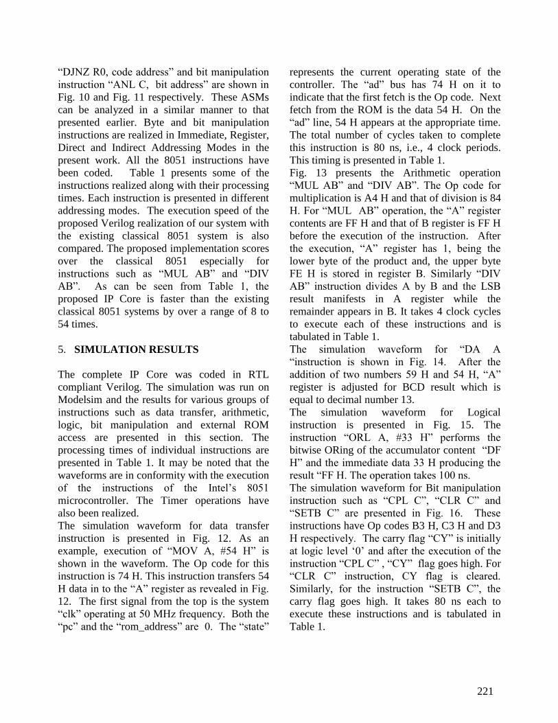
OP Code: 75 MOV data addr, #data
219
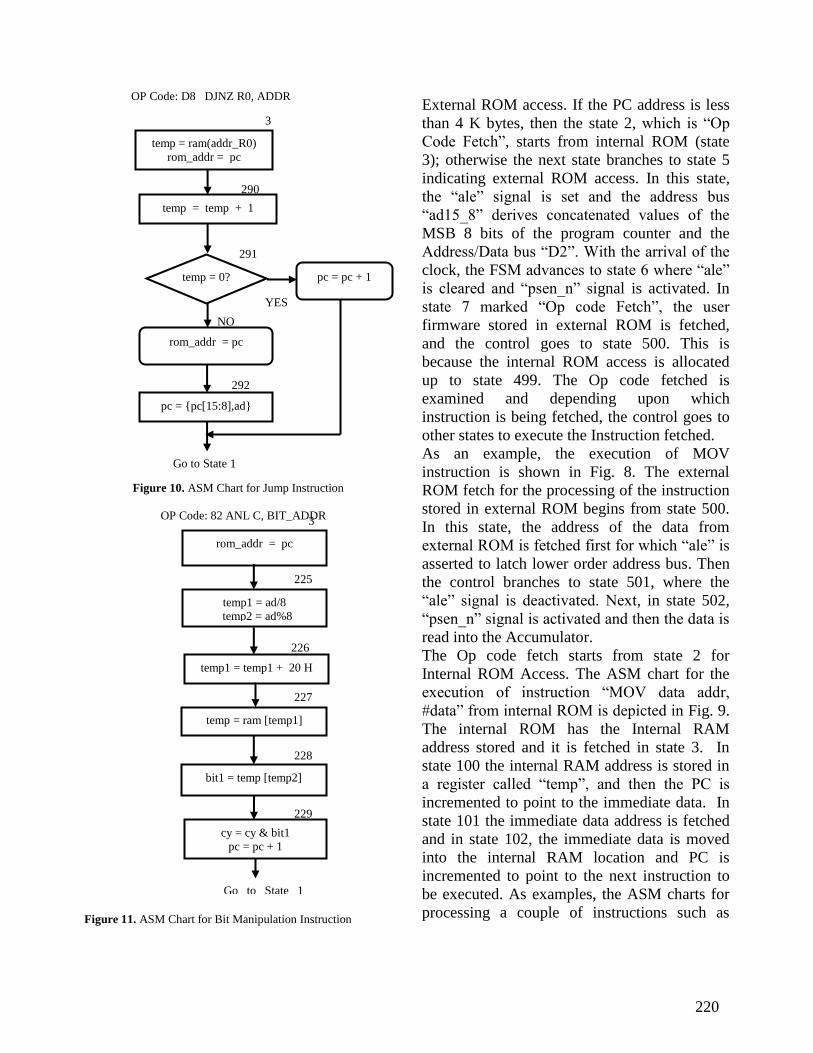
Figure 10. ASM Chart for Jump Instruction
Figure 11. ASM Chart for Bit Manipulation Instruction
External ROM access. If the PC address is less
than 4 K bytes, then the state 2, which is “Op
Code Fetch”, starts from internal ROM (state
3); otherwise the next state branches to state 5
indicating external ROM access. In this state,
the “ale” signal is set and the address bus
“ad15_8” derives concatenated values of the
MSB 8 bits of the program counter and the
Address/Data bus “D2”. With the arrival of the
clock, the FSM advances to state 6 where “ale”
is cleared and “psen_n” signal is activated. In
state 7 marked “Op code Fetch”, the user
firmware stored in external ROM is fetched,
and the control goes to state 500. This is
because the internal ROM access is allocated
up to state 499. The Op code fetched is
examined and depending upon which
instruction is being fetched, the control goes to
other states to execute the Instruction fetched.
As an example, the execution of MOV
instruction is shown in Fig. 8. The external
ROM fetch for the processing of the instruction
stored in external ROM begins from state 500.
In this state, the address of the data from
external ROM is fetched first for which “ale” is
asserted to latch lower order address bus. Then
the control branches to state 501, where the
“ale” signal is deactivated. Next, in state 502,
“psen_n” signal is activated and then the data is
read into the Accumulator.
The Op code fetch starts from state 2 for
Internal ROM Access. The ASM chart for the
execution of instruction “MOV data addr,
#data” from internal ROM is depicted in Fig. 9.
The internal ROM has the Internal RAM
address stored and it is fetched in state 3. In
state 100 the internal RAM address is stored in
a register called “temp”, and then the PC is
incremented to point to the immediate data. In
state 101 the immediate data address is fetched
and in state 102, the immediate data is moved
into the internal RAM location and PC is
incremented to point to the next instruction to
be executed. As examples, the ASM charts for
processing a couple of instructions such as
temp = ram(addr_R0)
rom_addr = pc
temp = temp + 1
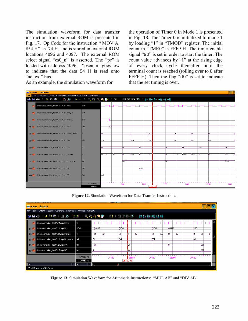
OP CODE : D8 DJNZ R0, ADDR
Go to State 1
pc = {pc[15:8],ad}
pc = pc + 1 temp = 0?
rom_addr = pc
3
290
NO
YES
292
291
OP Code: D8 DJNZ R0, ADDR
OP Code: 82 ANL C, BIT_ADDR 3
3 rom_addr = pc
temp1 = ad/8
temp2 = ad%8
temp1 = temp1 + 20 H
temp = ram [temp1]
225
226
227
bit1 = temp [temp2]
228
cy = cy & bit1
pc = pc + 1
229
Go to State 1
Figure 11 ASM
Chart for Bit
Manipulation
Instruction
Figure 11 ASM
Chart for Bit
Manipulation
Instruction
220
“DJNZ R0, code address” and bit manipulation
instruction “ANL C, bit address” are shown in
Fig. 10 and Fig. 11 respectively. These ASMs
can be analyzed in a similar manner to that
presented earlier. Byte and bit manipulation
instructions are realized in Immediate, Register,
Direct and Indirect Addressing Modes in the
present work. All the 8051 instructions have
been coded. Table 1 presents some of the
instructions realized along with their processing
times. Each instruction is presented in different
addressing modes. The execution speed of the
proposed Verilog realization of our system with
the existing classical 8051 system is also
compared. The proposed implementation scores
over the classical 8051 especially for
instructions such as “MUL AB” and “DIV
AB”. As can be seen from Table 1, the
proposed IP Core is faster than the existing
classical 8051 systems by over a range of 8 to
54 times.
5. SIMULATION RESULTS
The complete IP Core was coded in RTL
compliant Verilog. The simulation was run on
Modelsim and the results for various groups of
instructions such as data transfer, arithmetic,
logic, bit manipulation and external ROM
access are presented in this section. The
processing times of individual instructions are
presented in Table 1. It may be noted that the
waveforms are in conformity with the execution
of the instructions of the Intel‟s 8051
microcontroller. The Timer operations have
also been realized.
The simulation waveform for data transfer
instruction is presented in Fig. 12. As an
example, execution of “MOV A, #54 H” is
shown in the waveform. The Op code for this
instruction is 74 H. This instruction transfers 54
H data in to the “A” register as revealed in Fig.
12. The first signal from the top is the system
“clk” operating at 50 MHz frequency. Both the
“pc” and the “rom_address” are 0. The “state”
represents the current operating state of the
controller. The “ad” bus has 74 H on it to
indicate that the first fetch is the Op code. Next
fetch from the ROM is the data 54 H. On the
“ad” line, 54 H appears at the appropriate time.
The total number of cycles taken to complete
this instruction is 80 ns, i.e., 4 clock periods.
This timing is presented in Table 1.
Fig. 13 presents the Arithmetic operation
“MUL AB” and “DIV AB”. The Op code for
multiplication is A4 H and that of division is 84
H. For “MUL AB” operation, the “A” register
contents are FF H and that of B register is FF H
before the execution of the instruction. After
the execution, “A” register has 1, being the
lower byte of the product and, the upper byte
FE H is stored in register B. Similarly “DIV
AB” instruction divides A by B and the LSB
result manifests in A register while the
remainder appears in B. It takes 4 clock cycles
to execute each of these instructions and is
tabulated in Table 1.
The simulation waveform for “DA A
“instruction is shown in Fig. 14. After the
addition of two numbers 59 H and 54 H, “A”
register is adjusted for BCD result which is
equal to decimal number 13.
The simulation waveform for Logical
instruction is presented in Fig. 15. The
instruction “ORL A, #33 H” performs the
bitwise ORing of the accumulator content “DF
H” and the immediate data 33 H producing the
result “FF H. The operation takes 100 ns.
The simulation waveform for Bit manipulation
instruction such as “CPL C”, “CLR C” and
“SETB C” are presented in Fig. 16. These
instructions have Op codes B3 H, C3 H and D3
H respectively. The carry flag “CY” is initially
at logic level „0‟ and after the execution of the
instruction “CPL C” , “CY” flag goes high. For
“CLR C” instruction, CY flag is cleared.
Similarly, for the instruction “SETB C”, the
carry flag goes high. It takes 80 ns each to
execute these instructions and is tabulated in
Table 1.
221
The simulation waveform for data transfer
instruction from external ROM is presented in
Fig. 17. Op Code for the instruction “ MOV A,
#54 H” is 74 H and is stored in external ROM
locations 4096 and 4097. The external ROM
select signal “cs0_n” is asserted. The “pc” is
loaded with address 4096. “psen_n” goes low
to indicate that the data 54 H is read onto
“ad_ext” bus.
As an example, the simulation waveform for
the operation of Timer 0 in Mode 1 is presented
in Fig. 18. The Timer 0 is initialized to mode 1
by loading “1” in “TMOD” register. The initial
count in “TMR0” is FFF9 H. The timer enable
signal “tr0” is set in order to start the timer. The
count value advances by “1” at the rising edge
of every clock cycle thereafter until the
terminal count is reached (rolling over to 0 after
FFFF H). Then the flag “tf0” is set to indicate
that the set timing is over.
Figure 12. Simulation Waveform for Data Transfer Instructions
Figure 13. Simulation Waveform for Arithmetic Instructions: “MUL AB” and “DIV AB”
222
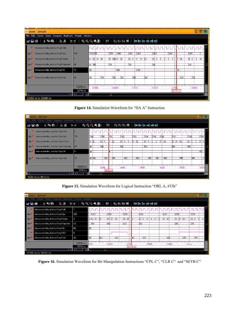
Figure 14. Simulation Waveform for “DA A” Instruction
Figure 15. Simulation Waveform for Logical Instruction “ORL A, #33h”
Figure 16. Simulation Waveform for Bit Manipulation Instructions “CPL C”, “CLR C“ and “SETB C”
223
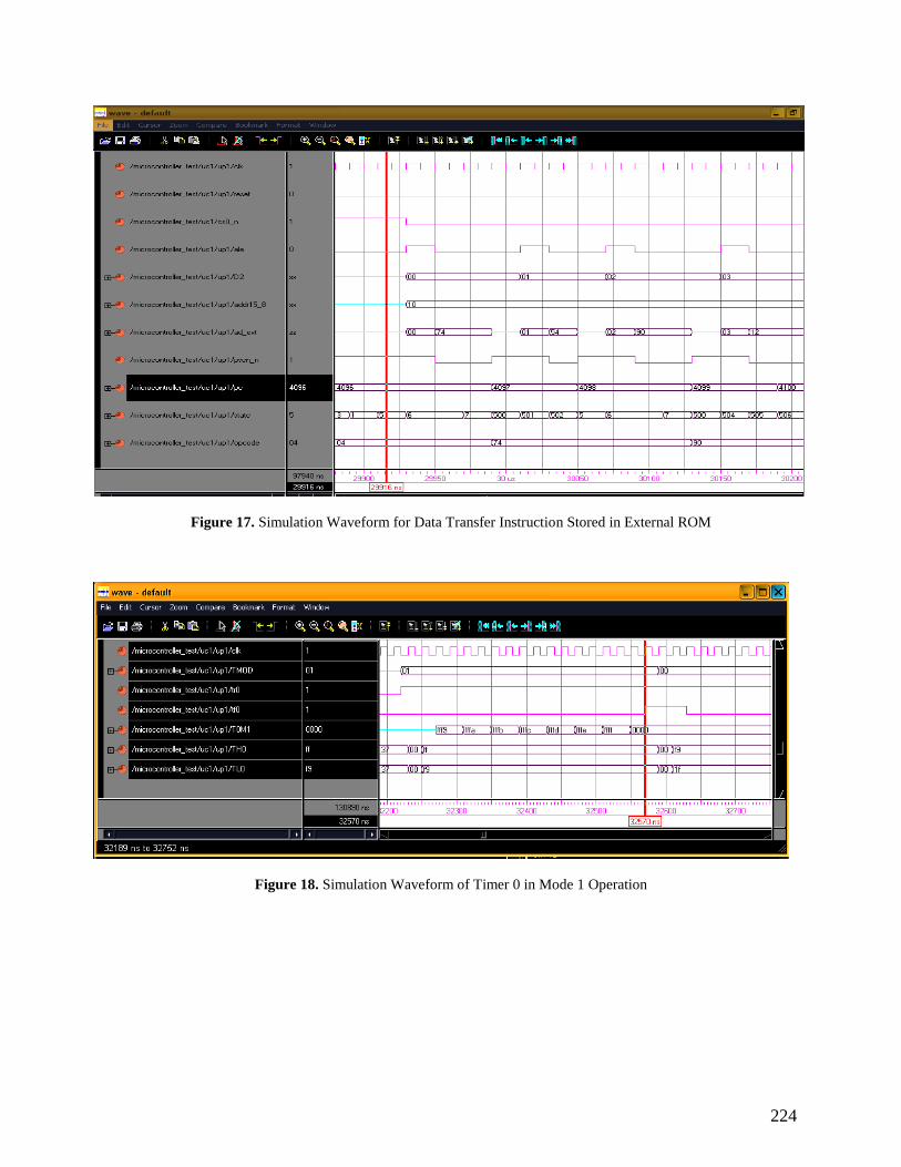
Figure 17. Simulation Waveform for Data Transfer Instruction Stored in External ROM
Figure 18. Simulation Waveform of Timer 0 in Mode 1 Operation
224
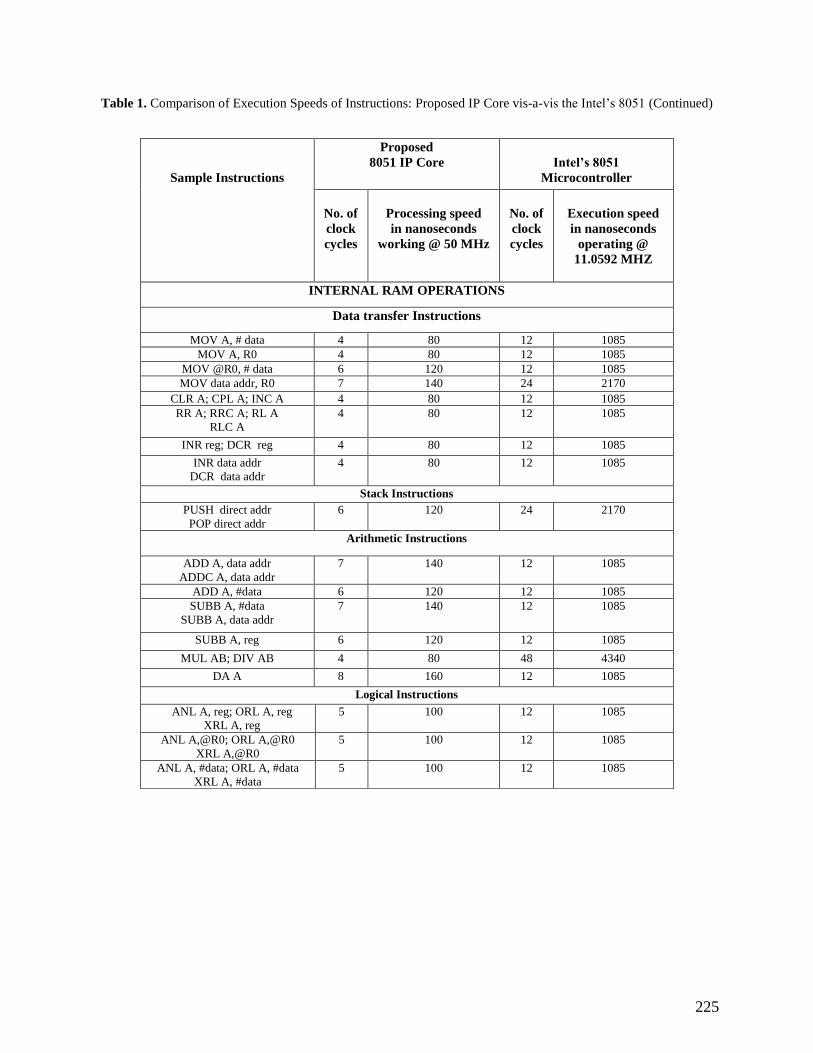
Table 1. Comparison of Execution Speeds of Instructions: Proposed IP Core vis-a-vis the Intel‟s 8051 (Continued)
Sample Instructions
Proposed
8051 IP Core
Intel’s 8051
Microcontroller
No. of
clock
cycles
Processing speed
in nanoseconds
working @ 50 MHz
No. of
clock
cycles
Execution speed
in nanoseconds
operating @
11.0592 MHZ
INTERNAL RAM OPERATIONS
Data transfer Instructions
MOV A, # data 4 80 12 1085
MOV A, R0 4 80 12 1085
MOV @R0, # data 6 120 12 1085
MOV data addr, R0 7 140 24 2170
CLR A; CPL A; INC A 4 80 12 1085
RR A; RRC A; RL A
RLC A
4 80 12 1085
INR reg; DCR reg 4 80 12 1085
INR data addr
DCR data addr
4 80 12 1085
Stack Instructions
PUSH direct addr
POP direct addr
6 120 24 2170
Arithmetic Instructions
ADD A, data addr
ADDC A, data addr
7 140 12 1085
ADD A, #data 6 120 12 1085
SUBB A, #data
SUBB A, data addr
7 140 12 1085
SUBB A, reg 6 120 12 1085
MUL AB; DIV AB 4 80 48 4340
DA A 8 160 12 1085
Logical Instructions
ANL A, reg; ORL A, reg
XRL A, reg
5 100 12 1085
ANL A,@R0; ORL A,@R0
XRL A,@R0
5 100 12 1085
ANL A, #data; ORL A, #data
XRL A, #data
5 100 12 1085
225
Table 1. Comparison of Execution Speeds of Instructions: Proposed IP Core vis-a-vis the Intel‟s 8051
Sample Instructions
Proposed FPGA
Implementation of our System
Existing Classical
8051 System
No. of
clock
cycles
Processing speed
in nanoseconds
working @ 50MHz
No. of
clock
cycles
Execution
speed
in
nanoseconds
operating @
11.0592MHZ
Logical Instructions
ANL direct addr, A
ORL direct addr, A
XRL direct addr, A
6 120 12 1085
ANL direct addr, # data
ORL direct addr, # data
XRL direct addr, # data
7 140 24 2170
Data Exchange Instructions
SWAP A 4 80 12 1085
XCH A, data addr 7 140 12 1085
XCH A,reg 6 120 12 1085
XCH A,@R0 6 120 12 1085
XCHD A,@R0 7 140 12 1085
BIT Manipulation Instructions
ORL C, bit addr
ANL C, bit addr
XRL C, bit addr
9 180 24 2170
MOV C, bit addr
MOV bit addr, C
9 180 24 2170
CPL bit addr
SETB bit addr
CLR bit addr
9 180 24 2170
CPL C; CLR C; SETB C 4 80 12 1085
JB bit addr, bit addr
JNB bit addr, bit addr
9 180 24 2170
Jump and Call Instructions
JZ code addr 4 80 24 2170
CJNE A, #data, rel addr 6 120 24 2170
LCALL 16 bit addr 13 260 24 2170
LJMP 16 bit addr 6 120 24 2170
JMP @A + DPTR 7 140 24 2170
SJMP code addr 5 100 24 2170
DJNZ reg, data addr 7 140 24 2170
EXTERNAL ROM OPERATIONS
Data Transfer Instructions
MOVX A, #data 8 160 24 2170
MOVX @DPTR, A 10 200 24 2170
MOVX A,@R0 11 220 24 2170
MOV DPTR, # 16 bit data 13 260 24 2170
226
6. CONCLUSIONS AND FUTURE WORK
IP Core has been designed for a
Microcontroller system for developing a Robot
based Agricultural Implement. The Verilog
design of the system conforms to RTL coding
guidelines and is independent of platform and
technology. The IP Core was designed with 4K
internal ROM and 128 bytes of internal RAM.
The external memory designed is of size 60 K
bytes for ROM and 64 K bytes for RAM. The
design includes the realization of two timers.
Test bench has also been developed using
Verilog to validate the instructions as well as
the resources designed. The designed IP Core is
faster than the Intel‟s 8051 microcontroller by 8
to 54 times depending upon the complexity of
REFERENCES
[1] Yuanyuan, Liu Jia and Liu Runsheng. : Single-Chip
Speech Recognition System Based on 8051
MicrocontroIler Core. In: Proc. IEEE Transactions on
Consumer Electronics, Vol. 47, pp. 149--153 (2001).
[2] A. Moore Scott.: 8080 compatible CPU in Verilog,
http://opencores.org/project,cpu8080.
[3] Aviral Mittal, Philips Semiconductors, Southampton,
UK. : http://www.vlsiip.com/vhdl/8085.vhd.
[4] R. V. Siva Reddy, S. Ramachandran and K.
Nagabhushana Raju.: IP Core Design for Electrostatic
Precipitator Controller System. In: Proc. 2010
International Conference on Advances in Information,
Communication Technology and VLSI Design
(ICAICV), PSG College of Technology, Coimbatore
(2010).
[5] S. Ramachandran. : Digital VLSI Systems Design,
Springer, Netherlands (2007).
[6] Noboru Noguchi, Michio Kise, Kazunobu Ishii and
Hideo Terao.: Field Automation using Robot Tractor. In:
Proc. Conference in Automation Technology for Off-
Road Equipment, pp. 239--245. The American Society of
Agricultural and Biological Engineers, St. Joseph,
Michigan (2002).
[7] K. C. Jones.: Tools Carrying Robots Could Weed
Out Tedious Farming Tasks. In: Information Week, July
5 (2007).
the instructions realized. The system runs using
a conservative operational frequency of 50
MHz to suit Spartan 3, 200 FPGA. The same
Core can also work on faster FPGAs at 100
MHz or more and ASICs at 400 MHz or more
since the design is truly platform and
technology independent. The IP core developed
can be used for all applications, whether they
are for a past product, the current ongoing
project or for future applications. It may be
noted that 8051 microcontroller is given a new
lease of life by the present work. Presently, the
serial communication and the Robot based
Agricultural Implement core are being
developed.
[8] D. W. I. Brooke.: Automata for Agriculture-
Driverless Tractor System, Kybernetes, Vol. 4, Iss: 1, pp.
29--32. MCB UP Ltd (1975).
[9] Zhang, X., Geimer, M., Grandl, L., and
Kammerbauer, B.: Vehicular Electronics and Safety. In:
Proc. IEEE International Conference on Vehicular
Electronics and Safety (ICVES), pp. 156--161 (2009).
[10] Chen Jun et al.: On-Tracking Control of Agricultural
Mobile Robot Based on Inner Information. In: Proc.
2011 Computer Distributed Control and Intelligent
Environmental Monitoring (CDCIEM), pp. 103--106,
(2011).
[11] Eaton, R., Katupitiya, J., Siew. K,W. and
Howarth, B. : Autonomous Farming: Modeling and
Control of Agricultural Machinery in a Unified
Framework. pp. 499-504, Mechatronics and Machine
Vision in Practice (M2VIP) (2008).
[12] Muhammad Ali Mazidi and Janice Gillispie Mazidi:
The 8051 Microcontroller and Embedded Systems,
Pearson Education (2002).
[13] Kenneth J. Ayala.: The 8051 Microcontroller
Architecture, Programming and Applications, Penram
International India (1997).
[14] Raj Kamal.: Microcontollers Architecture,
Programming, Interfacing and System Design, Pearson
Education (2008).
227